

Page 1
Integrated Device Technology, Inc.
24-BIT BUS EXCHANGE
SWITCH
IDT74FST163213
PRODUCT PREVIEW
FEATURES:
• Bus switches provide zero delay paths
• Extended commercial range of –40°C to +85°C
• Low switch on-resistance:
FST163xxx – 4Ω
• TTL-compatible input and output levels
• ESD > 2000V per MIL-STD-883, Method 3015;
> 200V using machine model (C = 200pF, R = 0)
• Available in SSOP, TSSOP and TVSOP
DESCRIPTION:
The FST163213 belongs to IDT's family of Bus switches.
Bus switch devices perform the function of connecting or
isolating two ports without providing any inherent current sink
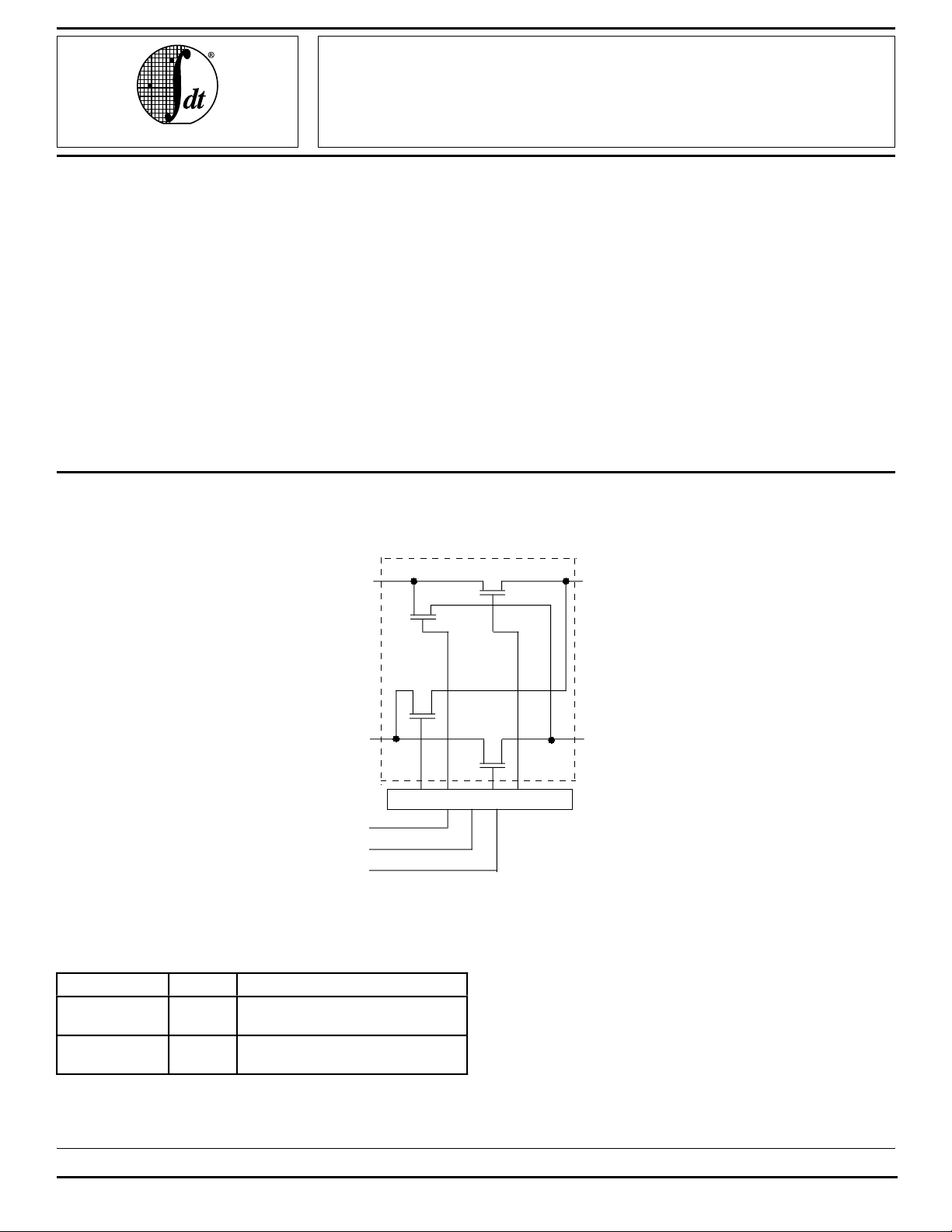
FUNCTIONAL BLOCK DIAGRAM
1 of 12 Channels
1A1
or source capability. Thus they generate little or no noise of
their own while providing a low resistance path for an external
driver. These devices connect input and output ports through
an n-channel FET. When ther gate-to-source junction of this
FET is adequately forward-biased the device conducts and
the resistance between input and output ports is small. Without adequate bias on the gate-to-source junction of the FET,
the FET is turned off, therefore with no VCC applied, the device
has hot insertion capability.
The low on-resistance and simplicity of the connection
between input and output ports reduces the delay in this path
to close to zero.
The FST163213 provides four 12-bit TTL-compatible ports
that support 2 way bus exchange. The S0-2 pins control the
bus exchange and switch enable functions.
B
1
1
1
A
2
Flow Control
S
0
S
1
S
2
1B2
3684 drw 01
PIN DESCRIPTION
Pin Names I/O Description
A1, A2
B1, B2
S0-2 I Control Pins for Mux and Switch
The IDT logo is a registered trademark of Integrated Device Technology, Inc.
COMMERCIAL TEMPERATURE RANGE FEBRUARY 1997
1997 Integrated Device Technology, Inc. DSC-3684/-
I/O Buses A1, A2, B1, B2
Enable Functions
3684 tbl 01
1
Page 2
IDT74FST163213
24-BIT BUS EXCHANGE SWITCH COMMERCIAL TEMPERATURE RANGE
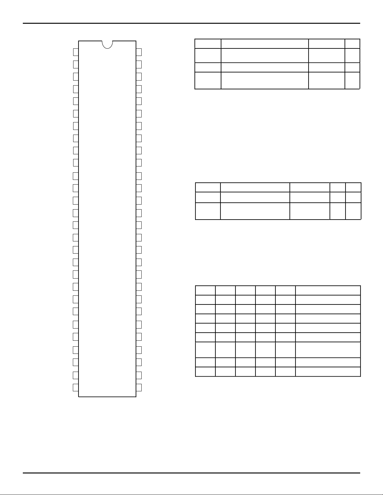
PIN CONFIGURATION
S0
1
A1
A2
A1
A2
A1
A2
A1
A2
A1
A2
2
3
4
5
6
7
8
9
10
11
12
13
14
15
16
1
1
2
2
3
3
GND
4A1
4A2
5A1
5A2
6
6
7
7
SO56-1
SO56-2
SO56-3
56
55
54
53
52
51
50
49
48
47
46
45
44
43
42
41
S1
S2
1
B1
1
B2
2
B1
2
B2
3
B1
GND
B2
3
B1
4
4
B2
B1
5
5
B2
B1
6
6
B2
7
B1
ABSOLUTE MAXIMUM RATINGS
(1)
Symbol Description Max. Unit
(2)
VTERM
Terminal Voltage with Respect
–0.5 to +7.0 V
to GND
TSTG Storage Temperature –65 to +150 °C
IOUT Maximum Continuous Channel
128 mA
Current
(2)
Typ. Unit
3684 lnk 02
NOTES:
1. Stresses greater than those listed under ABSOLUTE MAXIMUM RATINGS may cause permanent damage to the device. This is a stress rating
only and functional operation of the device at these or any other conditions above those indicated in the operational sections of this specification is not implied. Exposure to absolute maximum rating condiitions for
extended periods may affect reliability.
2. VCC, Control and Switch terminals.
CAPACITANCE
(1)
Symbol Parameter Conditions
CIN Control Input Capacitance 4 pF
CI/O
Switch Input/Output
Switch Off
pF
Capacitance
NOTES:
1. Capacitance is characterized but not tested
2. TA = 25°C, f = 1MHz, VIN = 0V, VOUT = 0V
3684 lnk 03
VCC
A1
8
GND
17
18
19
40
39
38
B2
7
B1
8
GND
FUNCTION TABLE
8A2
9
9A2
10A1
10A2
11
11A2
12A1
12A2
20
21
A1
22
23
24
25
A111B1
26
27
28
SSOP/
TSSOP/TVSOP
TOP VIEW
37
36
35
34
33
32
31
30
29
8B2
9
B1
B2
9
10
10
11
12
12
B1
B2
B2
B1
B2
3684 drw 02
S
2
L L L Z Z Disconnect
LLHB
LHLB
LHHZB
HLLZB
HLHA
HHLB
HHHB
S
1
S
0
A
1
A
1
2
2
&
B
2
1
2
2
ZA
ZA
1
2
ZA
B
2
B
1
Function
1
to B
1
1
to B
2
A
2
to B
1
A
2
to B
2
1
to A2 and B
A1 to B1, A2 to B
A1 to B2, A2 to B
2
2
1
3684 tbl 04
2
Page 3
DT74FST163213
24-BIT BUS EXCHANGE SWITCH COMMERCIAL TEMPERATURE RANGE
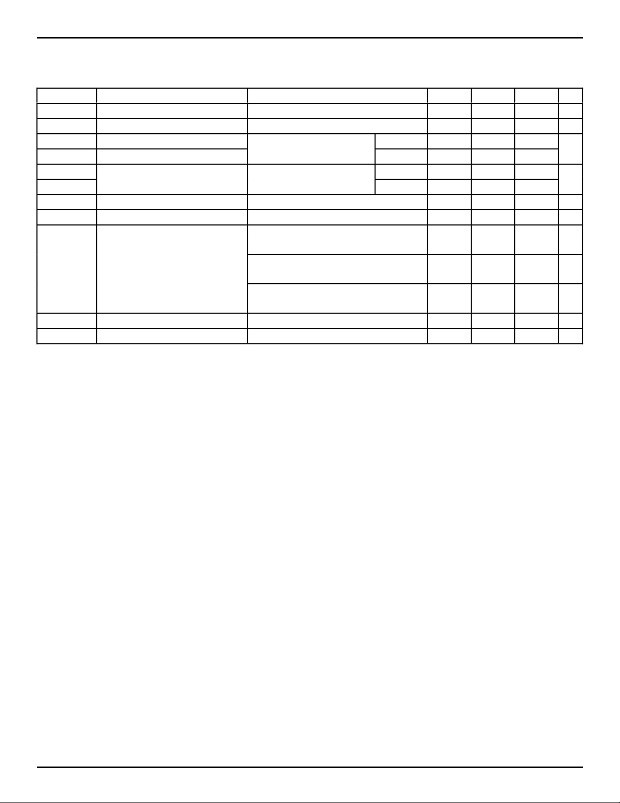
DC ELECTRICAL CHARACTERISTICS OVER OPERATING RANGE
Following Conditions Apply Unless Otherwise Specified:
Commercial: TA = –40°C to +85°C, VCC = 5.0V ±10%
Symbol Parameter Test Conditions
(1)
Min. Typ.
VIH Input HIGH Voltage Guaranteed Logic HIGH for Control Inputs 2.0 — — V
VIL Input LOW Voltage Guaranteed Logic LOW for Control Inputs — — 0.8 V
II H Input HIGH Current VCC = Max. VI = VCC ——±1µA
II L Input LOW Voltage VI = GND — — ±1
IOZH High Impedance Output Current VCC = Max. VO = VCC ——±1µA
IOZL (3-State Output pins) VO = GND — — ±1
IOS Short Circuit Current VCC = Max., VO = GND
(3)
— 300 — mA
VIK Clamp Diode Voltage VCC = Min., IIN = –18mA — –0.7 –1.2 V
RON Switch On Resistance
(4)
VCC = Min. VIN = 0.0V — 4 7 Ω
ION = 64mA
VCC = Min. VIN = 0.0V — 4 7 Ω
ION = 30mA
VCC = Min. VIN = 2.4V — 10 15 Ω
ION = 15mA
IOFF Input/Output Power Off Leakage VCC = 0V, VIN or VO ≤ 4.5V — — ±1 µA
ICC Quiescent Power Supply Current VCC = Max., VIN = GND or VCC — 0.1 3 µA
NOTES:
1. For conditions shown as Max. or Min. use appropriate value specified under Electrical Characteristics for the applicable device type.
2. Typical values are at VCC = 5.0V, +25°C ambient.
3. Not more than one output should be testes at one time. Duration of the test should not exceed one second.
4. Measured by voltage drop between ports at indicated current through the switch.
(2)
Max. Unit
3684 tbl 05
3
Page 4
IDT74FST163213
24-BIT BUS EXCHANGE SWITCH COMMERCIAL TEMPERATURE RANGE
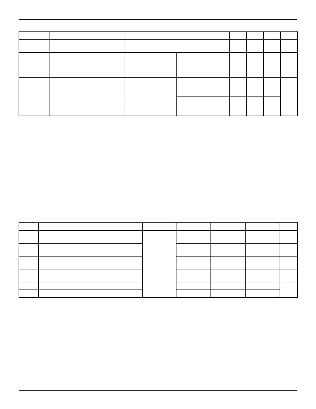
POWER SUPPLY CHARACTERISTICS
Symbol Parameter Test Conditions
∆ICC Quiescent Power Supply Current
TTL Inputs HIGH
ICCD Dynamic Power Supply
(4)
Current
VCC = Max.
V
IN = 3.4V
(3)
VCC = Max.
Outputs Open
(1)
VIN = VCC
VIN = GND
Min. Typ.
— 0.5 1.5 mA
—3040µA/
Enable Pin Toggling
50% Duty Cycle
IC Total Power Supply Current
(6)
VCC = Max.
Outputs Open
VIN = VCC
VIN = GND
— 7.2 9.6 mA
Enable Pins Toggling
(24 Switches Toggling)
fi = 10MHz
VIN = 3.4
V
IN = GND
— 7.7 11.1
50% Duty Cycle
NOTES:
1. For conditions shown as Max. or Min., use appropriate value specified under Electrical Characteristics for the applicable device type.
2. Typical values are at VCC = 5.0V, +25°C ambient.
3. Per TTL driven input (VIN = 3.4V). All other inputs at VCC or GND.
4. This parameter is not directly testable, but is derived for use in Total Power Supply Calculations.
5. Values for these conditions are examples of the ICC formula. These limits are guaranteed but not tested.
6. IC = IQUIESCENT + IINPUTS + IDYNAMIC
IC = ICC + ∆ICC DHNT + ICCD (fiN)
ICC = Quiescent Current
∆ICC = Power Supply Current for a TTL High Input (VIN = 3.4V)
DH = Duty Cycle for TTL Inputs High
NT = Number of TTL Inputs at DH
ICCD = Dynamic Current Caused by an Input Transition Pair (HLH or LHL)
fi = Input Frequency
N = Number of Switches Toggling at fi
All currents are in milliamps and all frequencies are in megahertz.
(2)
Max. Unit
MHz/
Switch
3684 tbl 06
SWITCHING CHARACTERISTICS OVER OPERATING RANGE
Following Conditions Apply Unless Otherwise Specified:
Commercial: TA = –40°C to +85°C, VCC = 5.0V ±10%
Symbol Description Condition
tPLH
tPHL
Data Propagation Delay
A to B, B to A
(3,4)
CL = 50pF
R
L = 500Ω
(1)
tBX Switch Multiplex Delay
S to A, B
tPZH
tPZL
tPHZ
tPLZ
|QCI| Charge Injection, Typical
|QDCI| Charge Injection, Typical
NOTES:
1. See test circuit and waveforms.
2. Minimum limits guaranteed but not tested.
3. This parameter is guaranteed by design but not tested.
4. The bus switch contributes no propagation delay other than the RC delay of the on resistance of the switch and the load capacitance. The time constant
for the switch alone is of the order of 2.5ns for 50pF load. Since this time is constant and much smaller than the rise/fall times of typical driving signals,
it adds very little propagation delay to the system. Propagation delay on the bus switch when used in a system is determined by the driving circuit on the
driving side of the switch and its interaction with the load on the driven side.
5. Measured at switch turn off, load = 50 pF in parallel with 10 MΩ scope probe, VIN = 0.0 volts.
6. Measured at switch turn off through bus multiplexer, (e.g.- A1 to B1 = >A1 to B2), load = 50 pF in parallel with 10 MΩ scope probe, VIN at A = 0.0 volts.
Charge injection is reduced because the injection from the turn off of the A1 to B1 switch is compensated by the turn on of the A1 to B2 switch.
7. Characterized parameter. Not 100% tested.
Switch Turn on Delay
S to A, B
Switch Turn off Delay
S to A, B
(3)
(5,7)
(6,7)
(2)
Min.
Typ. Max. Unit
— — 0.25 ns
1.5 — 6.5 ns
1.5 — 6.5 ns
1.5 — 7 ns
— 1.5 — pC
— 0.5 —
3684 tbl 07
4
Page 5
DT74FST163213
24-BIT BUS EXCHANGE SWITCH COMMERCIAL TEMPERATURE RANGE
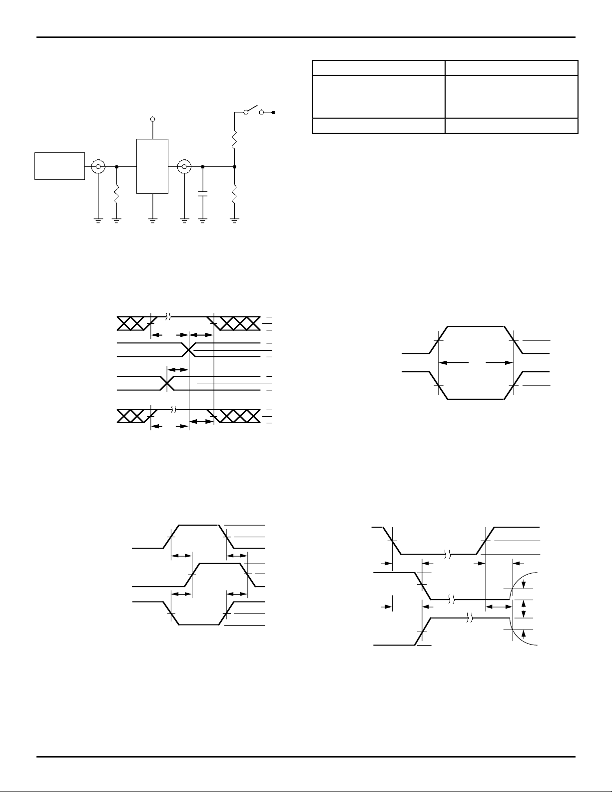
TEST CIRCUITS AND WAVEFORMS
TEST CIRCUITS FOR ALL OUTPUTS
V
CC
V
OUT
Pulse
Generator
V
IN
D.U.T.
50pF
T
R
C L
SET-UP, HOLD AND RELEASE TIMES
DATA
INPUT
TIMING
INPUT
ASYNCHRONOUS CONTROL
PRESET
CLEAR
ETC.
SYNCHRONOUS CONTROL
PRESET
CLEAR
CLOCK ENABLE
ETC.
tSU
tSU
tH
tREM
tH
500Ω
500Ω
7.0V
3684 drw 03
3V
1.5V
0V
3V
1.5V
0V
3V
1.5V
0V
3V
1.5V
0V
3684 drw 04
SWITCH POSITION
Test Switch
Open Drain
Disable Low
Closed
Enable Low
All Other Tests
DEFINITIONS:
CL= Load capacitance: includes jig and probe capacitance.
RT = Termination resistance: should be equal to ZOUT of the Pulse
Generator.
Open
PULSE WIDTH
LOW-HIGH-LOW
HIGH-LOW-HIGH
PULSE
tW
PULSE
3684 lnk 08
1.5V
1.5V
3684 drw 05
PROPAGATION DELAY
SAME PHASE
INPUT TRANSITION
tPLH
OUTPUT
tPLH tPHL
OPPOSITE PHASE
INPUT TRANSITION
tPHL
3V
1.5V
0V
V
OH
1.5V
VOL
3V
1.5V
0V
3684 drw 06
ENABLE AND DISABLE TIMES
ENABLE DISABLE
3V
CONTROL
INPUT
t
PLZtPZL
OUTPUT
NORMALLY
LOW
SWITCH
CLOSED
3.5V
1.5V
tPZH tPHZ
OUTPUT
NORMALLY
HIGH
NOTES:
1. Diagram shown for input Control Enable-LOW and input Control DisableHIGH
2. Pulse Generator for All Pulses: Rate ≤ 1.0MHz; tF ≤ 2.5ns; tR ≤ 2.5ns
5
SWITCH
OPEN
1.5V
0V
0.3V
0.3V
1.5V
0V
3.5V
VOL
VOH
0V
3684 drw 07
Page 6
IDT74FST163213
24-BIT BUS EXCHANGE SWITCH COMMERCIAL TEMPERATURE RANGE
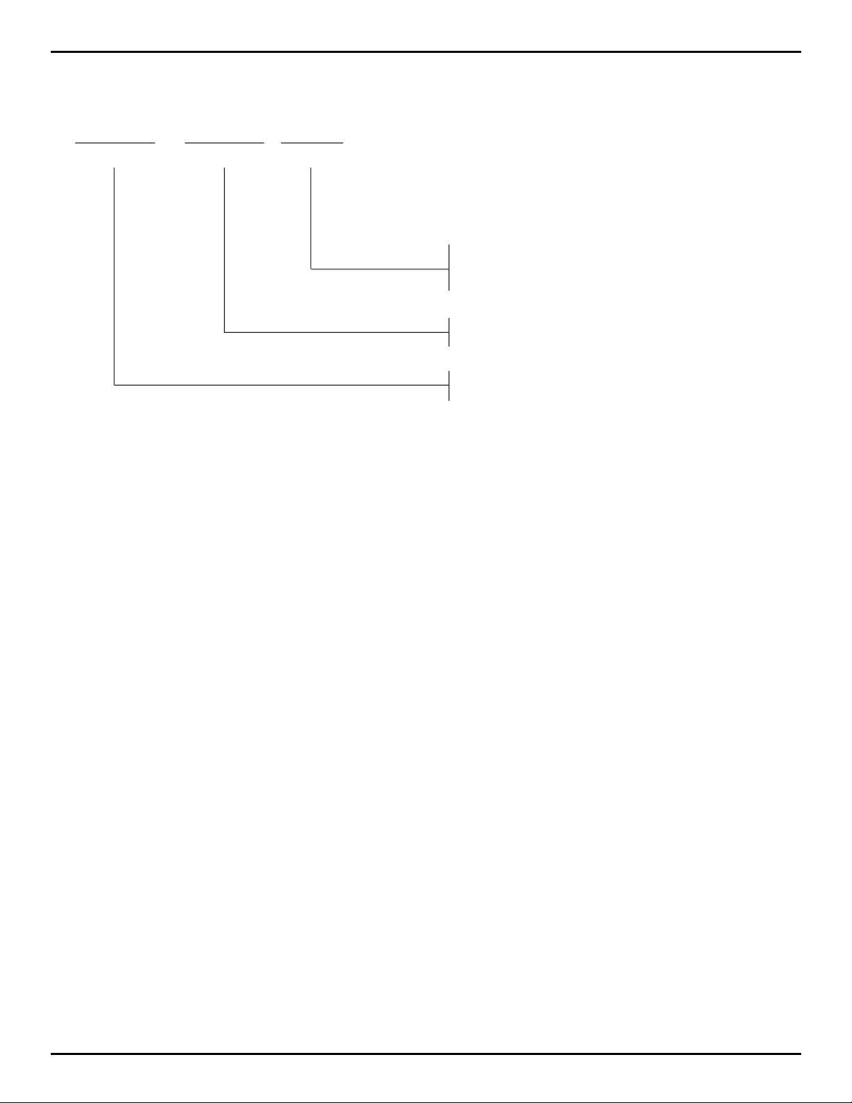
ORDERING INFORMATION
IDT XX
Temp. Range
FST
Device Type
16 XX
X
Package
PV
PA
PF
163213
Shrink Small Outline Package (SO56-1)
Thin Shrink Small Outline Package (SO56-2)
Thin Very Small Outline Package (SO56-3)
24-Bit Bus Exchange Switch
74 –40°C to +85°C
3684 drw 08
6
Page 7

WWW.ALLDATASHEET.COM
Copyright © Each Manufacturing Company.
All Datasheets cannot be modified without permission.
This datasheet has been download from :
www.AllDataSheet.com
100% Free DataSheet Search Site.
Free Download.
No Register.
Fast Search System.
www.AllDataSheet.com
 Loading...