

Datasheet IDT72205LB25TFB, IDT72205LB35G, IDT72205LB35GB, IDT72205LB35J, IDT72205LB35JB Datasheet (Integrated Device Technology Inc)
...Page 1
Integrated Device Technology, Inc.
CMOS SyncFIFO
256 x 18, 512 x 18, 1024 x 18, 2048 x
18 and 4096 x 18
IDT72205LB
IDT72215LB
IDT72225LB
IDT72235LB
IDT72245LB
FEATURES:
• 256 x 18-bit organization array (72205LB)
• 512 x 18-bit organization array (72215LB)
• 1024 x 18-bit organization array (72225LB)
• 2048 x 18-bit organization array (72235LB)
• 4096 x 18-bit organization array (72245LB)
• 15 ns read/write cycle time
• Easily expandable in depth and width
• Read and write clocks can be asynchronous or coincident
• Dual-Port zero fall-through time architecture
• Programmable almost-empty and almost-full flags
• Empty and Full flags signal FIFO status
• Half-Full flag capability in a single device configuration
• Output enable puts output data bus in high-impedance
state
• High-performance submicron CMOS technology
• Available in a 64-lead thin quad flatpack (TQFP/STQFP),
pin grid array (PGA), and plastic leaded chip carrier
(PLCC)
• Military product compliant to MIL-STD-883, Class B
• Industrial temperature range (-40
O
C to +85OC) is avail-
able, tested to military electrical specifications
DESCRIPTION:
The IDT72205LB/72215LB/72225LB/72235LB/72245LB
are very high-speed, low-power First-In, First-Out (FIFO)
memories with clocked read and write controls. These FIFOs
are applicable for a wide variety of data buffering needs, such
as optical disk controllers, Local Area Networks (LANs), and
interprocessor communication.
Both FIFOs have 18-bit input and output ports. The input
port is controlled by a free-running clock (WCLK), and a data
input enable pin (
FIFO on every clock when
WEN
). Data is read into the synchronous
WEN
is asserted. The output port
is controlled by another clock pin (RCLK) and another enable
pin (
REN
). The read clock can be tied to the write clock for
single clock operation or the two clocks can run asynchronous
of one another for dual-clock operation. An Output Enable pin
(OE) is provided on the read port for three-state control of the
output.
The synchronous FIFOs have two fixed flags, Empty (EF)
and Full (FF), and two programmable flags, Almost-Empty
(
PAE
) and Almost-Full (
PAF
). The offset loading of the programmable flags is controlled by a simple state machine, and
is initiated by asserting the Load pin (LD). A Half-Full flag (HF)
is available when the FIFO is used in a single device configuration.
The IDT72205LB/72215LB/72225LB/72235LB/72245LB
are depth expandable using a daisy-chain technique. The XI
and XO pins are used to expand the FIFOs. In depth expansion configuration, FL is grounded on the first device and set
to HIGH for all other devices in the daisy chain.
The IDT72205LB/72215LB/72225LB/72235LB/72245LB is
fabricated using IDT’s high-speed submicron CMOS technology. Military grade product is manufactured in compliance
with the latest revision of MIL-STD-883, Class B.
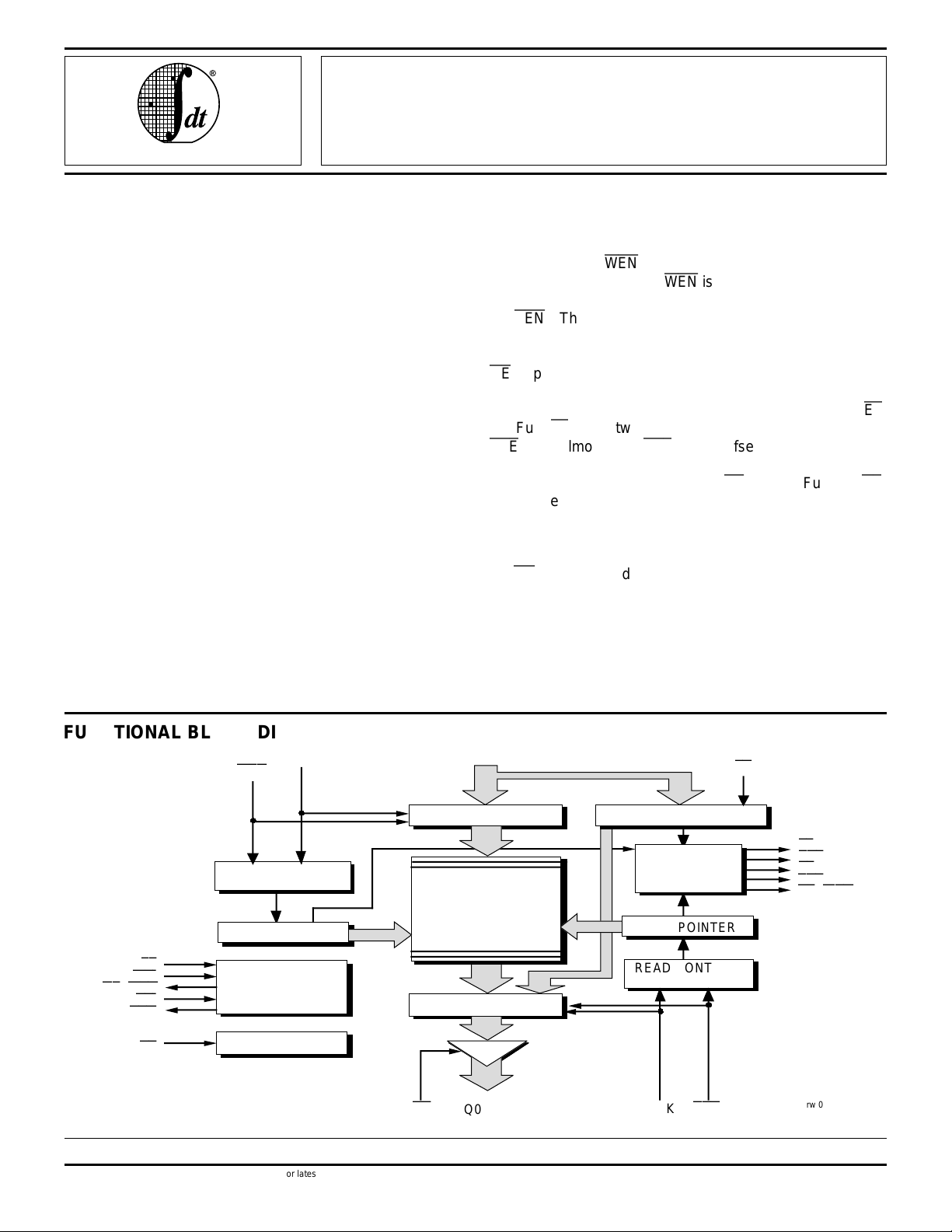
FUNCTIONAL BLOCK DIAGRAM
WEN
WRITE CONTROL
WRITE POINTER
FL
WXI
(HF)/
WXO
RXI
RXO
RS
SyncFIFO is a trademark and the IDT logo is a registered trademark of Integrated Device Technology, Inc
EXPANSION LOGIC
RESET LOGIC
WCLK D0-D17
INPUT REGISTER
LOGIC
256 x 18, 512 x 18
1024 x 18, 2048 x 18
OUTPUT REGISTER
OE
•
•
RAM ARRAY
4096 x 18
•
•
Q0-Q17
OFFSET REGISTER
FLAG
LOGIC
READ POINTER
READ CONTROL
LOGIC
RCLK
MILITARY AND COMMERCIAL TEMPERATURE RANGES DECEMBER 1996
1996 Integrated Device Technology, Inc. DSC-2766/7
For latest information contact IDT's web site at www.idt.com or fax-on-demand at 408-492-8391.
5.16 1
REN
LD
FF
PAF
EF
PAE
HF/(WXO
2766 drw 01
)
Page 2

IDT72205LB/72215LB/72225LB/72235LB/72245LB CMOS SyncFIFO
256 x 18, 512 x 18, 1024 x 18, 2048 x 18 and 4096 x 18 MILITARY AND COMMERCIAL TEMPERATURE RANGES
PIN CONFIGURATIONS
WXO
11
VCC
Q
3
GND
Q
0
HF
/
VCC
WEN
FLRXI
FF WXI
G68-1
RSEFLD
OE
PAF
RCLK
REN
Q1Q2
10
09
08
07
06
05
04
03
02
Q4
GND
Q6 Q5
Q7
VCC
GND
Q10 Q9
VCC
Q11
Q12
GND
Q14 Q13
V
CC
Q8
Q16Q15
01 GND GND
RXO
Pin 1 Designator
GND
VCC
VCCQ17
PAE
WCLK
GND
VCC
D17 D14
D16
D2
D6
D10
D12
D15
ABCDEFGHJKL
PGA
TOP VIEW
D0
D1
D3D4
D5
D7
D8
D9
D11
D13
2766 drw 02
D14
D13
D12
D11
D10
D9
VCC
D8
GND
D
D6
D5
D4
D3
D2
D1
D0
D16
GND
D17
RCLK
D15
98765432
10
RENLDOE
RS
GND
EF
VCC
6867666564636261
1
11
12
13
14
15
16
17
18
7
19
J68-1
20
21
22
23
24
25
26
27 28 29 30 31 32 33 34 35 36 37 38 39404142 43
PAE
FL
WEN
WCLK
WXI
CC
V
PAF
RXI
FF
HF
/
RXO
0
Q
WXO
CC
V
Q1
Q17
Q16
2
Q
GND
15
GND
Q
60
59
58
57
56
55
54
53
52
51
50
49
48
47
46
45
44
Q3
VCC
VCC
Q14
Q13
GND
Q
12
Q11
VCC
Q10
Q9
GND
8
Q
Q7
VCC
Q6
Q5
GND
Q
4
2766 drw 03
PLCC
TOP VIEW
5.16 2
Page 3
IDT72205LB/72215LB/72225LB/72235LB/72245LB CMOS SyncFIFO
256 x 18-BIT, 512 x 18, 1024 x 18, 2048 x 18 and 4096 x 18 MILITARY AND COMMERCIAL TEMPERATURE RANGES
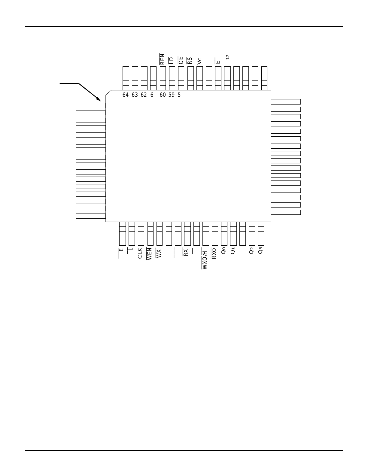
PIN CONFIGURATIONS
PIN 1
15
D
D14
D13
D12
D11
D10
D9
D8
D7
D6
D5
D4
D3
D2
D1
D0
16
D
17
D
GND
REN
RCLK
LDOERS
VCCGND
EF
17Q16
Q
64 63 62 61 60 59 58 57 56 55 54 53 52 51 50 49
1
2
3
4
5
6
7
8
PN 64-1
PP64-1
9
10
11
12
13
14
15
16
17 18 19 20 21 22 23 24 25 26 27 28 29 30 31 32
GND
15
Q
48
47
46
45
44
43
42
41
40
39
38
37
36
35
34
33
CC
V
Q14
Q13
GND
12
Q
Q11
VCC
Q10
Q9
GND
Q
8
Q7
Q6
Q5
GND
4
Q
VCC
FL
PAE
NOTE:
1. For information on the flatpack (F68-1), contact factory.
WEN
WCLK
CC
V
WXI
TQFP/STQFP
TOP VIEW
PAF
RXI
FF
HF
/
WXO
RXO
0Q1
Q
GND
3
2
Q
Q
2766 drw 04
5.16 3
Page 4
IDT72205LB/72215LB/72225LB/72235LB/72245LB CMOS SyncFIFO
256 x 18, 512 x 18, 1024 x 18, 2048 x 18 and 4096 x 18 MILITARY AND COMMERCIAL TEMPERATURE RANGES
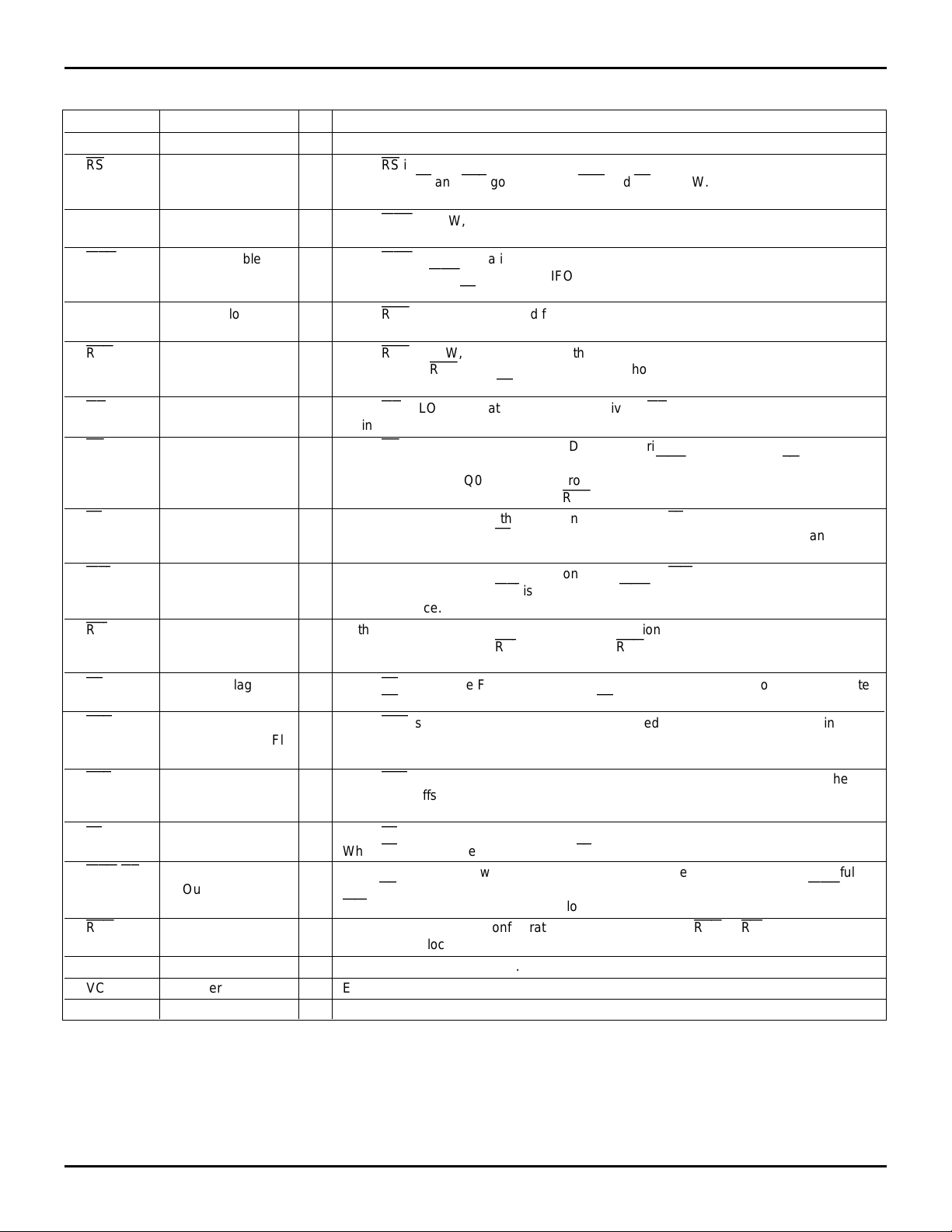
PIN DESCRIPTION
Symbol Name I/O Description
D0–D17 Data Inputs I Data inputs for a 18-bit bus.
RS
WCLK Write Clock I When
WEN
RCLK Read Clock I When
REN
OE
LD
FL
WXI
RXI
EF
PAE
PAF
FF
WXO/HF
RXO
Q0–Q17 Data Outputs O Data outputs for a 18-bit bus.
VCC Power Eight +5V power supply pins for the PLCC and PGA, five pins for the TQFP.
GND Ground Eight ground pins for the PLCC and PGA, seven pins for the TQFP.
Reset I When RS is set LOW, internal read and write pointers are set to the first location of the
RAM array, FF and
PAF
go HIGH, and
PAE
and EF go LOW. A reset is required before an
initial WRITE after power-up.
WEN
is LOW, data is written into the FIFO on a LOW-to-HIGH transition of WCLK,
if the FIFO is not full.
Write Enable I When
WEN
is LOW, data is written into the FIFO on every LOW-to-HIGH transition of
WCLK. When
WEN
is HIGH, the FIFO holds the previous data. Data will not be written
into the FIFO if the FF is LOW.
REN
is LOW, data is read from the FIFO on a LOW-to-HIGH transition of RCLK, if
the FIFO is not empty.
Read Enable I When
REN
is LOW, data is read from the FIFO on every LOW-to-HIGH transition of
RCLK. When
REN
is HIGH, the output register holds the previous data. Data will not be
read from the FIFO if the EF is LOW.
Output Enable I When OE is LOW, the data output bus is active. If OE is HIGH, the output data bus will
be in a high-impedance state.
Load I When LD is LOW, data on the inputs D0–D11 is written to the offset and depth registers
on the LOW-to-HIGH transition of the WCLK, when
WEN
is LOW. When LD is LOW,
data on the outputs Q0–Q11 is read from the offset and depth registers on the LOW-toHIGH transition of the RCLK, when
REN
is LOW.
First Load I In the single device or width expansion configuration, FL is grounded. In the depth
expansion configuration, FL is grounded on the first device (first load device) and set to
HIGH for all other devices in the daisy chain.
Write Expansion I In the single device or width expansion configuration,
Input expansion configuration,
WXI
is connected to
WXO
WXI
is grounded. In the depth
(Write Expansion Out) of the
previous device.
Read Expansion I In the single device or width expansion configuration, RXI is grounded. In the depth
Input expansion configuration,
RXI
is connected to
RXO
(Read Expansion Out) of the previous
device.
Empty Flag O When EF is LOW, the FIFO is empty and further data reads from the output are inhibited.
When EF is HIGH, the FIFO is not empty. EF is synchronized to RCLK.
Programmable O When
PAE
is LOW, the FIFO is almost empty based on the offset programmed into the
Almost-Empty Flag FIFO. The default offset at reset is 31 from empty for 72205LB, 63 from empty for
72215LB, and 127 from empty for 72225LB/72235LB/72245LB.
Programmable O When
PAF
is LOW, the FIFO is almost full based on the offset programmed into the FIFO.
The default offset at reset is 31 from full for 72205LB, 63 from full for 72215LB, and
127 from full for 72225LB/72235LB/72245LB.
Full Flag O When FF is LOW, the FIFO is full and further data writes into the input are inhibited.
When FF is HIGH, the FIFO is not full. FF is synchronized to WCLK.
Write Expansion O In the single device or width expansion configuration, the device is more than half full
Out/Half-Full Flag when HF is LOW. In the depth expansion configuration, a pulse is sent from
WXI
of the next device when the last location in the FIFO is written.
Read Expansion O In the depth expansion configuration, a pulse is sent from
RXO
to
RXI
WXO
to
of the next device
Out when the last location in the FIFO is read.
2766 tbl 01
5.16 4
Page 5
IDT72205LB/72215LB/72225LB/72235LB/72245LB CMOS SyncFIFO
256 x 18-BIT, 512 x 18, 1024 x 18, 2048 x 18 and 4096 x 18 MILITARY AND COMMERCIAL TEMPERATURE RANGES
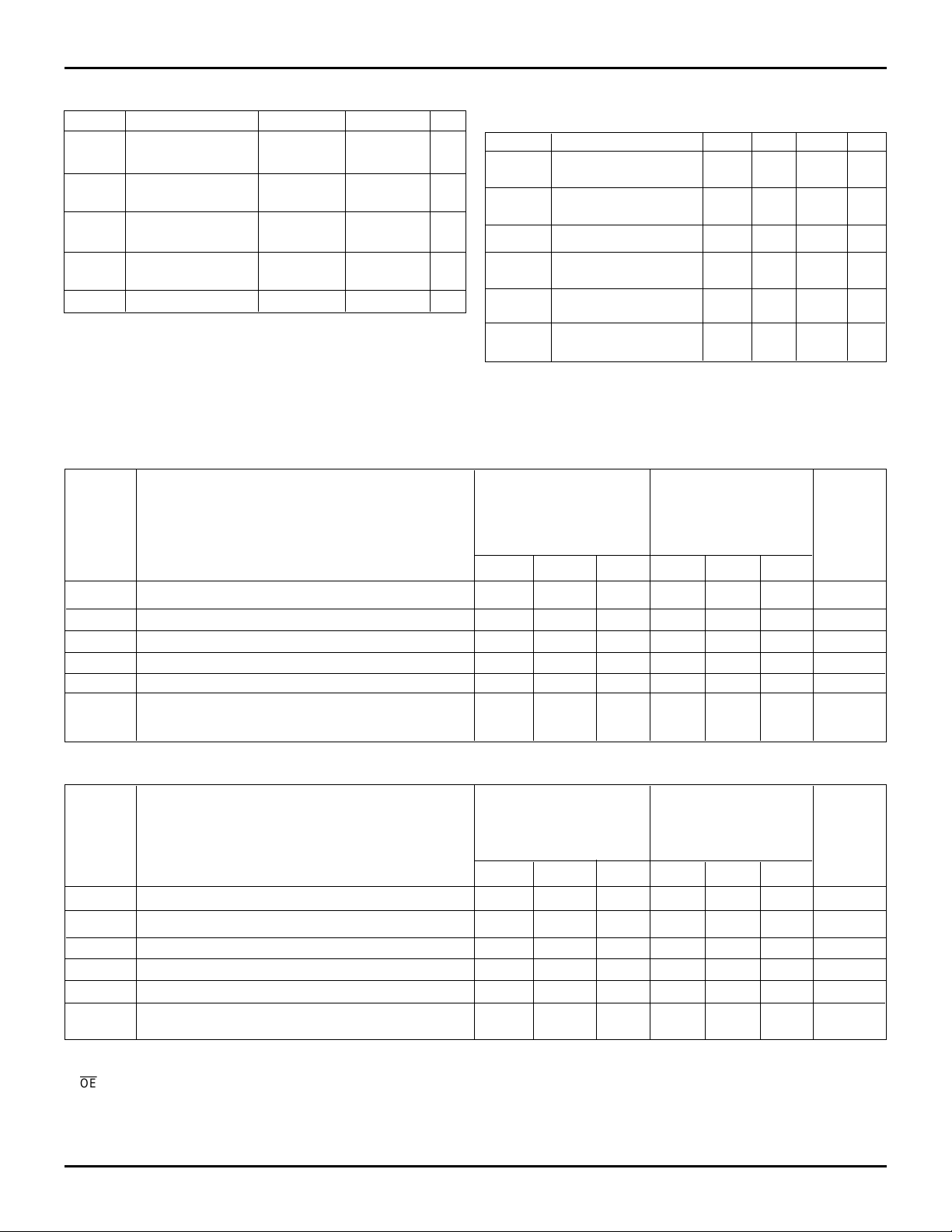
ABSOLUTE MAXIMUM RATINGS
Symbol Rating Commercial MIilitary Unit
V
TERM Terminal Voltage –0.5 to +7.0 –0.5 to +7.0 V
with respect to GND
T
A Operating 0 to +70 –55 to +125 °C
Temperature
T
BIAS Temperature Under –55 to +125 –65 to +135 °C
Bias
STG Storage –55 to +125 –65 to +155 °C
T
Temperature
I
OUT DC Output Current 50 50 mA
NOTE: 2766 tbl 02
1. Stresses greater than those listed under ABSOLUTE MAXIMUM RATINGS may cause permanent damage to the device. This is a stress rating
only and functional operation of the device at these or any other conditions
above those indicated in the operational sections of this specification is not
implied. Exposure to absolute maimum rating conditions for extended
(1)
RECOMMENDED DC
OPERATING CONDITIONS
Symbol Parameter Min. Typ. Max. Unit
CCM Military Supply 4.5 5.0 5.5 V
V
Voltage
V
CCC Commercial Supply 4.5 5.0 5.5 V
Voltage
GND Supply Voltage 0 0 0 V
V
IH Input High Voltage 2.0 — — V
Commercial
V
IH Input High Voltage 2.2 — — V
Military
(1)
IL
V
NOTE: 2766 tbl 03
1. 1.5V undershoots are allowed for 10ns once per cycle.
Input Low Voltage — — 0.8 V
Commercial & Military
DC ELECTRICAL CHARACTERISTICS
(Commercial: VCC = 5V ± 10%, TA = 0°C to +70°C; Military: VCC = 5V ± 10%, TA = –55°C to +125°C)
IDT72205LB IDT72205LB
IDT72215LB IDT72215LB
IDT72225LB IDT72225LB
Commercial Military
CLK = 15, 20, 25, 35, 50ns tCLK = 25, 35, 50ns
t
Symbol Parameter Min. Typ. Max. Min. Typ. Max. Unit
(1)
ILI
ILO
VOH Output Logic “1” Voltage, IOH = –2 mA 2.4 — — 2.4 — — V
VOL Output Logic “0” Voltage, IOL = 8 mA — — 0.4 — — 0.4 V
ICC1
ICC2
Input Leakage Current (any input) –1 — 1 –10 — 10 µA
(2)
Output Leakage Current –10 — 10 –10 — 10 µA
(3)
Active Power Supply Current — — 200 — — 250 mA
(3)
Average Standby Current (All Input = VCC – 0.2V, — — 70 — — 85 mA
except RCLK and WCLK which are free-running)
IDT72235LB IDT72235LB
IDT72245LB IDT72245LB
Commercial Military
CLK = 15, 20, 25, 35, 50ns tCLK = 25, 35, 50ns
t
Symbol Parameter Min. Typ. Max. Min. Typ. Max. Unit
(1)
I
LI
(2)
LO
I
OH Output Logic “1” Voltage, IOH = –2 mA 2.4 — — 2.4 — — V
V
OL Output Logic “0” Voltage, IOL = 8 mA — — 0.4 — — 0.4 V
V
I
CC1
CC2
I
Input Leakage Current (any input) –1 — 1 –10 — 10 µA
Output Leakage Current –10 — 10 –10 — 10 µA
(4)
Active Power Supply Current — — 200 — — 250 mA
(4)
Average Standby Current (All Input = VCC – 0.2V, — — 70 — — 85 mA
except RCLK and WCLK which are free-running)
NOTES: 2766 tbl 04
1. Measurements with 0.4 ≤ VIN ≤ VCC.
2. OE ≥ V
3 & 4. Tested at f = 20MHz with outputs unloaded.
IH, 0.4 ≤ VOUT ≤ VCC.
(3) Typical Icc
(4 ) Typical Icc
CLK = 1/tCLK, CL = external capacitive load (30 pF typical)
f
1 = 60 + (fCLK*0.57/MHz) + (fCLK*CL*0.02/MHz-pF) mA
1 = 80 + (fCLK + 0.73/MHz) + (fCLK*CL*0.02/MHz-pF) mA
5.16 5
Page 6
IDT72205LB/72215LB/72225LB/72235LB/72245LB CMOS SyncFIFO
256 x 18, 512 x 18, 1024 x 18, 2048 x 18 and 4096 x 18 MILITARY AND COMMERCIAL TEMPERATURE RANGES
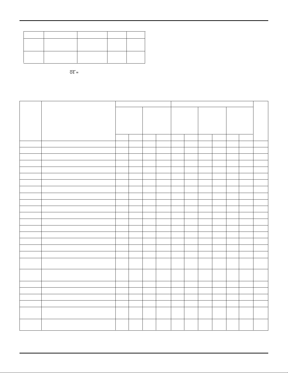
CAPACITANCE (TA = +25°C, f = 1.0MHz)
Symbol Parameter
(2)
C
IN
Input VIN = 0V 10 pF
Capacitance
(1,2)
C
OUT
Output VOUT = 0V 10 pF
Capacitance
NOTES: 2766 tbl 05
1. With output deselected, (
2. Characterized values, not currently tested.
(1)
Conditions Max. Unit
OE
= HIGH).
AC ELECTRICAL CHARACTERISTICS
(Commercial: VCC = 5V ± 10%, TA = 0°C to +70°C; Military: VCC = 5V ± 10%, TA = –55°C to +125°C)
Commercial Commercial and Military
72205LB15 72205LB20 72205LB25 72205LB35 72205LB50
72215LB15 72215LB20 72215LB25 72215LB35 72215LB50
72225LB15 72225LB20 72225LB25 72225LB35 72225LB50
72235LB15 72235LB20 72235LB25 72235LB35 72235LB50
72245LB15 72245LB20 72245LB25 72245LB35 72245LB50
Symbol Parameter Min. Max. Min. Max. Min. Max. Min. Max. Min. Max. Unit
f
S Clock Cycle Frequency — 66.7 — 50 — 40 — 28.6 — 20 MHz
t
A Data Access Time 2 10 2 12 3 15 3 20 3 25 ns
t
CLK Clock Cycle Time 15 — 20 — 25 — 35 — 50 — ns
t
CLKH Clock HIGH Time 6.5 — 8 — 10 — 14 — 20 — ns
t
CLKL Clock LOW Time 6.5 — 8 — 10 — 14 — 20 — ns
t
DS Data Set-up Time 4 — 5 — 6 — 7 — 10 — ns
t
DH Data Hold Time 1 — 1 — 1 — 2 — 2 — ns
t
ENS Enable Set-up Time 4 — 5 — 6 — 7 — 10 — ns
t
ENH Enable Hold Time 1 — 1 — 1 — 2 — 2 — ns
t
RS Reset Pulse Width
t
RSS Reset Set-up Time 10 — 12 — 15 — 20 — 30 — ns
t
RSR Reset Recovery Time 10 — 12 — 15 — 20 — 30 — ns
t
RSF Reset to Flag and Output Time — 35 — 35 — 40 — 45 — 50 ns
t
OLZ Output Enable to Output in Low-Z
t
OE Output Enable to Output Valid — 8 — 9 — 12 — 15 — 20 ns
t
OHZ Output Enable to Output in High-Z
t
WFF Write Clock to Full Flag — 10 — 12 — 15 — 20 — 30 ns
t
REF Read Clock to Empty Flag — 10 — 12 — 15 — 20 — 30 ns
t
PAF Clock to Programmable — 28 — 30 — 35 — 40 — 40 ns
Almost-Full Flag
t
PAE Clock to Programmable — 28 — 30 — 35 — 40 — 40 ns
Almost-Empty Flag
t
HF Clock to Half-Full Flag — 28 — 30 — 35 — 40 — 40 ns
t
XO Clock to Expansion Out — 10 — 12 — 15 — 20 — 30 ns
t
XI Expansion In Pulse Width 6.5 — 8 — 10 — 14 — 20 — ns
t
XIS Expansion In Set-Up Time 5 — 8 — 10 — 15 — 20 — ns
t
SKEW1 Skew time between Read Clock & 10 — 14 — 16 — 18 — 20 — ns
Write Clock for Full Flag
SKEW2 Skew time between Read Clock & 10 — 14 — 16 — 18 — 20 — ns
t
Write Clock for Empty Flag
NOTES: 2766 tbl 06
1. Pulse widths less than minimum values are not allowed.
2. Values guaranteed by design, not currently tested.
(1)
15 — 20 — 25 — 35 — 50 — ns
(2)
0—0—0— 0—0—ns
(2)
1 8 1 9 1 12 1 15 1 20 ns
5.16 6
Page 7
IDT72205LB/72215LB/72225LB/72235LB/72245LB CMOS SyncFIFO
256 x 18-BIT, 512 x 18, 1024 x 18, 2048 x 18 and 4096 x 18 MILITARY AND COMMERCIAL TEMPERATURE RANGES
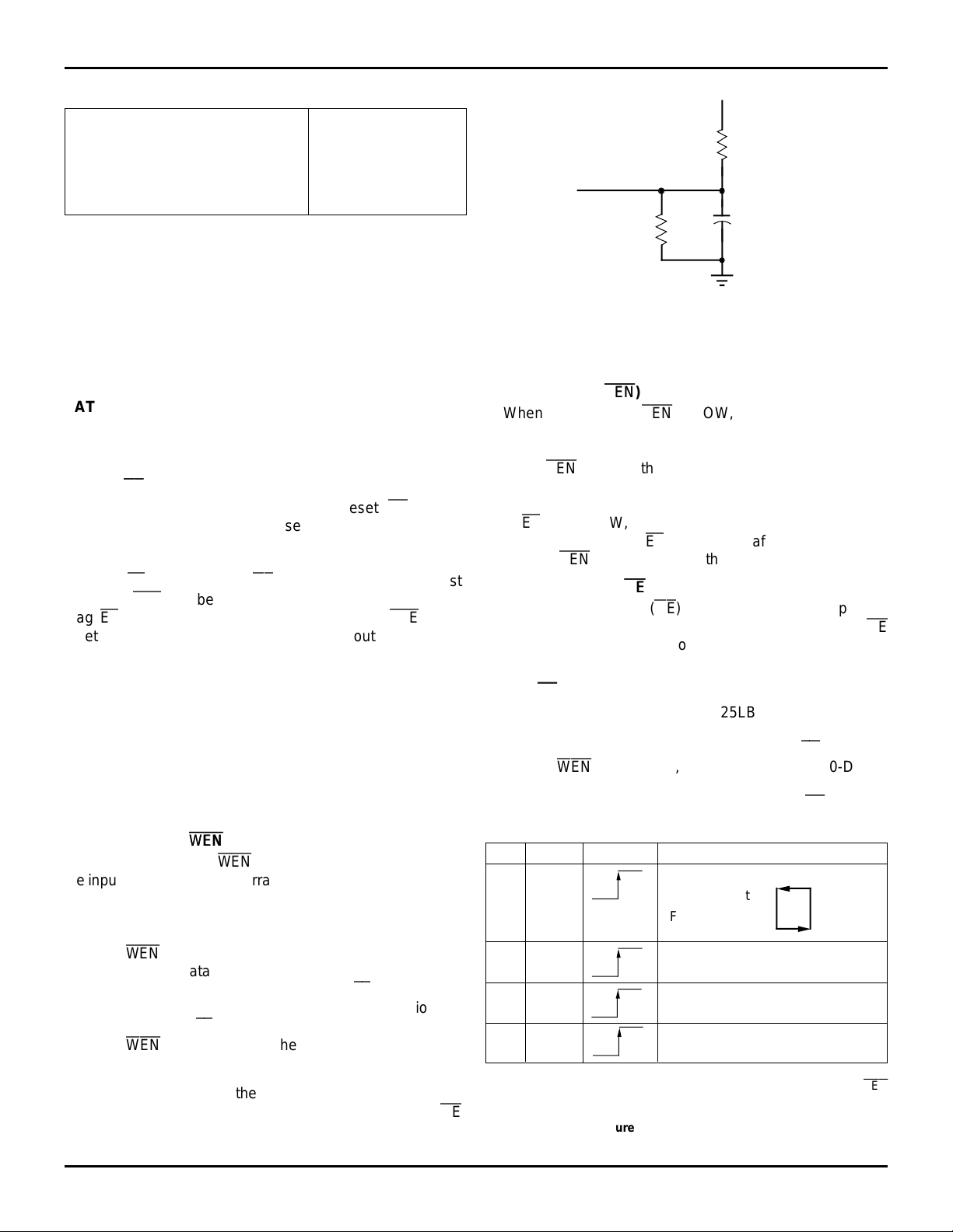
AC TEST CONDITIONS
Input Pulse Levels GND to 3.0V
Input Rise/Fall Times 3ns
Input Timing Reference Levels 1.5V
Output Reference Levels 1.5V
Output Load See Figure 1
2766 tbl 07
SIGNAL DESCRIPTIONS:
INPUTS:
DATA IN (D
Data inputs for 18-bit wide data.
CONTROLS:
RESET (
Reset is accomplished whenever the Reset (RS) input is
taken to a LOW state. During reset, both internal read and
write pointers are set to the first location. A reset is required
after power-up before a write operation can take place. The
Full Flag (FF), Half-Full Flag (HF), and Programmable AlmostFull Flag (
Flag (EF) and Programmable Almost-Empty Flag (
reset to LOW after tRSF. During reset, the output register is
initialized to all zeros and the offset registers are initialized to
their default values.
WRITE CLOCK (WCLK)
A write cycle is initiated on the LOW-to-HIGH transition of
the write clock (WCLK). Data set-up and hold times must be
met with respect to the LOW-to-HIGH transition of the write
clock (WCLK).
The write and read clocks can be asynchronous or
coincident.
0 - D17)
RSRS)
PAF
) will be reset to HIGH after t
RSF. The Empty
PAE
) will be
5V
1.1K
D.U.T.
680Ω
Figure 1. Output Load
* Includes jig and scope capacitances.
30pF*
2766 drw 05
The write and read clocks can be asynchronous or
coincident.
READ ENABLE (
When Read Enable (
REN
REN
)
REN
) is LOW, data is loaded from the
RAM array to the output register on the LOW-to-HIGH transition of the read clock (RCLK).
When
REN
is HIGH, the output register holds the previous
data and no new data is loaded into the register.
When all the data has been read from the FIFO, the Empty
Flag (EF) will go LOW, inhibiting further read operations. Once
a write is performed, the EF will go HIGH after t
can begin.
OUTPUT ENABLE (
REN
is ignored when the FIFO is empty.
OEOE)
REF and a read
When Output Enable (OE) is enabled (LOW), the parallel
output buffers receive data from the output register. When
OE
is disabled (HIGH), the Q output data bus is in a highimpedance state.
LOAD (
LDLD)
The IDT72205LB/72215LB/72225LB/72235LB/72245LB
devices contain two 12-bit offset registers with data on the
inputs, or read on the outputs. When the Load (LD) pin is set
LOW and
WEN
is set LOW, data on the inputs D0-D11 is
written into the Empty offset register on the first LOW-to-HIGH
transition of the write clock (WCLK). When the LD pin and
WRITE ENABLE (
When Write Enable (
WEN
WEN
)
WEN
) is LOW, data can be loaded into
the input register and RAM array on the LOW-to-HIGH transition of every write clock (WCLK). Data is stored in the RAM
array sequentially and independently of any on-going read
operation.
When
WEN
is HIGH, the input register holds the previous
data and no new data is loaded into the FIFO.
To prevent data overflow, the Full Flag (FF) will go LOW,
inhibiting further write operations. Upon the completion of a
valid read cycle, the FF will go HIGH after t
to begin.
WEN
is ignored when the FIFO is full.
WFF allowing a write
READ CLOCK (RCLK)
Data can be read on the outputs on the LOW-to-HIGH
transition of the read clock (RCLK), when Output Enable (OE)
is set LOW.
LD WEN WCLK
0 0 Writing to offset registers:
0 1 No Operation
1 0 Write Into FIFO
1 1 No Operation
NOTE: 2766 tbl 08
1. The same selection sequence applies to reading from the registers.
is enabled and read is performed on the LOW-to-HIGH transition of RCLK.
5.16 7
(1)
Empty Offset
Full Offset
Figure 2. Write Offset Register
Selection
REN
Page 8
IDT72205LB/72215LB/72225LB/72235LB/72245LB CMOS SyncFIFO
256 x 18, 512 x 18, 1024 x 18, 2048 x 18 and 4096 x 18 MILITARY AND COMMERCIAL TEMPERATURE RANGES
(
WEN
) are held LOW then data is written into the Full offset
register on the second LOW-to-HIGH transition of the write
clock (WCLK). The third transition of the write clock (WCLK)
again writes to the Empty offset register.
However, writing all offset registers does not have to occur
at one time. One or two offset registers can be written and then
by bringing the LD pin HIGH, the FIFO is returned to normal
read/write operation. When the LD pin is set LOW, and
WEN
is LOW, the next offset register in sequence is written.
When the LD pin is LOW and
WEN
is HIGH, the WCLK input
is disabled; then a signal at this input can neither increment the
write offset register pointer, nor execute a write.
The contents of the offset registers can be read on the
output lines when the LD pin is set LOW and
REN
is set LOW;
then, data can be read on the LOW-to-HIGH transition of the
read clock (RCLK). The act of reading the control registers
employs a dedicated read offset register pointer. (The read
and write pointers operate independently).
A read and a write should not be performed simultaneously
to the offset registers.First Load (FL)
First Load (FL) is grounded to indicate operation in the
Single Device or Width Expansion mode. In the Depth Expansion configuration, FL is grounded to indicate it is the first
device loaded and is set to HIGH for all other devices in the
daisy chain. (See Operating Configurations for further details.)
WRITE EXPANSION INPUT (
This is a dual purpose pin. Write Expansion In (
WXI
WXI
)
WXI
) is
grounded to indicate operation in the Single Device or Width
Expansion mode.
(
WXO
) of the previous device in the Depth Expansion or Daisy
WXI
is connected to Write Expansion Out
Chain mode.
READ EXPANSION INPUT (RXI)
This is a dual purpose pin. Read Expansion In (
RXI
) is
grounded to indicate operation in the Single Device or Width
Expansion mode.
(
RXO
) of the previous device in the Depth Expansion or Daisy
RXI
is connected to Read Expansion Out
Chain mode.
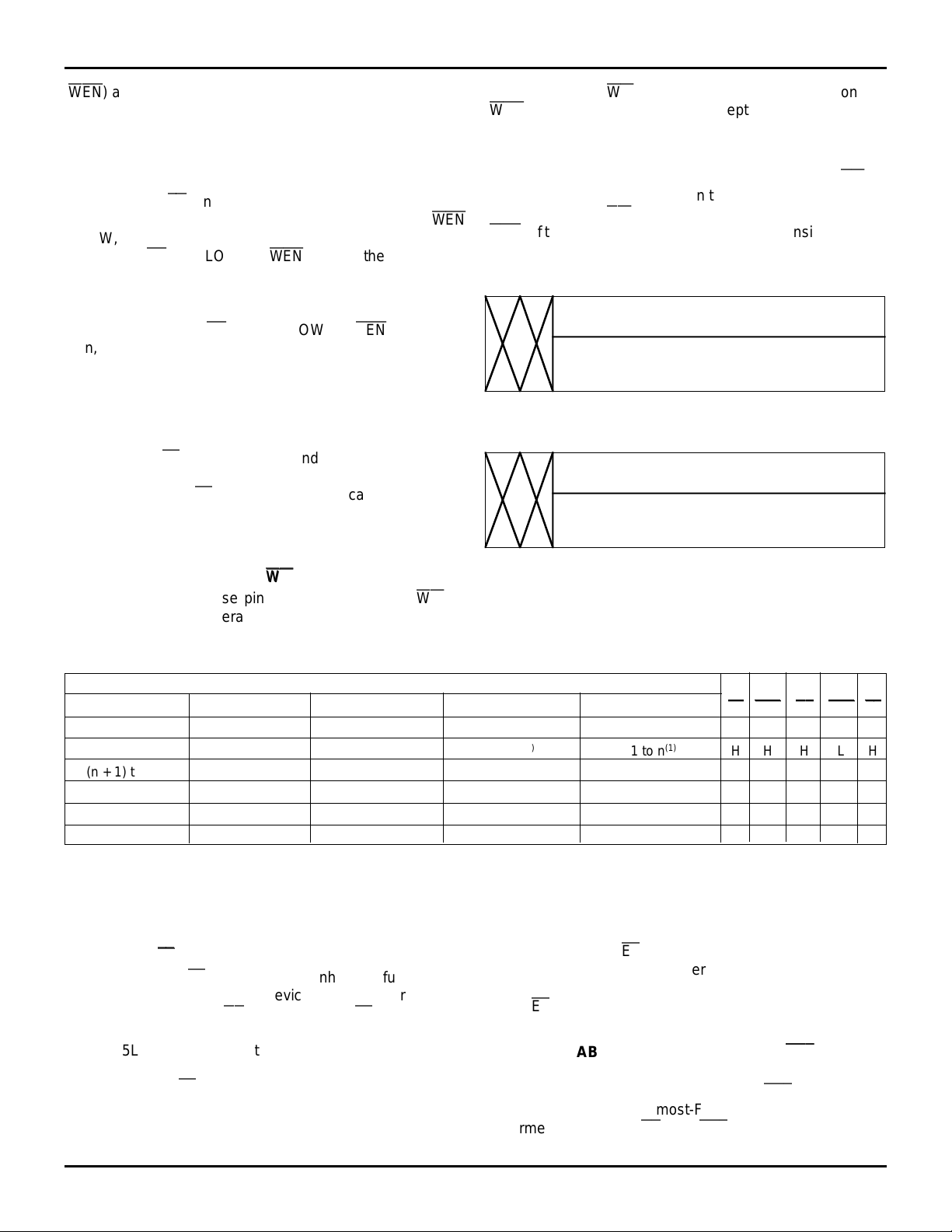
17 11 0
EMPTY OFFSET REGISTER
DEFAULT VALUE
001FH (72205) 003FH (72215):
007FH (72225/72235/72245)
17
NOTE: 2766 drw 06
1. Any bits of the offset register not being programmed should be set to zero.
11
FULL OFFSET REGISTER
DEFAULT VALUE
001FH (72205) 003FH (72215):
007FH (72225/72235/72245)
Figure 3. Offset Register Location and Default Values
0
TABLE I — STATUS FLAGS
Number of Words in FIFO
72205 72215 72225 72235 72245
00 0 0 0HHHLL
(1)
1 to n
(n + 1) to 128 (n + 1) to 256 (n + 1) to 512 (n + 1) to 1024 (n + 1) to 2048 H H H H H
129 to (256-(m+1)) 257 to (512-(m+1)) 513 to (1024-(m+1)) 1025 to (2048-(m+1)) 2049 to (4096-(m+1)) H H L H H
(256-m)
NOTES: 2766 tbl 09
1. n = Empty Offset (Default Values : 72205 n=31, 72215 n = 63, 72225/72235/72245 n = 127)
2. m = Full Offset (Default Values : 72205 n=31, 72215 n = 63, 72225/72235/72245 n = 127)
(2)
to 255 (512-m)
256 512 1024 2048 4096 L L L H H
OUTPUTS:
FULL FLAG (
FFFF)
The Full Flag (FF) will go LOW, inhibiting further write
operation, indicating that the device is full. If no reads are
performed after Reset (RS), the Full Flag (FF) will go LOW
after 256 writes for the IDT72205LB, 512 writes for the
IDT72215LB, 1024 writes for the IDT72225LB, 2048 writes for
(1)
1 to n
(2)
to 511 (1024-m)
(1)
1 to n
(2)
to 1023 (2048-m)
(1)
1 to n
(2)
to 2047 (4096-m)
(1)
1 to n
(2)
to 4095 H L L H H
EMPTY FLAG (EF)
The Empty Flag (EF) will go LOW, inhibiting further read
operations, when the read pointer is equal to the write pointer,
indicating the device is empty.
The EF is updated on the LOW-to-HIGH transition the read
clock (RCLK).
PROGRAMMABLE ALMOST-FULL FLAG (
the IDT72235LB and 4096 writes for the IDT72245LB.
The Full Flag (FF) is updated on the LOW-to-HIGH transi-
tion of the write clock (WCLK).
The Programmable Almost-Full Flag (
when FIFO reaches the Almost-Full condition. If no reads are
performed after Reset (RS), the
FFFFPAF
PAFHFHF
HH H LH
PAF
)
PAF
PAF
) will go LOW
PAF
will go LOW after (256-
PAE
PAEEFEF
5.16 8
Page 9
IDT72205LB/72215LB/72225LB/72235LB/72245LB CMOS SyncFIFO
256 x 18-BIT, 512 x 18, 1024 x 18, 2048 x 18 and 4096 x 18 MILITARY AND COMMERCIAL TEMPERATURE RANGES
m) writes for the IDT72205LB, (512-m) writes for the
IDT72215LB, (1024-m) writes for the IDT72225LB, (2048–m)
writes for the IDT72235LB and (4096–m) writes for the
IDT72245LB. The offset “m” is defined in the FULL offset
register.
If there is no Full offset specified, the
PAF
will be LOW when
the device is 31 away from completely full for 72205LB, 63
away from completely full for 72215LB, and 127 away from
completely full for 72225LB/72235LB/72245LB.
The
PAF
is asserted LOW on the LOW-to-HIGH transition
of the write clock (WCLK).
to-HIGH transition of the read clock (RCLK). Thus
PAF
is reset to HIGH on the LOW-
PAF
is
asychronous.
PROGRAMMABLE ALMOST-EMPTY FLAG (
The Programmable Almost-Empty Flag (
PAE
PAE
PAE
) will go LOW
)
when the read pointer is “n+1” locations less than the write
pointer. The offset “n” is defined in the EMPTY offset register.
If there is no Empty offset specified, the Programmable
Almost Empty Flag (
PAE
) will be LOW when the device is 31
away from completely empty for 72205LB, 63 away from
completely empty for 72215LB, and 127 away from completely empty for 72225LB/72235LB/72245LB.
The
PAE
is asserted LOW on the LOW-to-HIGH transition
of the read clock (RCLK).
to-HIGH transition of the write clock (WCLK). Thus
PAE
is reset to HIGH on the LOW-
PAF
is
asychronous.
WRITE EXPANSION OUT/HALF-FULL FLAG (
WXO
WXO
/
HFHF)
This is a dual-purpose output. In the Single Device and
Width Expansion mode, when Write Expansion In (
WXI
) is
grounded, this output acts as an indication of a half-full
memory.
After half of the memory is filled, and at the LOW-to-HIGH
transition of the next write cycle, the Half-Full Flag goes LOW
and will remain set until the difference between the write
pointer and read pointer is less than or equal to one half of the
total memory of the device. The Half-Full Flag (HF) is then reset
to HIGH by the LOW-to-HIGH transition of the read clock
(RCLK). The HF is asychronous.
In the Depth Expansion or Daisy Chain mode,
connected to
WXO
of the previous device. This output acts as
WXI
is
a signal to the next device in the Daisy Chain by providing a
pulse when the previous device writes to the last location of
memory.
READ EXPANSION OUT (
RXO
RXO
)
In the Depth Expansion or Daisy Chain configuration, Read
Expansion In (
(
RXO
) of the previous device. This output acts as a signal to
RXI
) is connected to Read Expansion Out
the next device in the Daisy Chain by providing a pulse when
the previous device reads from the last location of memory.
DATA OUTPUTS (Q0-Q17)
Q0-Q17 are data outputs for 18-bit wide data.
t
t
t
t
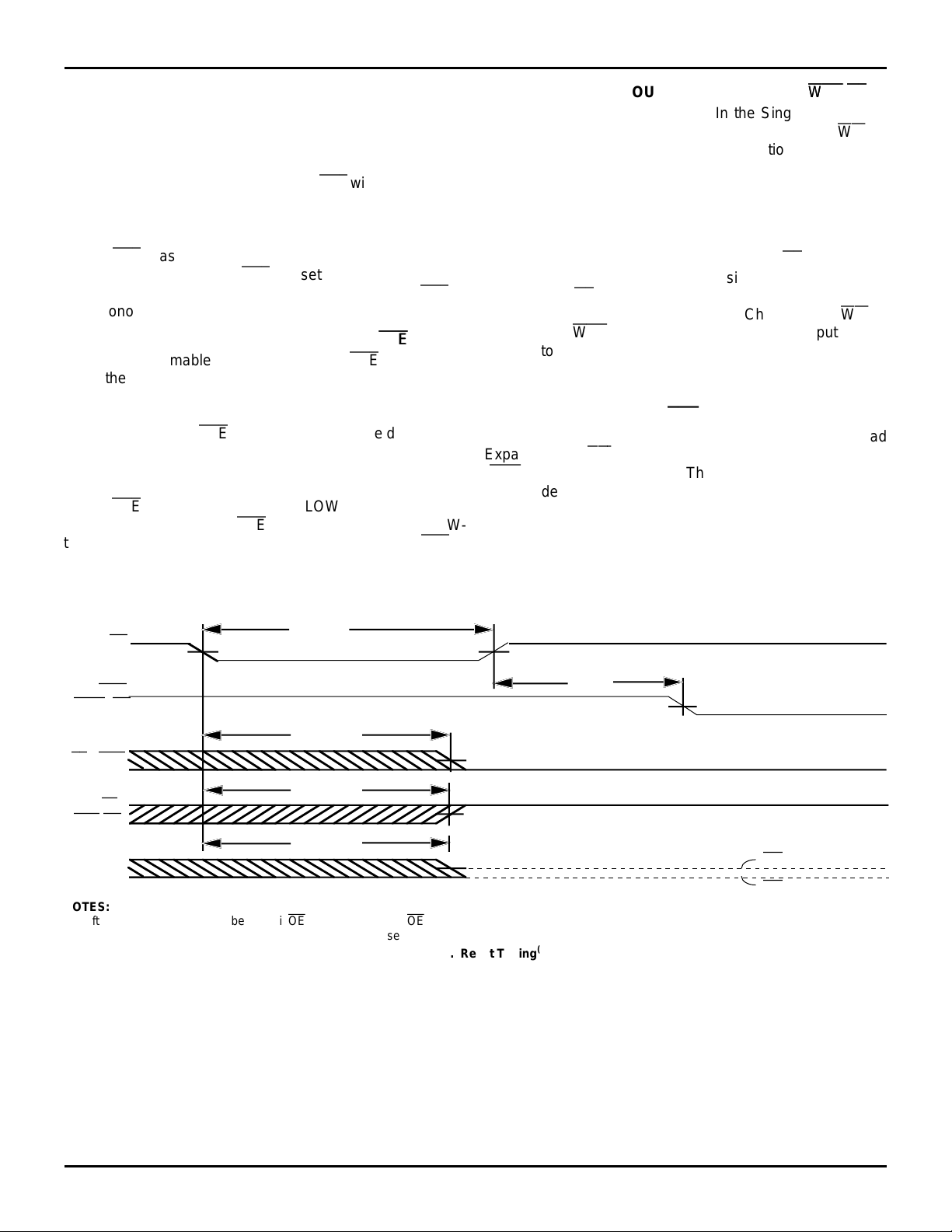
RS
RSF
RSF
RSF
Figure 5. Reset Timing
RS
REN
,
PAE
FF
,
,
WEN, LD
EF
PAF,HF
Q0 - Q17
NOTES:
1. After reset, the outputs will be LOW if OE = 0 and tri-state if OE = 1.
2. The clocks (RCLK, WCLK) can be free-running during reset.
t
RSR
(1)
OE
= 1
OE
= 0
(2)
5.16 9
Page 10
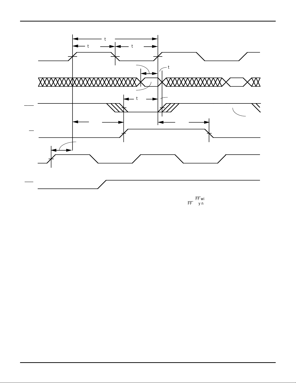
IDT72205LB/72215LB/72225LB/72235LB/72245LB CMOS SyncFIFO
256 x 18, 512 x 18, 1024 x 18, 2048 x 18 and 4096 x 18 MILITARY AND COMMERCIAL TEMPERATURE RANGES
t
CLK
tt
CLKH CLKL
WCLK
t
DS
t
DH
D0 - D17
DATA IN VALID
t
ENH
WEN
t
ENS
tt
WFF WFF
FF
(1)
t
SKEW1
RCLK
REN
NOTE:
1. tSKEW1 is the minimum time between a rising RCLK edge and a rising WCLK edge to guarantee that
the time between the rising edge of RCLK and the rising edge of WCLK is less than t
SKEW1, then
FF
NO OPERATION
2766 drw 08
FF
will go HIGH during the current clock cycle. If
may not change state until the next WCLK edge.
Figure 6. Write Cycle Timing
5.16 10
Page 11
IDT72205LB/72215LB/72225LB/72235LB/72245LB CMOS SyncFIFO
256 x 18-BIT, 512 x 18, 1024 x 18, 2048 x 18 and 4096 x 18 MILITARY AND COMMERCIAL TEMPERATURE RANGES
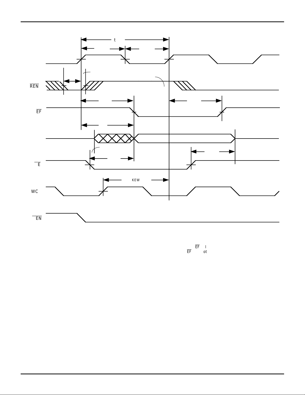
t
CLK
tt
CLKH CLKL
RCLK
REN
EF
Q0 - Q17
OE
WCLK
t
ENS
t
ENH
t
REF
t
A
t
OLZ
NO OPERATION
t
REF
VALID DATA
t
OHZ
t
OE
(1)
t
SKEW2
WEN
NOTE:
1. t
SKEW2 is the minimum time between a rising WCLK edge and a rising RCLK edge to guarantee that
time between the rising edge of WCLK and the rising edge of RCLK is less than t
Figure 7. Read Cycle Timing
SKEW2, then
EF
will go HIGH during the current clock cycle. If the
EF
may not change state until the next RCLK edge.
2766 drw 09
5.16 11
Page 12
IDT72205LB/72215LB/72225LB/72235LB/72245LB CMOS SyncFIFO
256 x 18, 512 x 18, 1024 x 18, 2048 x 18 and 4096 x 18 MILITARY AND COMMERCIAL TEMPERATURE RANGES
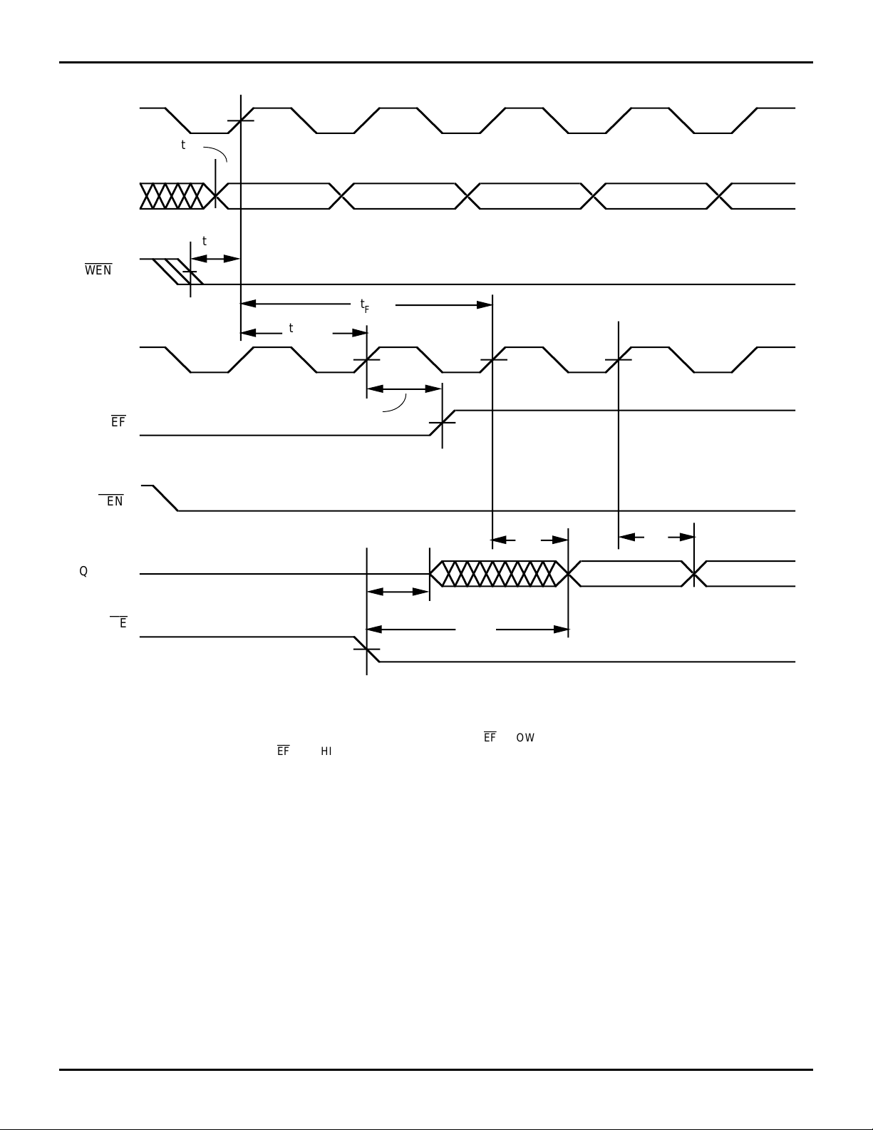
WCLK
t
DS
D
D0 - D17
t
ENS
(first valid write)
0
DDD
12 3
D
4
WEN
(1)
t
FRL
t
SKEW2
RCLK
t
EF
REF
REN
0 - Q17
Q
t
OLZ
OE
NOTES:
1. When t
2. The first word is available the cycle after EF goes HIGH, always.
SKEW2 ≥ minimum specification, tFRL (maximum) = tCLK + tSKEW2. When tSKEW2 < minimum specification, tFRL (maximum) = either 2 * tCLK +
SKEW2 or tCLK + tSKEW2. The Latency Timing applies only at the Empty Boundary (
t
Figure 8. First Data Word Latency after Reset with Simultaneous Read and Write
t
A
t
OE
EF
= LOW).
t
A
DD
01
2766 drw 10
5.16 12
Page 13
IDT72205LB/72215LB/72225LB/72235LB/72245LB CMOS SyncFIFO
256 x 18-BIT, 512 x 18, 1024 x 18, 2048 x 18 and 4096 x 18 MILITARY AND COMMERCIAL TEMPERATURE RANGES
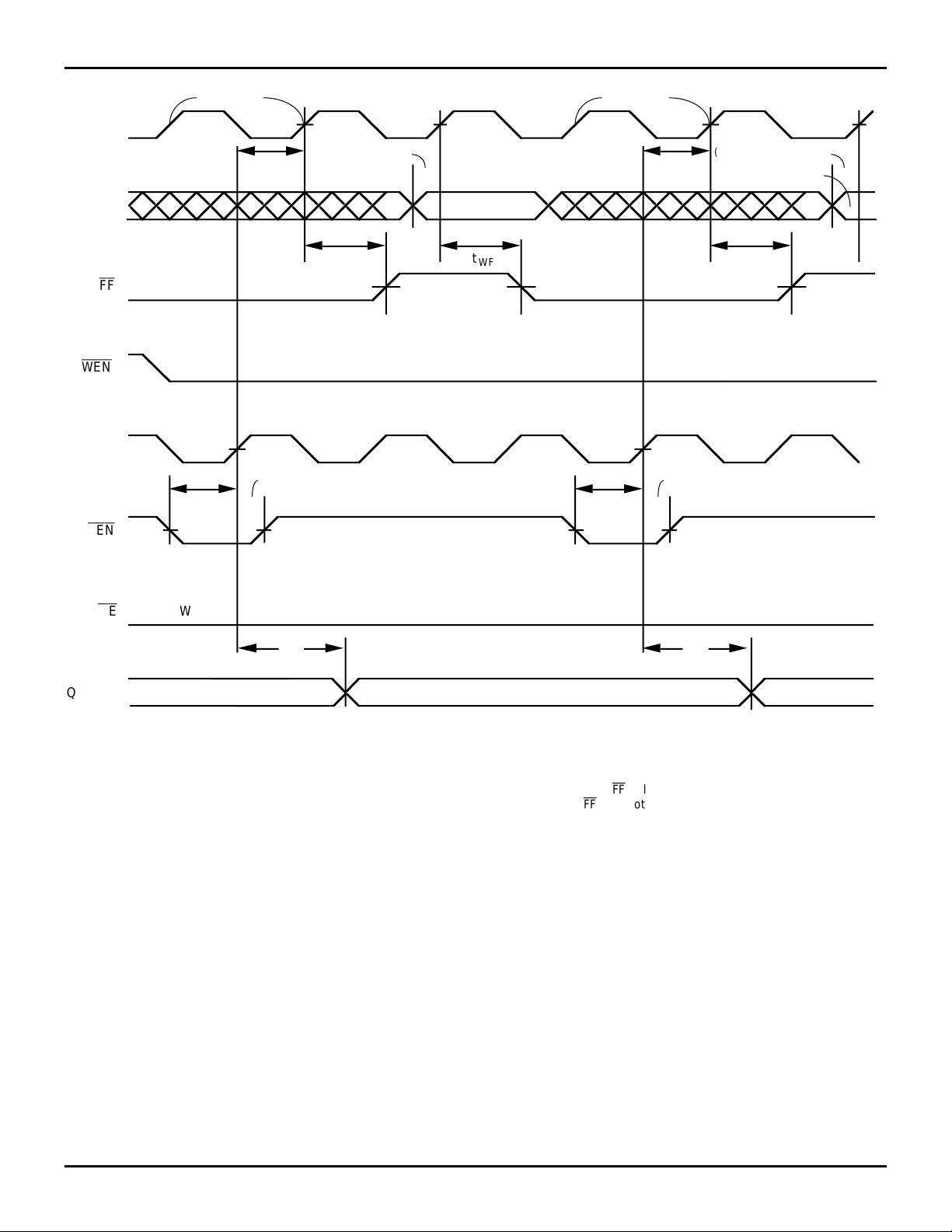
NO WRITE NO WRITE
WCLK
D0 - D
t
SKEW1
17
(1)
t
DS
t
SKEW1
DATA WRITE
(1)
DATA WRITE
t
DS
Q
0
FF
WEN
RCLK
REN
OE
- Q
17
t
ENH
t
ENS
LOW
t
A
DATA IN OUTPUT REGISTER
t
WFF
t
WFF
DATA READ
t
ENS
t
ENH
t
WFF
t
A
NEXT DATA READ
Figure 9. Full Flag Timing
NOTE:
1. t
SKEW1 is the minimum time between a rising RCLK edge and a rising WCLK edge to guarantee that
time between the rising edge of RCLK and the rising edge of WCLK is less than t
SKEW1, then
FF
will go HIGH during the current clock cycle. If the
FF
may not change state until the next WCLK edge.
2766 drw 11
5.16 13
Page 14
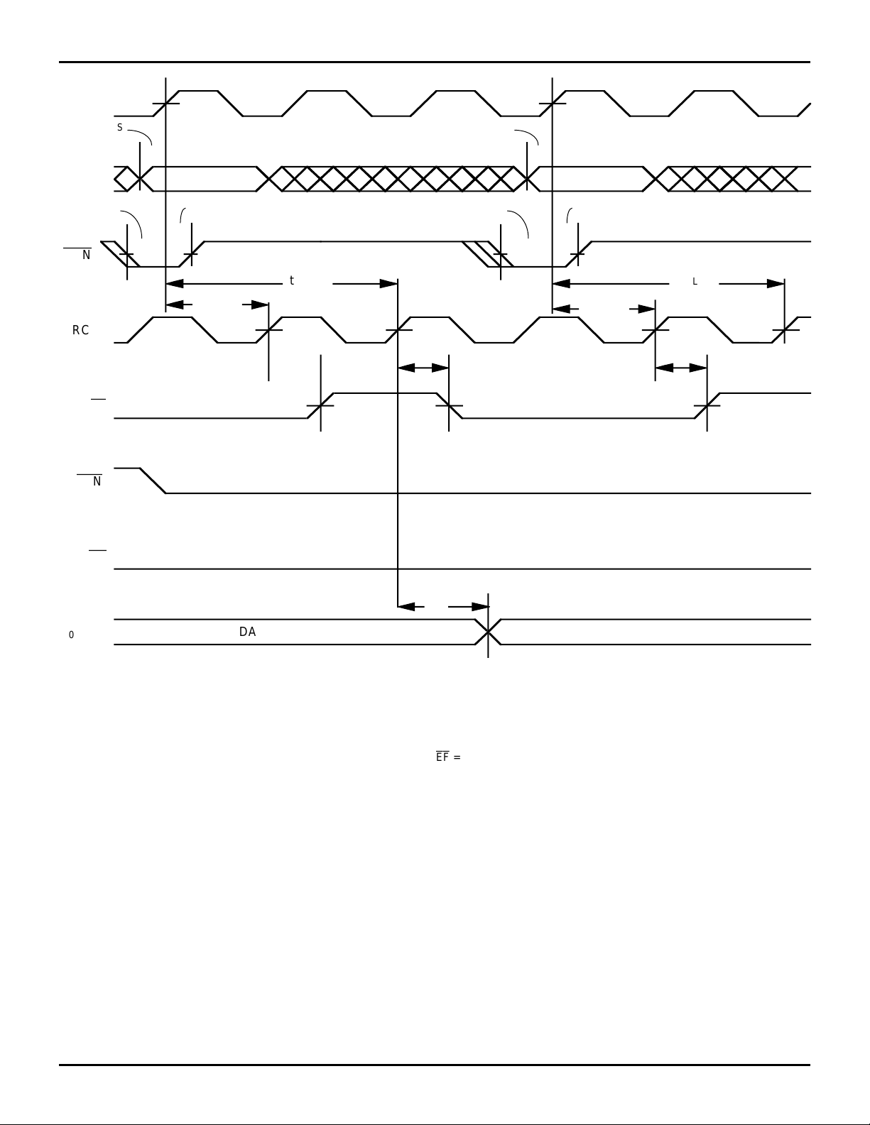
IDT72205LB/72215LB/72225LB/72235LB/72245LB CMOS SyncFIFO
256 x 18, 512 x 18, 1024 x 18, 2048 x 18 and 4096 x 18 MILITARY AND COMMERCIAL TEMPERATURE RANGES
WCLK
tDS
tDS
D0 - D17
tENS
WEN
RCLK
EF
REN
OE
DATA WRITE 1
tENH
tSKEW2
LOW
tFRL
(1)
tREF
tENS
DATA WRITE 2
tENH
tSKEW2
tFRL
tREF
(1)
0 - Q17
Q
NOTE:
1. When t
SKEW2 ≥ minimum specification, tFRL (maximum) = tCLK + tSKEW2. When tSKEW2 < minimum specification, tFRL (maximum) = either 2 * tCLK + tSKEW2.
tCLK + tSKEW2. The Latency Timing apply only at the Empty Boundary (EF = LOW).
or
DATA IN OUTPUT REGISTER
Figure 10. Empty Flag Timing
tA
DATA READ
2766 drw 12
5.16 14
Page 15
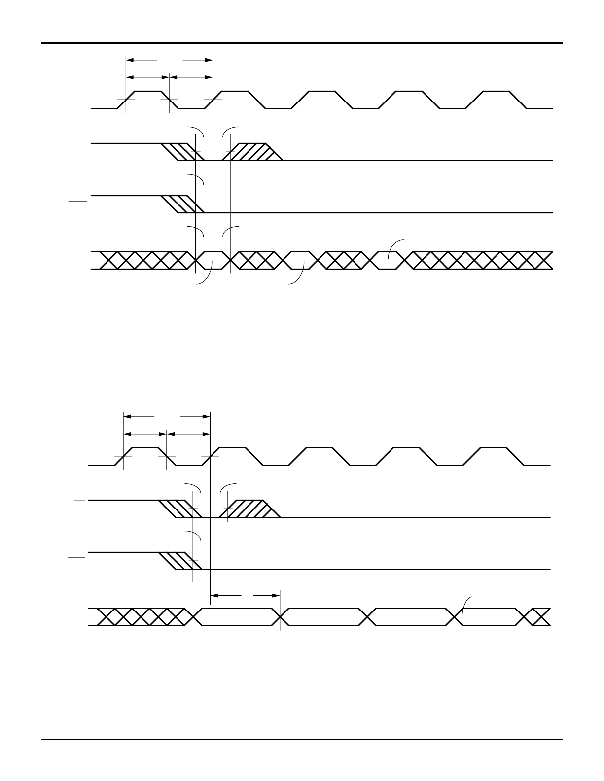
IDT72205LB/72215LB/72225LB/72235LB/72245LB CMOS SyncFIFO
256 x 18-BIT, 512 x 18, 1024 x 18, 2048 x 18 and 4096 x 18 MILITARY AND COMMERCIAL TEMPERATURE RANGES
tCLK
tCLKH tCLKL
WCLK
tENS tENH
LD
tENS
WEN
tDS tDH
PAE OFFSET
D0–D15
RCLK
LD
REN
PAE OFFSET PAF OFFSET
Figure 11. Write Programmable Registers
tCLK
tCLKH tCLKL
tENS tENH
tENS
D0–D11
2766 drw 13
Q0–Q15
tA
UNKNOWN
Figure 12. Read Programmable Registers
PAE OFFSET PAF OFFSET
5.16 15
PAE OFFSET
2766 drw 14
Page 16
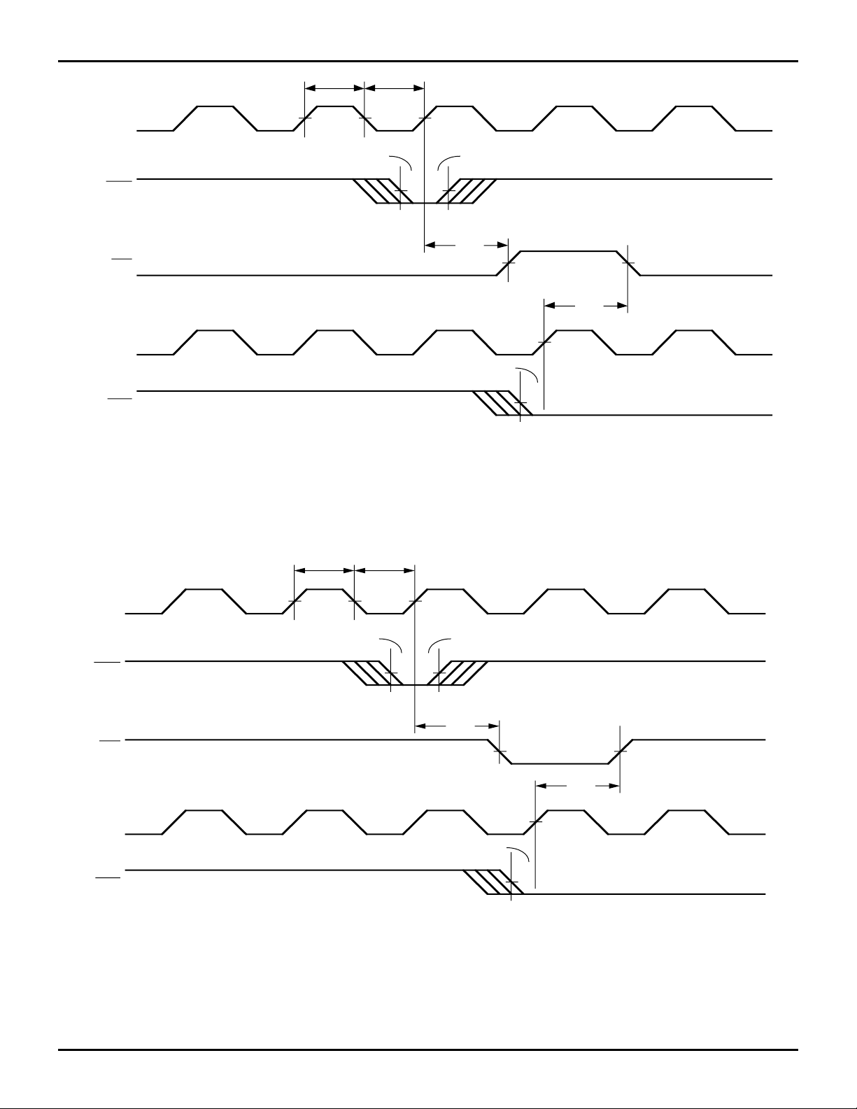
IDT72205LB/72215LB/72225LB/72235LB/72245LB CMOS SyncFIFO
256 x 18, 512 x 18, 1024 x 18, 2048 x 18 and 4096 x 18 MILITARY AND COMMERCIAL TEMPERATURE RANGES
t
CLKH
t
CLKL
WCLK
t
ENS
t
ENH
WEN
t
PAE
PAE
n + 1 words
in FIFO
t
PAE
n words in FIFO
RCLK
t
ENS
REN
NOTE:
1. PAE is offset = n. Number of data words written into FIFO already = n.
Figure 13. Programmable Almost Empty Flag Timing
tCLKH tCLKL
WCLK
(1)
tENS tENH
WEN
PAF
RCLK
tPAF
tENS
Full – m words
in FIFO(2)
tPAF
2766 drw 15
Full – m + 1 words
in FIFO(3)
REN
2766 drw 16
NOTES:
1. PAF offset = m. Number of data words written into FIFO already = 256 - m + 1 for the IDT72205B, 512 - m + 1 for the IDT72215B, 1024 - m + 1 for the
IDT72225B, 2048 – m + 1 for the IDT72235B and 4096 – m +1 for the IDT72245B.
2. 256 - m words in IDT72205B, 512 - m words in IDT72215B, 1024 - m words in IDT72225B, 2048 – m words in IDT72235B and 4096 – m words in IDT72245B.
3. 256 - m + 1 words in IDT72205B, 512 - m + 1 words in IDT72215B, 1024 - m + 1 words in IDT72225B, 2048 – m + 1 words in IDT72235B and 4096 – m
+ 1 words in IDT72245B.
Figure 14. Programmable Almost-Full Flag Timing
5.16 16
Page 17
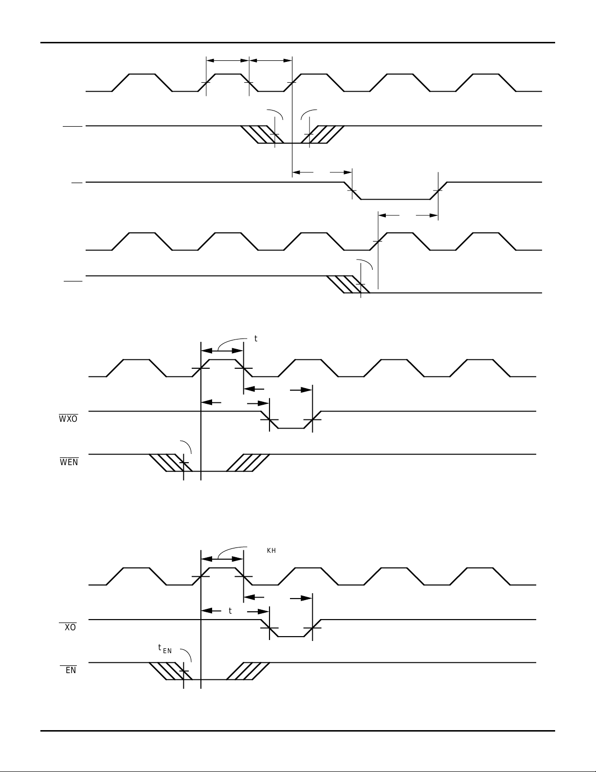
IDT72205LB/72215LB/72225LB/72235LB/72245LB CMOS SyncFIFO
256 x 18-BIT, 512 x 18, 1024 x 18, 2048 x 18 and 4096 x 18 MILITARY AND COMMERCIAL TEMPERATURE RANGES
tCLKH tCLKL
WCLK
tENS tENH
WEN
HF
RCLK
REN
WCLK
WXO
Half Full or Less
t
ENS
Note 1
tHF
Figure 15. Half-Full Flag Timing
t
CLKH
t
XO
t
XO
tENS
Half Full + 1
or More
tHF
Half Full or Less
2766 drw 17
WEN
NOTE:
1. Write to Last Physical Location.
RCLK
RXO
t
REN
NOTE:
1. Read from Last Physical Location.
ENS
Figure 16. Write Expansion Out Timing
t
CLKH
Note 1
t
XO
Figure 17. Read Expansion Out Timing
t
XO
5.16 17
2766 drw 18
2766 drw 19
Page 18
IDT72205LB/72215LB/72225LB/72235LB/72245LB CMOS SyncFIFO
256 x 18, 512 x 18, 1024 x 18, 2048 x 18 and 4096 x 18 MILITARY AND COMMERCIAL TEMPERATURE RANGES
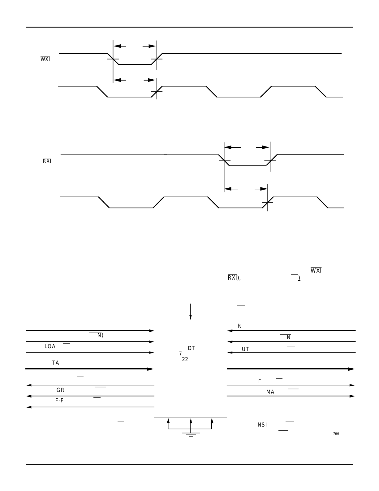
t
XI
WXI
t
XIS
WCLK
2766 drw 20
Figure 18. Write Expansion In Timing
t
XI
RXI
t
XIS
RCLK
Figure 19. Read Expansion In Timing
OPERATING CONFIGURATIONS
SINGLE DEVICE CONFIGURATION
A single IDT72205LB/72215LB/72225LB/72235LB/
72245LB may be used when the application requirements are
for 256/512/1024/2048/4096 words or less. The IDT72205LB/
WRITE CLOCK (WCLK)
WRITE ENABLE (
LOAD (LD)
DATA IN (D
FULL FLAG (FF)
PROGRAMMABLE (
HALF-FULL FLAG (HF)
0 - D17)
WEN
PAE
)
72205LB/
72215LB/
72225LB/
72235LB/
72245LB
)
2766 drw 21
72215LB/72225LB/72235LB/72245LB are in a single Device
Configuration when the Write Exansion In (
pansion In (
RXI
), and First Load (FL) control inputs are
WXI
), Read Ex-
grounded (Figure 20).
RESET (RS)
READ CLOCK (RCLK)
IDT
READ ENABLE (
OUTPUT ENABLE (OE)
DATA OUT (Q
EMPTY FLAG (EF)
PROGRAMMABLE (
REN
0 - Q17)
)
PAF
)
FIRST LOAD (FL)
READ EXPANSION IN (
WRITE EXPANSION IN (
Figure 20. Block Diagram of Single 256 x 18/512 x 18/1024 x 18/2048 x 18/4096 x 18 Synchronous FIFO
5.16 18
WXI
RXI
)
)
2766 drw 22
Page 19
IDT72205LB/72215LB/72225LB/72235LB/72245LB CMOS SyncFIFO
256 x 18-BIT, 512 x 18, 1024 x 18, 2048 x 18 and 4096 x 18 MILITARY AND COMMERCIAL TEMPERATURE RANGES
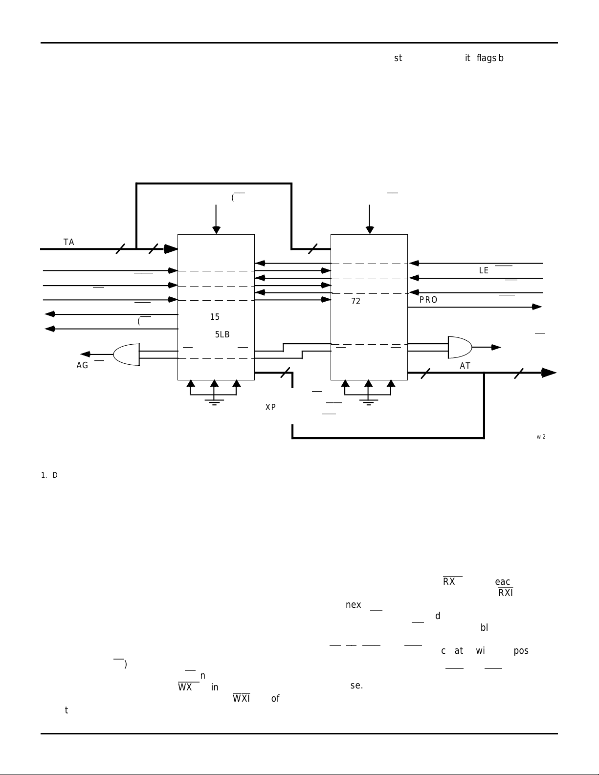
WIDTH EXPANSION CONFIGURATION
Word width may be increased simply by connecting to-
gether the control signals of multiple devices. Status flags can
be detected from any one device. The exceptions are the
Empty Flag and Full Flag. Because of variations in skew
between RCLK and WCLK, it is possible for flag assertion and
deassertion to vary by one cycle between FIFOs. To avoid
RESET (RS)
DATA IN (D)
WRITE CLOCK (WCLK)
WRITE ENABLE (
LOAD (LD)
PROGRAMMABLE (
HALF FULL FLAG (HF)
FULL FLAG (FF)
36
18 18
WEN
)
PAE
)
72205LB/
72215LB/
72225LB/
72235LB/
72245LB
FF FF EFEF
18
FIRST LOAD (FL)
WRITE EXPANSION IN (
READ EXPANSION IN (
problems the user must create composite flags by ANDing the
Empty Flags of every FIFO, and separately ANDing all Full
Flags. Figure 21 demonstrates a 36-word width by using two
IDT72205B/72215B/72225B/72235B/72245Bs. Any word
width can be attained by adding additional IDT72205B/72215B/
72225B/72235B/72245Bs. Please see the Application Note
AN-83.
RESET (RS)
READ CLOCK (RCLK)
WXI
RXI
)
)
72205LB/
72215LB/
72225LB/
72235LB/
72245LB
READ ENABLE (
OUTPUT ENABLE (OE)
PROGRAMMABLE (
18
DATA OUT (Q)
REN
)
PAF
)
EMPTY FLAG (EF)
36
NOTE:
1. Do not connect any output control signals directly together.
Figure 21. Block Diagram of 256 x 36/512 x 36/1024 x 36/2048 x 36/4096 x 36 Synchronous FIFO Memory Used in a
Width Expansion Configuration
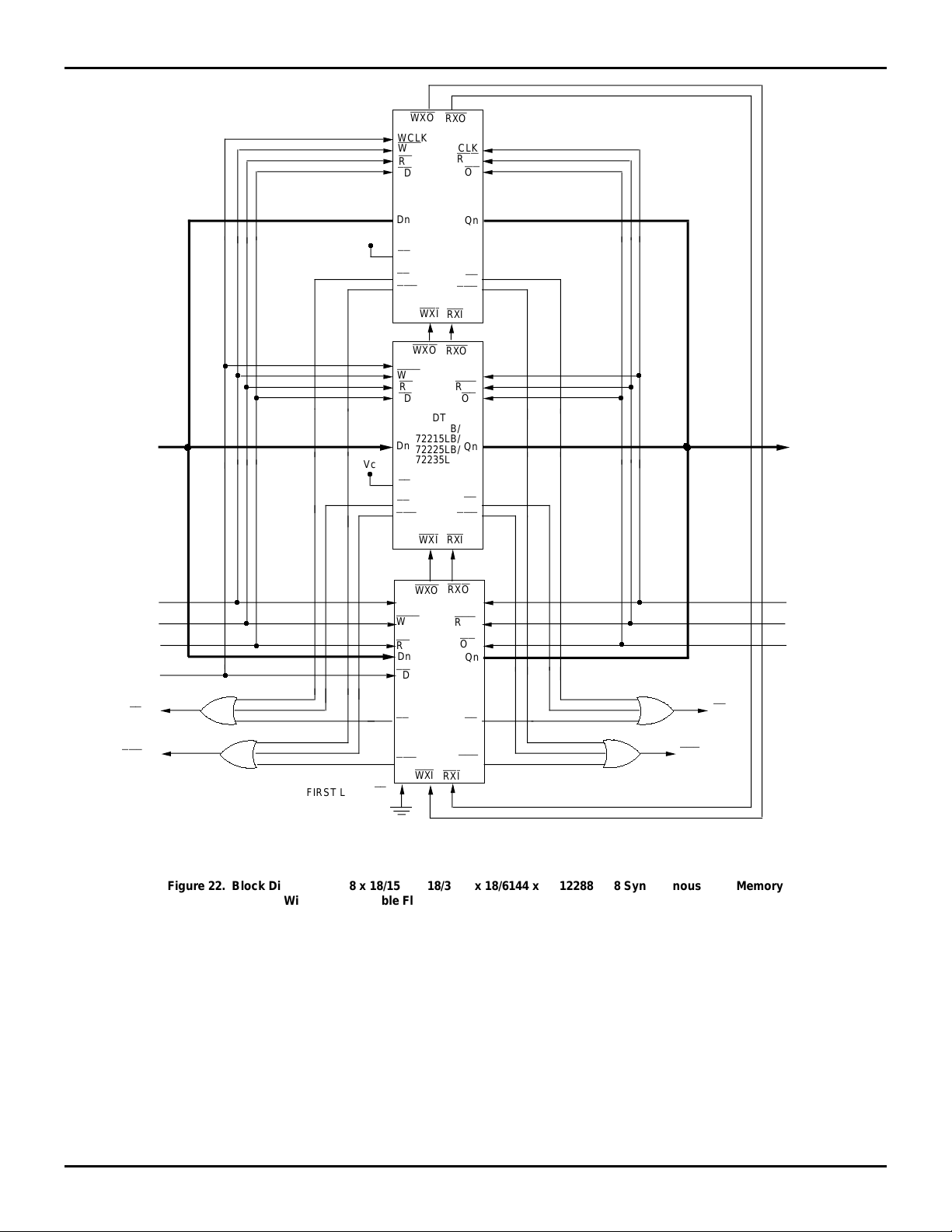
DEPTH EXPANSION CONFIGURATION
(WITH PROGRAMMABLE FLAGS)
The IDT72205LB/72215LB/72225LB/72235LB/72245LB can
easily be adapted to applications requiring more than 256/
512/1024/2048/4096 words of buffering. Figure 22 shows
Depth Expansion using three IDT72205LB/72215LB/72225LB/
72235LB/72245LBs. Maximum depth is limited only by signal
loading. Follow these steps:
1. The first device must be designated by grounding the
First Load (FL) control input.
2. All other devices must have FL in the HIGH state.
3. The Write Expansion Out (
must be tied to the Write Expansion In (
WXO
) pin of each device
WXI
) pin of
the next device. See Figure 24.
2766 drw 23
4. The Read Expansion Out (
must be tied to the Read Expansion In (
RXO
) pin of each device
RXI
) pin of
the next device. See Figure 24.
5. All Load (LD) pins are tied together.
6. The Half-Full Flag (HF) is not available in the Depth
Expansion Configuration.
7.EF, FF,
PAE
, and
PAF
are created with composite
flags by ORing together every respective flags for
monitoring. The composite
PAE
and
PAF
flags are not
precise.
5.16 19
Page 20
IDT72205LB/72215LB/72225LB/72235LB/72245LB CMOS SyncFIFO
256 x 18, 512 x 18, 1024 x 18, 2048 x 18 and 4096 x 18 MILITARY AND COMMERCIAL TEMPERATURE RANGES
WXO
RXO
WCLK
DATA IN
WEN
RS
LD
Dn
Vcc
•
FL
FF
PAF
Vcc
•
WCLK
WEN
RS
LD
Dn
FL
FF
PAF
•
•
•
•
IDT
72205LB/
72215LB/
72225LB/
72235LB/
72245LB
WXI
WXO
IDT
72205LB/
72215LB/
72225LB/
72235LB/
72245LB
WXI
RCLK
REN
PAE
RXI
RXO
RCLK
REN
PAE
RXI
OE
Qn
Qn
EF
OE
EF
•
•
•
•
DATA OUT
WRITE CLOCK
WRITE ENABLE
RESET
LOAD
FF
PAF
•
•
•
•
FIRST LOAD (FL)
WCLK
WEN
RS
Dn
72205LB/
LD
72215LB/
72225LB/
72235LB/
72245LB
FF
PAF
WXI
IDT
RCLK
RXI
REN
OE
PAE
•
•
Qn
EF
•
EF
PAE
2766 drw 24
RXO
WXO
Figure 22. Block Diagram of 768 x 18/1536 x 18/3072 x 18/6144 x 18/12288 x 18 Synchronous FIFO Memory
With Programmable Flags used in Depth Expansion Configuration
READ CLOCK
READ ENABLE
OUTPUT ENABLE
5.16 20
Page 21
IDT72205LB/72215LB/72225LB/72235LB/72245LB CMOS SyncFIFO
256 x 18-BIT, 512 x 18, 1024 x 18, 2048 x 18 and 4096 x 18 MILITARY AND COMMERCIAL TEMPERATURE RANGES
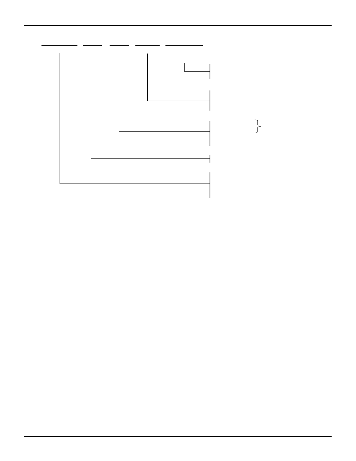
ORDERING INFORMATION
IDT XXXXX
Device TypeXPowerXXSpeed
X
Package
X
Process /
Temperature
Range
BLANK
B
Commercial (0°C to +70°C)
Military (–55°C to +125°C)
Compliant to MIL-STD-883, Class B
J
G
PF
TF
15 Com'l Only
20 Com'l Only
Plastic Leaded Chip Carrier
Pin Grid Array
Thin Plastic Quad Flatpack
Slim Thin Plastic Quad Flatpack
25
35
50
LB
72205
72215
72225
72235
72245
Low Power
256 x 18 Synchronous FIFO
512 x 18 Synchronous FIFO
1024 x 18 Synchronous FIFO
2048 x 18 Synchronous FIFO
4096 x 18 Synchronous FIFO
Clock Cycle Time (tCLK)
Speed in Nanoseconds
2766 drw 25
5.16 21
 Loading...