

查询IDT72255L10G供应商
CMOS SUPERSYNC FIFO
8,192 x 18, 16,384 x 18
Integrated Device Technology, Inc.
FEATURES:
• 8,192 x 18-bit storage capacity (IDT72255)
• 16,384 x 18-bit storage capacity (IDT72265)
• 10ns read/write cycle time (8ns access time)
• Retransmit Capability
• Auto power down reduces power consumption
• Master Reset clears entire FIFO, Partial Reset clears
data, but retains programmable settings
• Empty, Full and Half-full flags signal FIFO status
• Programmable Almost Empty and Almost Full flags, each
flag can default to one of two preselected offsets
• Program partial flags by either serial or parallel means
• Select IDT Standard timing (using EF and FF flags) or
First Word Fall Through timing (using OR and IR flags)
• Easily expandable in depth and width
• Independent read and write clocks (permit simultaneous
reading and writing with one clock signal)
• Available in the 64-pin Thin Quad Flat Pack (TQFP), 64pin Slim Thin Quad Flat Pack (STQFP) and the 68-pin
Pin Grid Array (PGA)
• Output enable puts data outputs into high impedance
• High-performance submicron CMOS technology
• Industrial temperature range (-40
able, tested to military electrical specifications
o
C to +85oC) is avail-
IDT72255
IDT72265
DESCRIPTION:
The IDT72255/72265 are monolithic, CMOS, high capacity, high speed, low power First-In, First-Out (FIFO) memories
with clocked read and write controls. These FIFOs are applicable for a wide variety of data buffering needs, such as optical
disk controllers, local area networks (LANs), and inter-processor communication.
Both FIFOs have an 18-bit input port (Dn) and an 18-bit
output port (Qn). The input port is controlled by a free-running
clock (WCLK) and a data input enable pin (
written into the synchronous FIFO on every clock when
is asserted. The output port is controlled by another clock pin
(RCLK) and enable pin (
REN
). The read clock can be tied to
the write clock for single clock operation or the two clocks can
run asynchronously for dual clock operation. An output enable
pin (OE) is provided on the read port for three-state control of
the outputs.
The IDT72255/72265 have two modes of operation: In the
IDT Standard Mode
, the first word written to the FIFO is
deposited into the memory array. A read operation is required
to access that word. In the
First Word Fall Through Mode
(FWFT), the first word written to an empty FIFO appears
WEN
). Data is
WEN
FUNCTIONAL BLOCK DIAGRAM
WEN
WCLK
•
WRITE CONTROL
LOGIC
WRITE POINTER
MRS
PRS
FS
RESET
LOGIC
TIMING
0-D17
D
•
INPUT REGISTER
RAM ARRAY
8,192 x 18
16,384 x 18
OUTPUT REGISTER
•
Q
OE
•
•
•
•
0-Q17
OFFSET REGISTER
READ POINTER
LD
FLAG
LOGIC
READ
CONTROL
LOGIC
•
3037 drw 01
SEN
•
RCLK
REN
FF/IR
PAF
EF/OR
PAE
HF
FWFT/SI
RT
SyncFIFO is a trademark and the IDT logo is a registered trademark of Integrated Device Technology, Inc.
MILITARY AND COMMERCIAL TEMPERATURE RANGES MAY 1997
1997 Integrated Device Technology, Inc DSC-3037/7
For latest information contact IDT's web site at www.idt.com or fax-on-demand at 408-492-8391.
1
IDT72255/72265 SyncFIFO
8,192 x 18, 16,384 x 18
MILITARY AND COMMERCIAL TEMPERATURE RANGES
automatically on the outputs, no read operation required. The
state of the FWFT/SI pin during Master Reset determines the
mode in use.
The IDT72255/72265 FIFOs have five flag functions, EF/
OR
(Empty Flag or Output Ready), FF/IR (Full Flag or Input
Ready), and HF (Half-full Flag). The EF and FF functions are
selected in the IDT Standard Mode.
The IR and OR functions are selected in the First Word Fall
Through Mode. IR indicates that the FIFO has free space to
receive data. OR indicates that data contained in the FIFO is
available for reading.
HF
is a flag whose threshold is fixed at the half-way point in
memory. This flag can always be used irrespective of mode.
PAE, PAF
can be programmed independantly to any point
in memory. They, also, can be used irrespective of mode.
Programmable offsets determine the flag threshold and can
be loaded by two methods: parallel or serial. Two default
offset settings are also provided, such that
127 or 1023 locations from the empty boundary and the
PAE
can be set at
PAF
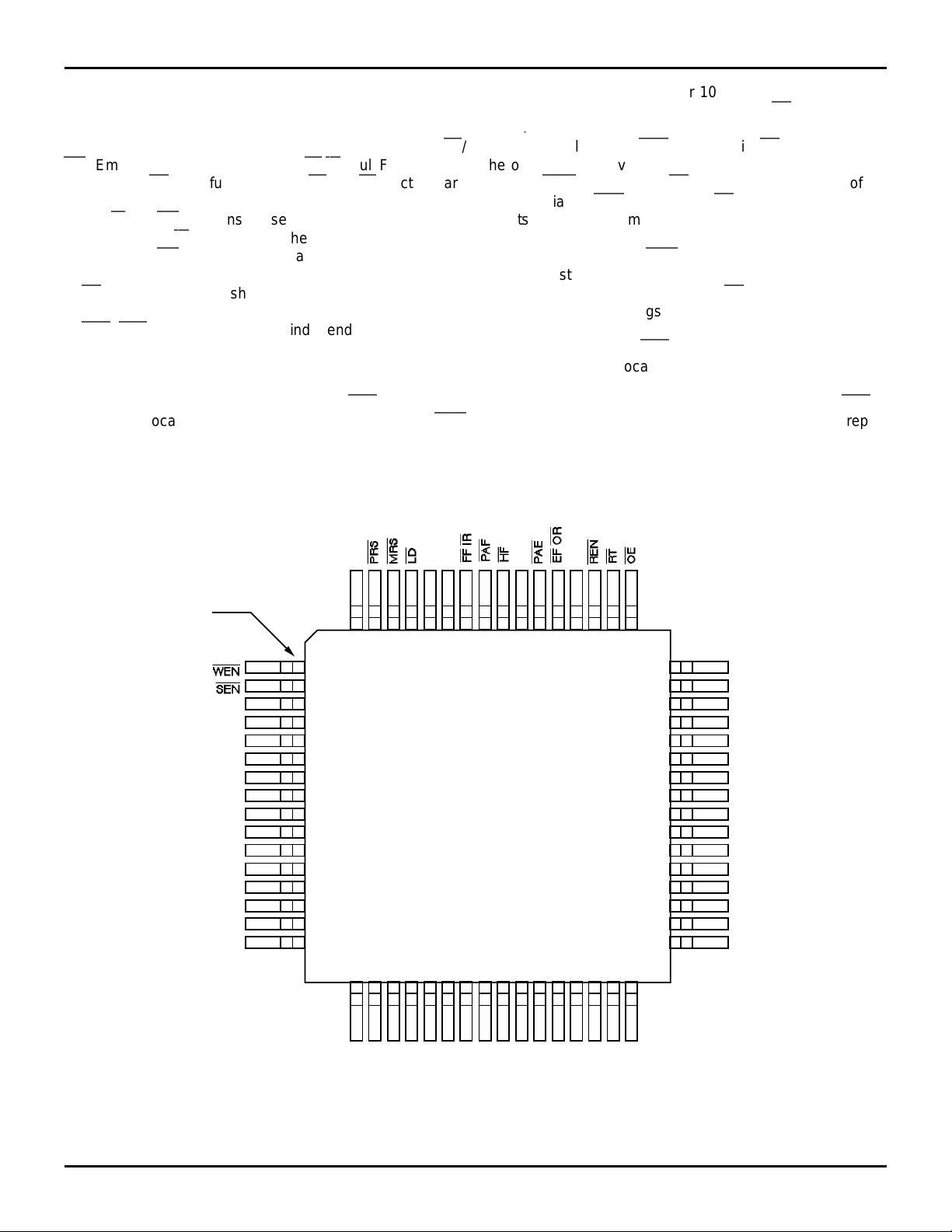
PIN CONFIGURATIONS
threshold can be set at 127 or 1023 locations from the full
boundary. All these choices are made with LD during Master
Reset
.
In the serial method, SEN
together with LD are used to load
the offset registers via the Serial Input (SI). In the parallel
method,
registers via Dn.
WEN
together with LD can be used to load the offset
REN
together with LD can be used to read the
offsets in parallel from Qn regardless of whether serial or
parallel offset loading is selected.
During Master Reset (
MRS
), the read and write pointers are
set to the first location of the FIFO. The FWFT line selects IDT
Standard Mode or FWFT Mode. The LD pin selects one of two
partial flag default settings (127 or 1023) and, also, serial or
parallel programming. The flags are updated accordingly.
The Partial Reset (
PRS
) also sets the read and write
pointers to the first location of the memory. However, the
mode setting, programming method, and partial flag offsets
are not altered. The flags are updated accordingly.
PRS
is
useful for resetting a device in mid-operation, when repro-
PIN 1
FS
V
CC
GND
D17
D16
D15
D14
D13
D12
D11
D10
D9
D8
D7
WCLK
64 63 62 61 60 59 58 57 56 55 54 53 52 51 50 49
1
2
3
4
5
6
7
8
9
10
11
12
13
14
15
16
17 18 19 20 21 22 23 24 25 26 27 28 29 30 31 32
FWFT/SI
GND
/
CC
V
/
RCLK
48
47
46
45
44
43
42
41
40
39
38
37
36
35
34
33
Q17
Q16
GND
Q15
Q14
V
CC
Q13
Q12
Q11
GND
Q10
Q9
Q8
Q7
Q6
GND
D6
D5
D4
D3
D2
D1
D0
GND
Q0
Q1
TQFP (PN64-1, order code: PF)
STQFP (PP64-1, order code: TF)
TOP VIEW
GND
Q2
Q3
CC
V
Q4
Q5
3037 drw 02
2
IDT72255/72265 SyncFIFO
8,192 x 18, 16,384 x 18
MILITARY AND COMMERCIAL TEMPERATURE RANGES
gramming offset registers may not be convenient.
The Retransmit function allows the read pointer to be reset
to the first location in the RAM array. It is synchronized to
RCLK when RT is LOW. This feature is convenient for
sending the same data more than once.
If, at any time, the FIFO is not actively performing a function,
the chip will automatically power down. This occurs if neither
a read nor a write occurs within 10 cycles of the faster clock,
RCLK or WCLK. During the Power Down state, supply current
consumption (ICC2) is at a minimum. Initiating any operation
(by activating control inputs) will immediately take the device
PIN CONFIGURATIONS (CONT.)
11
10
09
Q6
8 Q7
Q
DNC
GND
Q5
CC
V
3Q4 GND
Q
Q2
out of the Power Down state.
The IDT72255/72265 are depth expandable. The addition
of external components is unnecessary. The IR and
functions, together with
total FIFO memory capacity.
The FS line ensures optimal data flow through the FIFO. It
is tied to GND if the RCLK frequency is higher than the WCLK
frequency or to Vcc if the RCLK frequency is lower than the
WCLK frequency
The IDT72255/72265 is fabricated using IDT’s high speed
submicron CMOS technology.
Q1
Q0 D2
D0
D3D1
D
REN
and
WEN
, are used to extend the
D5GND
D9
D7D6
D8
4
OR
LD
D11
D13
D
15
17
D
V
CC
SEN
WCLK
PRS
08
07
06
05
04
03
02
01
Q10
GND
11
Q
Q13 Q12
V
Q14
Q17
Q15
Q16
GND
DNC
Q9
CC
RT
RENOE
RCLK
Pin 1 Designator
GND
EF
OR
/
PAE
VCC
HF
PAF
FF
/
IR
GND
DNC
FWFT/
SI
MRS
ABCDEFGHJ KL
3037 drw 03
PGA (G68-1, order code: G)
TOP VIEW
D10
D12
D14
D16
GND
FS
WEN
NOTES:
1. DNC = Do not connect
3

IDT72255/72265 SyncFIFO
8,192 x 18, 16,384 x 18
MILITARY AND COMMERCIAL TEMPERATURE RANGES
PIN DESCRIPTION
Symbol Name I/O Description
0–D17 Data Inputs I Data inputs for a 18-bit bus.
D
MRS
PRS
RT
FWFT/SI First Word Fall I During Master Reset, selects First Word Fall Through or IDT Standard mode.
WCLK Write Clock I When enabled by
WEN
RCLK Read Clock I When enabled by
REN
OE
SEN
LD
FS Frequency Select I The FS setting optimizes data flow through the FIFO.
FF/IR
EF/OR
PAF
PAE
HF
Q
0–Q17 Data Outputs O Data outputs for a 18-bit bus.
CC Power +5 volt power supply pins.
V
GND Ground Ground pins.
Master Reset I
MRS
initializes the read and write pointers to zero and sets the output register to
all zeroes. During Master Reset, the FIFO is configured for either FWFT or IDT
Standard Mode, one of two programmable flag default settings, and serial or
parallel programming of the offset settings.
Partial Reset I
PRS
initializes the read and write pointers to zero and sets the output register to
all zeroes. During Partial Reset,the existing mode (IDT or FWFT), programming
method (serial or parallel), and programmable flag settings are all retained.
Retransmit I Allows data to be resent starting with the first location of FIFO memory.
Through/Serial In After Master Reset, this pin functions as a serial input for loading offset registers
WEN
, the rising edge of WCLK writes data into the FIFO and
offsets into the programmable registers.
Write Enable I
WEN
enables WCLK for writing data into the FIFO memory and offset registers.
REN
, the rising edge of RCLK reads data from the FIFO
memory and offsets from the programmable registers.
Read Enable I
Output Enable I OE controls the output impedance of Q
Serial Enable I
REN
enables RCLK for reading data from the FIFO memory and offset registers.
n
SEN
enables serial loading of programmable flag offsets
Load I During Master Reset, LD selects one of two partial flag default offsets (127 and
1023) and determines programming method, serial or parallel. After Master
Reset, this pin enables writing to and reading from the offset registers.
Full Flag/ O In the IDT Standard Mode, the FF function is selected. FF indicates whether or
Input Ready not the FIFO memory is full. In the FWFT mode, the IR function is selected.
indicates whether or not there is space available for writing to the FIFO memory.
Empty Flag/ O In the IDT Standard Mode, the EF function is selected.
EF
indicates whether or
Output Ready not the FIFO memory is empty. In FWFT mode, the OR function is selected.
OR
indicates whether or not there is valid data available at the outputs.
Programmable O
Almost Full Flag offset m which is stored in the Full Offset register.
PAF
goes HIGH if the number of free locations in the FIFO memory is more than
PAF
goes LOW if the num-
ber of free locations in the FIFO memory is less than m.
Programmable O
Almost Empty which is stored in theEmpty Offset register.
PAE
goes LOW if the number of words in the FIFO memory is less than offset n
PAE
goes HIGH if the number of
Flag words in the FIFO memory is greater than offset n.
Half-full Flag O
HF
indicates whether the FIFO memory is more or less than half-full.
IR
3037 tbl 01
4
IDT72255/72265 SyncFIFO
8,192 x 18, 16,384 x 18
MILITARY AND COMMERCIAL TEMPERATURE RANGES
ABSOLUTE MAXIMUM RATINGS
(1)
Symbol Rating Commercial Military Unit
V
TERM Terminal Voltage –0.5 to +7.0 –0.5 to +7.0 V
with respect to GND
T
A Operating 0 to +70 –55 to +125 °C
Temperature
T
BIAS Temperature Under –55 to +125 –65 to +135 °C
Bias
STG Storage –55 to +125 –65 to +155 °C
T
Temperature
I
OUT DC Output Current 50 50 mA
NOTE: 3037 tbl 02
1. Stresses greater than those listed under ABSOLUTE MAXIMUM RATINGS may cause permanent damage to the device. This is a stress rating only
and functional operation of the device at these or any other conditions above
those indicated in the operational sections of this specification is not implied.
Exposure to absolute maimum rating conditions for extended periods may
affect reliabilty.
RECOMMENDED DC
OPERATING CONDITIONS
Symbol Parameter Min. Typ. Max. Unit
V
CCM Military Supply 4.5 5.0 5.5 V
Voltage
V
CCC Commercial Supply 4.5 5.0 5.5 V
Voltage
GND Supply Voltage 0 0 0 V
IH Input High Voltage 2.0 — — V
V
Commercial
V
IH Input High Voltage 2.2 — — V
Military
(1)
V
IL
NOTE: 3037 tbl 03
1. 1.5V undershoots are allowed for 10ns once per cycle.
Input Low Voltage — — 0.8 V
Commercial & Military
DC ELECTRICAL CHARACTERISTICS
(Commercial: VCC = 5V ± 10%, TA = 0°C to +70°C; Military: VCC = 5V ± 10%, TA = –55°C to +125°C)
DT72255L IDT72255L
IDT72265L IDT72265L
Commercial Military
CLK = 10, 12,15, 20ns tCLK = 15, 25ns
t
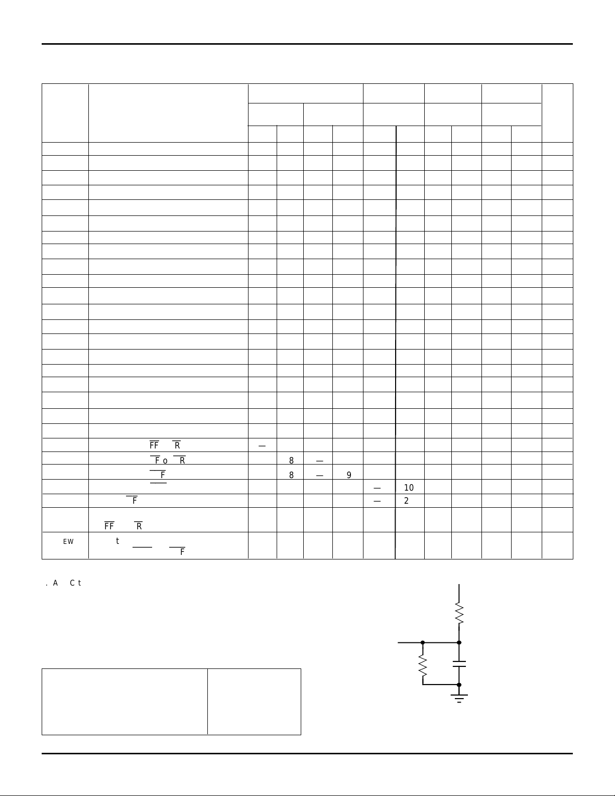
Symbol Parameter Min. Typ. Max. Min. Typ. Max. Unit
(1)
LI
I
I
LO
V
OH Output Logic “1” Voltage, IOH = –2 mA 2.4 — — 2.4 — — V
OL Output Logic “0” Voltage, IOL = 8 mA — — 0.4 — — 0.4 V
V
I
CC1
I
CC2
NOTES:
1. Measurements with 0.4 ≤ VIN ≤ VCC.
2. OE = V
3. Tested at f = 20 MHz with outputs unloaded.
4. No data written or read for more than 10 cycles
Input Leakage Current (any input) –1 — 1 –10 — 10 µA
(2)
Output Leakage Current –10 — 10 –10 — 10 µA
(3)
Active Power Supply Current — — 180 — — 250 mA
(3,4)
Power Down Current (All inputs = VCC - 0.2V or — — 15 — — 25 mA
GND + 0.2V, RCLK and WCLK are free-running)
IH
3037 tbl 04
CAPACITANCE (TA = +25°C, f = 1.0MHz)
Symbol Parameter
(2)
C
IN
Input VIN = 0V 10 pF
Capacitance
(1,2)
C
OUT
Output VOUT = 0V 10 pF
Capacitance
NOTES:
1. With output deselected, (OE=HIGH).
2. Characterized values, not currently tested.
(1)
Conditions Max. Unit
3037 tbl 05
5
IDT72255/72265 SyncFIFO
8,192 x 18, 16,384 x 18
MILITARY AND COMMERCIAL TEMPERATURE RANGES
AC ELECTRICAL CHARACTERISTICS
(1)
(Commercial: VCC = 5V ± 10%, TA = 0°C to +70°C; Military: VCC = 5V ± 10%, TA = –55°C to +125°C)
Commercial Com'l & Mil. Commercial Military
72255L10 72255L12 72255L15 72255L20 72255L25
72265L10 72265L12 72265L15 72265L20 72265L25
Symbol Parameter Min. Max. Min. Max. Min. Max. Min. Max. Min. Max. Unit
f
S Clock Cycle Frequency — 100 — 83.3 — 66.7 — 50 — 40 MHz
A Data Access Time 2 8 2 9 2 10 2 12 3 15 ns
t
CLK Clock Cycle Time 10 — 12 — 15 — 20 — 25 — ns
t
CLKH Clock High Time 4.5 — 5 — 6 — 8 — 10 — ns
t
t
CLKL Clock Low Time 4.5
DS Data Set-up Time 3.5 — 3.5 — 4 — 5 — 6 — ns
t
DH Data Hold Time 0 — 0 — 1 — 1 — 1 — ns
t
t
ENS Enable Set-up Time 3.5 — 3.5 — 4 — 5 — 6 — ns
ENH Enable Hold Time 0 — 0 — 1 — 1 — 1 — ns
t
LDS Load Set-up Time 3.5 — 3.5 — 4 — 5 — 6 — ns
t
t
LDH Load Hold Time 6.5 — 8.5 — 10 — 10 — 10 — ns
FF
EF
PAF
PAE
and
or
or
(3)
(4)
(4)
IR
OR
PAF
RS Reset Pulse Width
t
RSS Reset Set-up Time 10 — 12 — 15 — 20 — 25 — ns
t
t
RSR Reset Recovery Time 10 — 12 — 15 — 20 — 25 — ns
RSF Reset to Flag and Output Time — 10 — 12 — 15 — 20 — 25 ns
t
FWFT Mode Select Time 0 — 0 — 0 — 0 — 0 — ns
t
RTS Retransmit Set-Up Time 3.5 — 3.5 — 4 — 5 — 6 — ns
t
t
OLZ Output Enable to Output in Low Z
OE Output Enable to Output Valid 3 7 3 7.5 3 8 3 10 3 13 ns
t
OHZ Output Enable to Output in High Z
t
t
WFF Write Clock to
REF Read Clock to
t
PAF Write Clock to
t
t
PAE Read Clock to
t
HF Clock to
SKEW1 Skew time between RCLK and WCLK 8 — 10 — 12 — 15 — 20 — ns
t
for FF and
t
SKEW2 Skew time between RCLK and 15 — 18 — 21 — 25 — 35 — ns
WCLK for
NOTES:
1. All AC timings apply to both Standard IDT Mode and First Word Fall
Through Mode.
2. For the RCLK line: t
the programmable flag registers; otherwise, use the table value. For the
WCLK line, use the t
3. Pulse widths less than minimum values are not allowed.
4. Values guaranteed by design, not currently tested.
HF
IR
PAE
CLKL (min.) = 7 ns only when reading the offsets from
CLKL (min.) value given in the table.
(2)
—5
10 — 12 — 15 — 20 — 25 — ns
0—0—0—0 —0 —ns
3 7 3 7.5 3 8 3 10 3 13 ns
—8—9—10—12—15ns
—8—9—10—12—15ns
– 8—9—10—12—15ns
—8—9—10—12—15ns
— 16 — 18 — 20 — 22 — 25 ns
(2)
—6
(2)
D.U.T.
—8 —10—ns
3037 tbl 06
5V
1.1K
AC TEST CONDITIONS
Input Pulse Levels
Input Rise/Fall Times
Input Timing Reference Levels
Output Reference Levels
Output Load
GND to 3.0V
3ns
1.5V
1.5V
See Figure 1
3037 tbl 08
680Ω
Figure 1. Output Load
* Includes jig and scope capacitances.
30pF*
3037 drw 04
6

IDT72255/72265 SyncFIFO
8,192 x 18, 16,384 x 18
MILITARY AND COMMERCIAL TEMPERATURE RANGES
SIGNAL DESCRIPTIONS:
INPUTS:
DATA IN (D
Data inputs for 18-bit wide data.
CONTROLS:
MASTER RESET (
A Master Reset is accomplished whenever the Master
Reset (
the internal read and write pointers to the first location of the
RAM array.
go HIGH.
If FWFT is LOW during Master Reset then the IDT Standard
Mode, along with EF and FF are selected. EF will go LOW and
FF
will go HIGH. If FWFT is HIGH, then the First Word Fall
through Mode (FWFT), along with IR and OR, are selected.
OR
will go HIGH and IR will go LOW.
If LD is LOW during Master Reset, then
threshold 127 words from the empty boundary and
assigned a threshold 127 words from the full boundary; 127
words corresponds to an offset value of 07FH. Following
Master Reset, parallel loading of the offsets is permitted, but
not serial loading.
If LD is HIGH during Master Reset, then
threshold 1023 words from the empty boundary and
assigned a threshold 1023 words from the full boundary;
1023 words corresponds to an offset value of 3FFH. Following
Master Reset, serial loading of the offsets is permitted, but not
parallel loading.
Regardless of whether serial or parallel offset loading has
been selected, parallel reading of the registers is always
permitted. (See section describing the LD line for further
details).
During a Master Reset, the output register is initialized to
all zeroes. A Master Reset is required after power up, before
a write operation can take place.
PARTIAL RESET (
A Partial Reset is accomplished whenever the Partial
Reset (
the Master Reset, the internal read and write pointers are set
to the first location of the RAM array,
goes HIGH, and HF goes HIGH.
Whichever mode is active at the time of partial reset, IDT
Standard Mode or First Word Fall-through, that mode will
remain selected. If the IDT Standard Mode is active, then
will go HIGH and EF will go LOW. If the First word Fall-through
Mode is active, then OR will go HIGH, and IR will go LOW.
Following Partial Reset, all values held in the offset registers remain unchanged. The programming method (parallel
or serial) currently active at the time of Partial Reset is also
retained. The output register is initialized to all zeroes.
is asynchronous.
0 - D17)
MRS
)
MRS
MRS
) input is taken to a LOW state. This operation sets
PAE
will go LOW,
PRS
)
PRS
PRS
) input is taken to a LOW state. As in the case of
PAF
will go HIGH, and HF will
PAE
is assigned a
PAE
is assigned a
MRS
is asynchronous.
PAE
goes LOW,
PAF
PAF
is
is
PAF
FF
PRS
A Partial Reset is useful for resetting the device during the
course of operation, when reprogramming flag settings may
not be convenient.
RETRANSMIT (
RTRT)
The Retransmit operation allows data that has already
been read to be accessed again. There are two stages: first,
a setup procedure that resets the read pointer to the first
location of memory, then the actual retransmit, which consists
of reading out the memory contents, starting at the beginning
of memory.
Retransmit Setup is initiated by holding RT LOW during a
rising RCLK edge.
REN
and
WEN
must be HIGH before
bringing RT LOW. At least one word, but no more than Full 2 words should have been written into the FIFO between
Reset (Master or Partial) and the time of Retransmit Setup
(Full = 8,192 words for the 72255, 16,384 words for the
72265).
If IDT Standard mode is selected, the FIFO will mark the
beginning of the Retransmit Setup by setting EF LOW. The
change in level will only be noticeable if EF was HIGH before
setup. During this period, the internal read pointer is initialized
to the first location of the RAM array.
When
EF
goes HIGH, Retransmit Setup is complete and
read operations may begin starting with the first location in
memory. Since IDT Standard Mode is selected, every word
read including the first word following Retransmit Setup requires a LOW on
REN
to enable the rising edge of RCLK.
Writing operations can begin after one of two conditions have
been met: EF is HIGH or 14 cycles of the faster clock (RCLK
or WCLK) have elapsed since the RCLK rising edge enabled
by the RT pulse.
The deassertion time of EF during Retransmit Setup is
variable. The parameter t
RTF1, which is measured from the
rising RCLK edge enabled by RT to the rising edge of EF is
described by the following equation:
tRTF1 max. = 14*Tf + 3*TRCLK (in ns)
where Tf is either the RCLK or the WCLK period, whichever is
shorter, and TRCLK is the RCLK period.
Regarding FF: Note that since no more than Full - 2 writes
are allowed between a Reset and a Retransmit Setup, FF will
remain HIGH throughout the setup procedure.
For IDT Standard mode, updating the
flags begins with the "first"
REN
-enabled rising RCLK edge
following the end of Retransmit Setup (the point at which
PAE, HF
, and
PAF
EF
goes HIGH). This same RCLK rising edge is used to access
the "first" memory location. HF is updated on the first RCLK
rising edge.
edges.
followed by the next two rising WCLK edges. (If the t
PAE
is updated after two more rising RCLK
PAF
is updated after the "first" rising RCLK edge,
skew2
specification is not met, add one more WCLK cycle.)
If FWFT mode is selected, the FIFO will mark the beginning
of the Retransmit Setup by setting OR HIGH. The change in
level will only be noticeable if OR was LOW before setup.
During this period, the internal read pointer is set to the first
location of the RAM array.
7

IDT72255/72265 SyncFIFO
8,192 x 18, 16,384 x 18
MILITARY AND COMMERCIAL TEMPERATURE RANGES
When
OR
goes LOW, Retransmit Setup is complete; at the
same time, the contents of the first location are automatically
displayed on the outputs. Since FWFT Mode is selected, the
first word appears on the outputs, no read request necessary.
Reading all subsequent words requires a LOW on
REN
to
enable the rising edge of RCLK. Writing operations can begin
after one of two conditions have been met: OR is LOW or 14
cycles of the faster clock (RCLK or WCLK) have elapsed since
the RCLK rising edge enabled by the RT pulse.
The assertion time of OR during Retransmit Setup is
variable. The parameter tRTF2, which is measured from the
rising RCLK edge enabled by RT to the falling edge of OR is
described by the following equation:
tRTF2 max. = 14*Tf + 4*TRCLK (in ns)
where Tf is either the RCLK or the WCLK period, whichever
is shorter, and TRCLK is the RCLK period. Note that a
Retransmit Setup in FWFT mode requires one more RCLK
cycle than in IDT Standard mode.
Regarding IR: Note that since no more than Full - 2 writes
are allowed between a Reset and a Retransmit Setup, IR will
remain LOW throughout the setup procedure.
For FWFT mode, updating the
PAE, HF
, and
PAF
flags
begins with the "last" rising edge of RCLK before the end of
Retransmit Setup. This is the same edge that asserts OR and
automatically accesses the first memory location. Note that,
in this case,
is updated on the "last" RCLK rising edge.
after two more rising RCLK edges.
REN
is not required to initiate flag updating.
PAE
PAF
is updated after the
HF
is updated
"last" rising RCLK edge, followed by the next two rising WCLK
edges. (If the t
skew2 specification is not met, add one more
WCLK cycle.)
RT
is synchronized to RCLK. The Retransmit operation is
useful in the event of a transmission error on a network, since
it allows a data packet to be resent.
FIRST WORD FALL THROUGH/SERIAL IN (FWFT/SI)
This is a dual purpose pin. During Master Reset, the state
of the FWFT/SI helps determine whether the device will
operate in IDT Standard mode or First Word Fall Through
(FWFT) mode.
If, at the time of Master Reset, FWFT/SI is LOW, then IDT
Standard mode will be selected. This mode uses the Empty
Flag (EF) to indicate whether or not there are any words
present in the FIFO memory. It also uses the Full Flag function
(FF) to indicate whether or not the FIFO memory has any free
space for writing. In IDT Standard mode, every word read
from the FIFO, including the first, must be requested using the
Read Enable (
REN
) line.
If, at the time of Master Reset, FWFT/SI is HIGH, then
FWFT mode will be selected. This mode uses Output Ready
(OR) to indicate whether or not there is valid data at the data
outputs (Q
n). It also uses Input Ready (
IR
) to indicate whether
or not the FIFO memory has any free space for writing. In the
FWFT mode, the first word written to an empty FIFO goes
directly to Qn, no read request necessary. Subsequent words
must be accessed using the Read Enable (
REN
) line.
After Master Reset, FWFT/SI acts as a serial input for
loading
PAE
and
PAF
offsets into the programmable registers.
The serial input function can only be used when the serial
loading method has been selected during Master Reset.
FWFT/SI functions the same way in both IDT Standard and
FWFT modes.
WRITE CLOCK (WCLK)
A write cycle is initiated on the rising edge of the write clock
(WCLK). Data set-up and hold times must be met with respect
to the LOW-to-HIGH transition of the WCLK. The write and
read clocks can either be asynchronous or coincident.
WRITE ENABLE (
When Write Enable (
WEN
WEN
)
WEN
) is LOW, data can be loaded into
the input register on the rising edge of every WCLK cycle.
Data is stored in the RAM array sequentially and independently of any on-going read operation.
When
WEN
is HIGH, the input register holds the previous
data and no new data is loaded into the FIFO.
To prevent data overflow in the IDT Standard Mode, FF will
go LOW , inhibiting further write operations. Upon the completion of a valid read cycle, FF will go HIGH allowing a write to
occur.
WEN
is ignored when the FIFO is full.
To prevent data overflow in the FWFT mode, IR will go
HIGH, inhibiting further write operations. Upon the completion
of a valid read cycle, IR will go LOW allowing a write to occur.
WEN
is ignored when the FIFO is full.
READ CLOCK (RCLK)
Data can be read on the outputs, on the rising edge of the
read clock (RCLK), when Output Enable (OE) is set LOW. The
write and read clocks can be asynchronous or coincident.
READ ENABLE (
When Read Enable (
REN
REN
)
REN
) is LOW, data is loaded from the
RAM array into the output register on the rising edge of the
RCLK.
When
REN
is HIGH, the output register holds the previous
data and no new data is loaded into the output register.
In the IDT Standard Mode, every word accessed at Q
including the first word written to an empty FIFO, must be
requested using
REN
. When all the data has been read from
the FIFO, the Empty Flag (EF) will go LOW, inhibiting further
read operations.
REN
is ignored when the FIFO is empty.
Once a write is performed, EF will go HIGH after tFWL1 +tREF
and a read is permitted.
In the FWFT Mode, the first word written to an empty FIFO
automatically goes to the outputs Qn, no need for any read
request. In order to access all other words, a read must be
executed using
REN
. When all the data has been read from
the FIFO, Output Ready (OR) will go HIGH, inhibiting further
read operations.
REN
is ignored when the FIFO is empty.
Once a write is performed, OR will go LOW after tFWL2 +tREF,
when the first word appears at Qn ; if a second word is written
into the FIFO, then
REN
can be used to read it out.
n,
8
IDT72255/72265 SyncFIFO
8,192 x 18, 16,384 x 18
MILITARY AND COMMERCIAL TEMPERATURE RANGES
SERIAL ENABLE (
Serial Enable is (
SEN
)
SEN
SEN
) is an enable used only for serial
programming of the offset registers. The serial programming
method must be selected during Master Reset.
SEN
is always
used in conjunction with LD. When these lines are both LOW,
data at the SI input can be loaded into the input register one
bit for each LOW-to-HIGH transition of WCLK.
When
SEN
is HIGH, the programmable registers retains
the previous settings and no offsets are loaded.
SEN
functions the same way in both IDT Standard and
FWFT modes.
OUTPUT ENABLE (
OEOE)
When Output Enable (OE) is enabled (LOW), the parallel
output buffers receive data from the output register. When
OE
is HIGH, the output data bus (Qn) goes into a high impedance
state.
LOAD (
LDLD)
This is a dual purpose pin. During Master Reset, the state
of the Load line (LD) determines one of two default values (127
or 1023) for the
PAE
and
PAF
flags, along with the method by
which these flags can be programmed, parallel or serial. After
Master Reset, LD enables write operations to and read
operations from the registers. Only the offset loading method
currently selected can be used to write to the registers. Aside
from Master Reset, there is no other way change the loading
method. Registers can be read only in parallel; this can be
accomplished regardless of whether serial or the parallel
loading has been selected.
Associated with each of the programmable flags,
PAF
, are registers which can either be written to or read from.
PAE
and
Offset values contained in these registers determine how
many words need to be in the FIFO memory to switch a partial
flag. A LOW on LD during Master Reset selects a default
PAE
offset value of 07FH ( a threshold 127 words from the empty
boundary), a default
PAF
offset value of 07FH (a threshold 127
words from the full boundary), and parallel loading of other
offset values. A HIGH on LD during Master Reset selects a
default
the empty boundary), a default
PAE
offset value of 3FFH (a threshold 1023 words from
PAF
offset value of 3FFH (a
threshold 1023 words form the full boundary), and serial
loading of other offset values.
The act of writing offsets (in parallel or serial) employs a
dedicated write offset register pointer. The act of reading
offsets employs a dedicated read offset register pointer. The
WCLK
0
0
0
X
1
1
1
0
1
1
1
0
X
1
1
0
1
1
X
0
1
1
1
0
1
X
X
X
X
X
X
X
RCLK
X
X
X
X
X
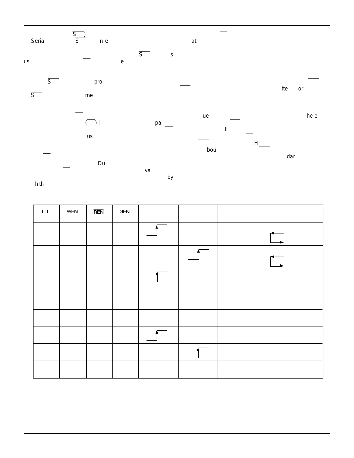
Parallel write to registers:
Empty Offset
Full Offset
Parallel read from registers:
Empty Offset
Full Offset
Serial shift into registers:
26 bits for the 72255
28 bits for the 72265
1 bit for each rising WCLK edge
Starting with Empty Offset (LSB)
Ending with Full Offset (MSB)
No Operation
Write Memory
Read Memory
No Operation
Selection
NOTES:
1. Only one of the two offset programming methods, serial or parallel, is available for use at any given time.
2. The programming method can only be selected at Master Reset.
3. Parallel reading of the offset registers is always permitted regardless of which programming method has been selected.
4. The programming sequence applies to both IDT Standard and FWFT modes.
Figure 2. Partial Flag Programming Sequence
3037 tbl 02
9

IDT72255/72265 SyncFIFO
8,192 x 18, 16,384 x 18
MILITARY AND COMMERCIAL TEMPERATURE RANGES
two pointers operate independently; however, a read and a
write should not be performed simultaneously to the offset
registers. A Master Reset initializes both pointers to the
Empty Offset (LSB) register. A Partial Reset has no effect on
the position of these pointers.
Once serial offset loading has been selected, then pro-
gramming
SEN
PAE
and
PAF
procedes as follows: When LD and
are set LOW, data on the SI input are written, one bit for
each WCLK rising edge, starting with the Empty Offset (13 bits
for the 72255, 14 bits for the 72265), ending with the Full Offset
(13 bits for the 72255, 14 bits for the 72265). A total of 26 bits
are necessary to program the 72255; a total of 28 bits are
necessary to program the 72265. Individual registers cannot
be loaded serially; rather, both must be programmed in
sequence, no padding allowed.
PAE
and
PAF
can show a
valid status only after the the full set of bits have been entered.
The registers can be re-programmed, as long as both offsets
are loaded. When LD is LOW and
SEN
is HIGH, no serial write
to the registers can occur.
Once parallel offset loading has been selected, then
programming
and
WEN
PAE
and
PAF
procedes as follows: When
are set LOW, data on the inputs D
LD
n are written into
the Empty Offset Register on the first LOW-to-HIGH transition
of WCLK. Upon the second LOW-to-HIGH transition of
WCLK, data at the inputs are written into the Full Register. The
third transition of WCLK writes, once again, to the Empty
Offset Register.
To ensure proper programming (serial or parallel) of the
offset registers, no read operation is permitted from the time
of reset (master or partial) to the time of programming. (During
this period, the read pointer must be pointing to the first
location of the memory array.) After the programming has
been accomplished, read operations may begin.
Write operations to memory are allowed before and during
the parallel programming sequence. In this case, the programming of all offset registers does not have to occur at one
time. One or two offset registers can be written to and then,
by bringing LD HIGH, write operations can be redirected to the
FIFO memory. When LD is set LOW again, and
WEN
is LOW,
the next offset register in sequence is written to. As an
alternative to holding
WEN
LOW and toggling LD, parallel
programming can also be interrupted by setting LD LOW and
toggling
WEN
.
Write operations to memory are allowed before and during
the serial programming sequence. In this case, the programming of all offset bits does not have to occur at once. A select
number of bits can be written to the SI input and then, by
bringing LD and
memory via D
with LD and
SEN
HIGH, data can be written to FIFO
n by toggling
SEN
restored to a LOW, the next offset bit in
WEN
. When
WEN
is brought HIGH
sequence is written to the registers via SI. If a mere interuption
of serial programming is desired, it is sufficient either to set
LOW and deactivate
LD
. Once LD and
SEN
or to set
SEN
are both restored to a LOW level, serial
SEN
LOW and deactivate
LD
offset programming continues from where it left off.
Note that the status of a partial flag (
PAE
or
PAF
) output is
invalid during the programming process. From the time
parallel programming has begun, a partial flag output will not
be valid until the appropriate offset word has been written to
the register pertaining to that flag. From the time serial
programming has begun, neither partial flag will be valid until
the full set of bits required to fill all the offset registers has been
written. Measuring from the rising WCLK edge that achieves
either of the above criteria;
rising WCLK edges plus t
PAF
will be valid after two more
PAF,
PAE
will will be valid after the
next two rising RCLK edges plus tPAE (Add one more RCLK
cycle if tSKEW2 is not met.)
The act of reading the offset registers employs a dedicated
read offset register pointer. The contents of the offset registers
can be read on the output lines when LD is set LOW and
REN
is set LOW; then, data are read via Qn from the Empty Offset
Register on the first LOW-to-HIGH transition of RCLK. Upon
the second LOW-to-HIGH transition of RCLK, data are read
from the Full Offset Register. The third transition of RCLK,
reads, once again, from the Empty Offset Register.
It is permissable to interrupt the the offset register access
sequence with reads or writes to memory . The interruption is
accomplished by deasserting
When
REN
and LD are restored to a LOW level, access of the
REN, LD
, or both together.
registers continues where it left off.
LD
functions the same way in both IDT Standard and
FWFT modes.
FREQUENCY SELECT INPUT (FS)
An internal state machine manages the movement of data
through the SuperSync FIFO. The FS line determines whether
RCLK or WCLK will synchronize the state machine. Tie FS to
V
CC if the RCLK line is running at a lower frequency than the
WCLK line. In this case, the state machine will be synchronized to WCLK. Tie FS to GND if the RCLK line is running at
a higher frequency than the WCLK line. In this case, the state
machine will be synchronized to RCLK. Note that FS must be
set so the clock line running at the higher frequency drives the
state machine; this ensures efficient handling of the data
within the FIFO. If the same clock signal drives both the WCLK
and the RCLK pins, then tie FS to GND.
The frequency of the clock tied to the state machine
(referred to as the "selected clock") may be changed at any
time, so long as it is always greater than or equal to the
frequency of the clock that is not tied to the state machine
(referred to as the "non-selected clock"). The frequency of the
non-selected clock can also be varied with time, so long as it
never exceeds the frequency of the selected clock. To be
more specific, the frequencies of both RCLK and WCLK may
be varied during FIFO operation, provided that, at any given
point in time, the cycle period of the selected clock is equal to
or less than the cycle period of the non-selected clock.
The selected clock must be continuous. It is, however,
permissible to stop the non-selected clock. Note, so long as
RCLK is idle, EF/OR and
as long as WCLK is idle, FF/IR and
PAE
will not be updated. Likewise,
PAF
will not be updated.
Changing the FS setting during FIFO operation (i.e. reading or writing) is not permitted; however, such a change at the
time of Master Reset or Partial Reset is all right. FS is an
asynchronous input.
10

IDT72255/72265 SyncFIFO
8,192 x 18, 16,384 x 18
OUTPUTS:
FULL FLAG (
FFFF/
IRIR)
This is a dual purpose pin. In IDT Standard Mode, the Full
Flag (FF) function is selected. When the FIFO is full (i.e. the
write pointer catches up to the read pointer), FF will go LOW,
inhibiting further write operation. When FF is HIGH, the FIFO
is not full. If no reads are performed after a reset (either MRS
or PRS), FF will go LOW after 8,192 writes tor the IDT72255
and 16,384 writes to the IDT72265.
In FWFT Mode, the Input Ready (IR) function is selected.
IR goes LOW when memory space is available for writing in
data. When there is no longer any free space left, IR goes
HIGH, inhibiting further write operation. If no reads are
performed after a reset (either MRS or PRS), IR will go HIGH
after 8,193 writes for the IDT72255 and 16,385 writes for the
IDT72265.
The IR status not only measures the contents of the FIFO
memory, but also counts the presence of a word in the output
register. Thus, in FWFT mode, the total number of writes
necessary to deassert IR is one greater than needed to assert
FF in IDT Standard mode.
FF/IR is synchronized to WCLK. It is double-registered to
enhance metastable immunity.
EMPTY FLAG (
EFEF/
OROR)
This is a dual purpose pin. In the IDT Standard Mode, the
Empty Flag (EF) function is selected. When the FIFO is empty
(i.e. the read pointer catches up to the write pointer), EF will go
LOW, inhibiting further read operations. When EF is HIGH, the
FIFO is not empty.
When writing the first word to an empty FIFO, the deassertion
time of EF is variable, and can be represent by the First Word
Latency parameter, t
FWL1, which is measured from the rising
WCLK edge that writes the first word to the rising RCLK edge
MILITARY AND COMMERCIAL TEMPERATURE RANGES
that updates the flag. tFWL1 includes any delays due to clock
skew and can be expressed as follows:
tFWL1 max. = 10*Tf + 2*TRCLK (in ns)
where Tf is either the RCLK or the WCLK period, whichever is
shorter, and TRCLK is the RCLK period. Since no read can
take place until EF goes HIGH, the tFWL1 delay determines
how early the first word can be available at Qn. This delay has
no effect on the reading of subsequent words.
In FWFT Mode, the Ouput Ready (OR) function is selected.
OR
goes LOW at the same time that the first word written to an
empty FIFO appears valid on the outputs. OR goes HIGH one
cycle after RCLK shifts the last word from the FIFO memory
to the outputs. Then further data reads are inhibited until
OR
goes LOW again.
When writing the first word to an empty FIFO, the assertion
time of OR is variable, and can be represented by the First
Word Latency parameter, t
FWL2, which is measured from the
rising WCLK edge that writes the first word to the rising RCLK
edge that updates the flag. tFWL2 includes any delay due to
clock skew and can be expressed as follows:
tFWL2 max. = 10*Tf + 3*TRCLK (in ns)
where Tf is either the RCLK or the WCLK period, whichever is
shorter, and TRCLK is the RCLK period. Note that the First
Word Latency in FWFT mode is one RCLK cycle longer than
in IDT Standard mode. The tFWL2 delay determines how early
the first word can be available at Qn. This delay has no effect
on the reading of subsequent words.
EF/OR is sychronized to the RCLK. It is double-registered
to enhance metastable immunity.
72255 – 8,192 x 18–BIT
17 0
17 0
NOTE:
1. Any bits of the offset register not being programmed should be set to zero.
12
EMPTY OFFSET REGISTER
DEFAULT VALUE
07FH if LD is LOW at Master Reset,
3FFH if LD is HIGH at Master Reset
12
FULL OFFSET REGISTER
DEFAULT VALUE
07FH if LD is LOW at Master Reset,
3FFH if LD is HIGH at Master Reset
3037 drw 05
Figure 3. Offset Register Location and Default Values
72265 – 16,384 x 18–BIT
17 0
17 0
13
EMPTY OFFSET REGISTER
DEFAULT VALUE
07FH if LD is LOW at Master Reset,
3FFH if LD is HIGH at Master Reset
13
FULL OFFSET REGISTER
DEFAULT VALUE
07FH if LD is LOW at Master Reset,
3FFH if LD is HIGH at Master Reset
3037 drw 06
11

IDT72255/72265 SyncFIFO
8,192 x 18, 16,384 x 18
MILITARY AND COMMERCIAL TEMPERATURE RANGES
PROGRAMMABLE ALMOST-FULL FLAG (
The Programmable Almost-Full Flag (
when the FIFO reaches the Almost-Full condition as specified
by the offset m stored in the Full Offset register.
At the time of Master Reset, depending on the state of LD,
one of two possible default offset values are chosen. If LD is
LOW, then m = 07FH and the
PAF
switching threshold is 127
words from the Full boundary, if LD is HIGH, then m = 3FFH
and the
PAF
switching threshold is 1023 words away from the
Full boundary.
Any integral value of m from 0 to the maximum FIFO depth
minus 1 (8,191 words for the 72255, 16,383 words for the
72265) can be programmed into the Full Offset register.
In IDT Standard Mode, if no reads are performed after reset
(
MRS
or
PRS
),
PAF
will go LOW after (8,192-m) writes to the
PAF
)
PAF
PAF
) will go LOW
IDT72255, and (16,384-m) writes to the IDT72265.
In FWFT Mode, if no reads are performed after reset (
or
PRS
),
PAF
will go LOW after (8,193-m) writes to the
IDT72255, and (16,385-m) writes to the IDT72265. In this
case, the first word written to an empty FIFO does not stay in
memory, but goes unrequested to the output register; therefore, it has no effect on determining the state of
Note that even though
during the first word latency period (t
PAF
is programmed to switch LOW
FWL), attempts to read
data will be ignored until EF goes HIGH indicating that data is
available at the output port. This is true for both timing modes.
PAF
is synchronous and updated on the rising edge of
WCLK. It is double-registered to enhance metastable immunity.
TABLE I –– STATUS FLAGS FOR IDT STANDARD MODE
Number of Words in FIFO Memory
72255
0
(2)
1 to n
(n+1) to 4,096
4,097 to (8192-(m+1))
(8,192-m) to 8,191
NOTES:
1. Data in the output register does not count as a 'word in FIFO memory". Since in FWFT mode, the first word written to an empty FIFO goes
unrequested to the output register (no read operation necessary), it is not included in the FIFO memory count.
2. n = Empty Offset, Default Values: n = 127 when parallel offset loading is selected or n=1023 when serial offset loading is selected.
3. m = Full Offset, Default Values: m = 127 when parallel offset loading is selected or n=1023 when serial offset loading is selected.
(3)
8,192
8,193 to (16,384-(m+1))
(16,384-m) to 16,383
(1)
72265
0
(2)
1 to n
(n+1) to 8,192
(3)
16,384
FF
FF
H
H
H
H
H
L
PAF
PAF
HH
HH
HH
HL
LL
LL
HF
HF
PAE
PAE
L
L
H
H
H
H
PAF
3037 tbl 03
MRS
.
EF
EF
L
H
H
H
H
H
TABLE II –– STATUS FLAGS FOR FWFT MODE
Number of Words in FIFO Memory
72255
0L
(2)
1 to n L
(n+1) to 4,096 L
4,097 to (8192-(m+1)) L
(8,192-m) to 8,191 L
(3)
8,193 to (16,384-(m+1))
(16,384-m) to 16,383
8,192 H
NOTES:
1.Data in the output register does not count as a 'word in FIFO memory". Since in FWFT mode, the first word written to an empty FIFO
goes unrequested to the output register (no read operation necessary), it is not included in the FIFO memory count.
2. n = Empty Offset, Default Values: n = 127 when parallel offset loading is selected or n=1023 when serial offset loading is selected.
3. m = Full Offset, Default Values: m = 127 when parallel offset loading is selected or n=1023 when serial offset loading is selected.
4. Following a reset (Master or Partial), the FIFO memory is empty and OR = HIGH. After writing the first word, the FIFO memory remains empty,
the data is placed into the output register, and OR goes LOW. In this case, or any time the last word in the FIFO memory has been read into the
output register; a rising RCLK edge, enabled by
REN
, will set OR HIGH.
(1)
72265
0
(2)
1 to n
(n+1) to 8,192
(3)
16,384
IR
IR
PAF
PAF
H
H
H
H
L
L
HF
HF
PAE
PAE
HLH
HLL
HHL
LHL
LHL
LHL
3037 tbl 04
OR
OR
(4)
12

IDT72255/72265 SyncFIFO
8,192 x 18, 16,384 x 18
MILITARY AND COMMERCIAL TEMPERATURE RANGES
PROGRAMMABLE ALMOST-EMPTY FLAG (
The Programmable Almost-Empty Flag (
PAE
PAE
PAE
) will go LOW
)
when the FIFO reaches the Almost-Empty condition as specified by the offset n stored in the Empty Offset register.
At the time of Master Reset, depending on the state of LD,
one of two possible default offset values are chosen. If LD is
LOW, then n = 07FH and the
PAE
switching threshold is 127
words from the Empty boundary, if LD is HIGH, then n = 3FFH
and the
PAE
switching threshold is 1023 words away from the
Empty boundary.
Any integral value of n from 0 to the maximum FIFO depth
minus 1 (8,191 words for the 72255, 16,383 words for the
72265) can be programmed into the Empty Offset register.
In IDT Standard Mode, if no reads are performed after
reset (
MRS
or
PRS
), the
PAE
will go HIGH after (n + 1) writes
to the IDT72255/72265.
In FWFT Mode, if no reads are performed after reset (
or
PRS
), the
PAE
will go HIGH after (n+2) writes to the
MRS
IDT72255/72265. In this case, the first word written to an
empty FIFO does not stay in memory, but goes unrequested
to the output register; therefore, it has no effect on determining the state of
Note that even though
during the first word latency period (t
PAE
.
PAE
is programmed to switch HIGH
FWL), attempts to read
data will be ignored until EF goes HIGH indicating that data is
available at the output port. This is true for both timing modes.
PAE
is synchronous and updated on the rising edge of
RCLK. It is double-registered to enhance metastable immunity.
HALF-FULL FLAG (
HFHF)
This output indicates a half-full memory. The rising WCLK
edge that fills the memory beyond half-full sets HF LOW. The
flag remains LOW until the difference between the write and
read pointers becomes less than or equal to half of the total
depth of the device; the rising RCLK edge that accomplishes
this condition also sets HF HIGH.
In IDT Standard Mode, if no reads are performed after reset
(
MRS
or
PRS
), HF will go LOW after (D/2 + 1) writes, where D
is the maximum FIFO depth (8,192 words for the IDT72255,
16,384 words for the IDT72265).
In FWFT Mode, if no reads are performed after reset (
or
PRS
), HF will go LOW after (D/2+2) writes to the IDT72255/
MRS
72265. In this case, the first word written to an empty FIFO
does not stay in memory, but goes unrequested to the output
register; therefore, it has no effect on determining the state of
HF
.
Because HF uses both RCLK and WCLK for synchroniza-
tion purposes, it is asynchronous.
DATA OUTPUTS (Q0-Q17)
Q0-Q17 are data outputs for 18-bit wide data.
13

IDT72255/72265 SyncFIFO
8,192 x 18, 16,384 x 18
MRS
MILITARY AND COMMERCIAL TEMPERATURE RANGES
tRS
REN
WEN
FWFT/SI
LD
RT
SEN
EF/OR
tRSS
tRSS
tFWFT
tRSR
tRSR
tRSR
tRSRtRSS
(1)
tRSS
tRSS
tRSF
If FWFT = HIGH, OR = HIGH
If FWFT = LOW, EF = LOW
FF/IR
PAE
PAF, HF
Q0 - Q17
tRSF
tRSF
tRSF
tRSF
Figure 4. Master Reset Timing
If FWFT = LOW, FF = HIGH
If FWFT = HIGH,
IR
OE
= HIGH
OE
= LOW
= LOW
(1)
3037 drw 07
14

IDT72255/72265 SyncFIFO
8,192 x 18, 16,384 x 18
PRS
MILITARY AND COMMERCIAL TEMPERATURE RANGES
tRS
REN
WEN
RT
SEN
EF/OR
FF/IR
PAE
tRSF
tRSF
tRSF
tRSS
tRSS
tRSS
tRSS
tRSR
tRSR
If FWFT = HIGH, OR = HIGH
If FWFT = LOW, EF = LOW
If FWFT = LOW, FF = HIGH
If FWFT = HIGH,
IR
= LOW
PAF, HF
Q0 - Q17
tRSF
tRSF
Figure 5. Partial Reset Timing
OE
= HIGH
OE
= LOW
(1)
3037 drw 08
15

IDT72255/72265 SyncFIFO
8,192 x 18, 16,384 x 18
WCLK
D
0 - D17
WEN
FF
RCLK
REN
tCLK
tCLKH tCLKL
1
(1)
tSKEW1
MILITARY AND COMMERCIAL TEMPERATURE RANGES
2
tDS
DATAIN VALID
tENS
tWFF tWFF
tDH
tENH
NO OPERATION
3037 drw 09
NOTES:
1. t
SKEW1 is the minimum time between a rising RCLK edge and a rising WCLK edge to guarantee that
If the time between the rising edge of RCLK and the rising edge of WCLK is less than t
SKEW1, then the
cycle.
2. LD = HIGH
Figure 6. Write Cycle Timing (IDT Standard Mode)
FF
will go HIGH (after one WCLK cycle plus tWFF).
FF
deassertion may be delayed an extra WCLK
16

IDT72255/72265 SyncFIFO
8,192 x 18, 16,384 x 18
RCLK
tENS
MILITARY AND COMMERCIAL TEMPERATURE RANGES
tCLK
tCLKH tCLKL
tENH
REN
EF
Q0 - Q17
OE
WCLK
WEN
tREF
tA
tOLZ
tOE
NO OPERATION
tFWL1
tENS
tDS
tREF
LAST WORD
tOHZ
(1)
tENH
tDHS
D0 - D17
NOTES:
1. t
FWL1 contributes a variable delay to the overall first word latency (this parameter includes delays due to skew):
t
FWL1 max. (in ns) = 10*Tf + 2* TRCLK
where Tf is either the RCLK or the WCLK period, whichever is shorter, and TRCLK is the RCLK period
2. LD = HIGH
Figure 7. Read Cycle Timing (IDT Standard Mode)
FIRST WORD
3037 drw 10
17

IDT72255/72265 SyncFIFO
8,192 x 18, 16,384 x 18
WCLK
DS
t
0 - D17
D
WEN
RCLK
EF
REN
D0
first valid write
tENS
MILITARY AND COMMERCIAL TEMPERATURE RANGES
D1
(1)
tFWL1
tREF
Q
0 - Q17
tOLZ
OE
tOE
NOTES:
FWL1 max. (in ns) = 10* Tf + 2* TRCLK
1. t
Where Tf is either the RCLK or the WCLK period, whichever is shorter, and TRCLK is the RCLK period
2. LD = HIGH
Figure 8. First Data Word Latency (IDT Standard Mode)
tA
D0
tA
D1
3037 drw 11
18

IDT72255/72265 SyncFIFO
8,192 x 18, 16,384 x 18
MILITARY AND COMMERCIAL TEMPERATURE RANGES
NO WRITE
WCLK
D0 - D17
FF
WEN
RCLK
REN
OE
Q0 - Q17
tENS
LOW
DATA IN OUTPUT REGISTER
tSKEW1
(1)
tENH
1
tA
2
tDS
Wd
tWFF
tWFF
DATA READ
NOTES:
1. t
SKEW1 is the minimum time between a rising RCLK edge and a rising WCLK edge to guarantee that
If the time between the rising edge of the RCLK and the rising edge of the WCLK is less than t
WCLK cycle.
2. LD = HIGH
Figure 9. Full Flag Timing (IDT Standard Mode)
NO WRITE
tSKEW1
tENS
FF
SKEW1, then the
will go high (after one WCLK cycle pus tWFF).
1
(1)
tENH
tA
FF
deassertion may be delayed an extra
2
DATA
WRITE
tWFF
NEXT DATA READ
tDS
3037 drw 12
19

IDT72255/72265 SyncFIFO
8,192 x 18, 16,384 x 18
WCLK
tDS
MILITARY AND COMMERCIAL TEMPERATURE RANGES
tDS
D0 - D17
WEN
RCLK
EF
REN
OE
tENS
DATA WRITE 1
tFWL1
LOW
tENH
DATA WRITE 2
tENS
(1)
tREF
tREF
tENH
tFWL1
(1)
tREF
tA
Q
0 - Q17
NOTES:
FWL1 max. (in ns) = 10*Tf + 2*TRCLK
1. t
Where Tf is either the RCLK or the WCLK period, whichever is shorter, and TRCLK is the period.
2. LD = HIGH
DATA IN OUTPUT REGISTER
Figure 10. Empty Flag Timing (IDT Standard Mode)
WORD 1
3037 drw 13
20

IDT72255/72265 SyncFIFO
8,192 x 18, 16,384 x 18
WCLK
SEN
LD
t
t
ENS
LDS
t
MILITARY AND COMMERCIAL TEMPERATURE RANGES
t
ENH
t
ENH
t
LDH
t
ENH
DS
SI
NOTE:
1. For the 72255, X = 12.
For the 72265, X = 13.
WCLK
LD
BIT 0
EMPTY OFFSET
BIT X
(1)
BIT 0
FULL OFFSET
Figure 11. Serial Loading of Programmable Flag Registers (IDT Standard and FWFT modes)
tCLK
tCLKH
tLD
S
tCLKL
tLDH
BIT X
(1)
3037 drw 14
WEN
D
0 - D17
tENS
DS
t
PAE
OFFSET
tENH
tDH
PAF
OFFSET
Figure 12. Parallel Loading of Programmable Flag Registers (IDT Standard and FWFT modes)
3037 drw 15
21

IDT72255/72265 SyncFIFO
8,192 x 18, 16,384 x 18
RCLK
tCLKH
tCLK
MILITARY AND COMMERCIAL TEMPERATURE RANGES
tCLKL
LD
REN
Q0 - Q17
NOTE:
1. OE=LOW
tLDS
tENS
t
tENH
tA
LDH
tENH
tENH
tA
DATA IN OUTPUT REGISTER
PAE OFFSET PAF OFFSET
Figure 13. Parallel Read of Programmable Flag Registers (IDT Standard and FWFT modes)
3037 drw 16
t
t
SKEW2
CLKL
t
ENH
n Words
t
PAE
in FIFO
memory
3037 drw 17
(3)
PAE
t
1
2
n+1 words in FIFO memory
t
ENS
t
ENH
1
2
t
CLKH
WCLK
WEN
PAE
n words in FIFO memory
RCLK
REN
t
ENS
(1,2)
NOTES:
1.
PAE
offset = n
2. Data in the output register does not count as a "word in FIFO memory". Since, in FWFT mode, the first word written to an empty FIFO goes unrequested
to the output register (no read operation necessary), it is not included in the FIFO memory count.
SKEW2 is the minimum time between a rising WCLK edge and a rising RCLK edge for
3. t
between the rising edge of WCLK and the rising edge of RCLK is less than t
SKEW2, then the
PAE
to go HIGH (after one RCLK cycle plus tPAE). If the time
PAE
deassertion may be delayed one extra RCLK cycle.
Figure 14. Programmable Almost Empty Flag Timing (IDT Standard and FWFT modes)
22

IDT72255/72265 SyncFIFO
8,192 x 18, 16,384 x 18
t
CLKH
t
CLKL
MILITARY AND COMMERCIAL TEMPERATURE RANGES
WCLK
WEN
PAF
RCLK
REN
D - (m+1) Words in
FIFO Memory
t
ENS
t
ENH
1
2
PAF
t
D - m Words in
FIFO Memory
t
SKEW2
ENS
t
12
(1,2)
(3)
t
ENH
t
PAF
D-(m+1)
Words in FIFO
Memory
3037 drw 18
NOTES:
1.
PAF
offset = m, D = 8,192 for IDT 72255, 16,384 word for IDT 72265.
2. Data in the output register does not count as a "word in FIFO memory". Since, in FWFT mode, the first word written to an empty FIFO goes unrequested
to the output register (no read operation necessary), it is not included in the FIFO memory count.
3. t
SKEW2 is the minimum time between a rising RCLK edge and a rising WCLK edge for
the rising edge of RCLK and the rising edge of WCLK is less than t
SKEW2, then the
PAF
to go HIGH (after one WCLK cycle plus tPAF). If the time between
PAF
deassertion time may be delayed an extra WCLK cycle.
Figure 15. Programmable Almost Full Flag Timing (IDT Standard and FWFT modes)
tCLKH tCLKL
WCLK
tENS tENH
WEN
HF
D/2 Words
RCLK
REN
NOTE:
1. D = maximum FIFO depth = 8,192 for IDT 72255, 16,384 word for IDT 72265.
Figure 16. Half - Full Flag Timing (IDT Standard and FWFT modes)
HF
t
D/2 + 1 Words
D/2 Words
tHF
tENS
3037 drw 19
23

IDT72255/72265 SyncFIFO
8,192 x 18, 16,384 x 18
MILITARY AND COMMERCIAL TEMPERATURE RANGES
WCLK
WEN
D
0
- D
RCLK
REN
0
- Q
Q
PAE
RT
HF
PAF
1
t
RTS
t
ENH
t
ENS
t
DS
t
DH
17
t
ENS
W
17
y
t
ENH
t
W
x
t
RTS
A
t
RTF1
(1,2)
W
t
ENS
t
ENH
t
t
REF
REF
[y+1]
t
ENS
t
t
ENH
t
DH
DS
W
[x + 1]
t
SKEW2
(3)
1
t
ENS
t
ENH
t
A
2
32
W
1
EF
t
PAE
t
HF
t
PAF
(4)
FF
3037 drw 20
NOTES:
RTF1 contributes a variable delay to the overall retransmit recovery time:
1. t
t
RFTF1 max = 14*Tf + 3*TRCLK (in ns)
f is either the RCLK or the WCLK period, whichever is shorter, and TRCLK is the RCLK period.
Where T
2. Retransmit set up is complete after EF returns HIGH, only then can a read operation begin. Write operations are permitted after one of two conditions
have been met: EF is HIGH or 14 cycles of the faster clock (RCLK or WCLK) have elapsed since the RCLK rising edge enabled by the RT pulse.
3. Following Retransmit Setup, the rising edge of RCLK that accesses the first memory location also initiates the updating of HF,
PAE
, and
PAF
.
4. No more than D-2 words (D = 8,192 words for the 72255, 16,384 words for the 72265) should have been written to the FIFO between Reset (Master or
Partial) and Retransmit Setup. Therefore, FF will be HIGH throughout the Restransmit Setup procedure.
5.OE=LOW
Figure 17. Retransmit Timing (IDT Standard mode)
24

IDT72255/72265 SyncFIFO
8,192 x 18, 16,384 x 18
tENH
MILITARY AND COMMERCIAL TEMPERATURE RANGES
3037 drw 21
tWFF
W[D-m+4]
2
W[D-m+3]
1
W[D-m+2]
tDS
W[D/2+3]
tHF
tPAF
to go HIGH (after one RCLK cycle plus tPAE). If the time between the rising edge of WCLK and the
W[D/2+2] W[D-m+1]W[D-m)] WD W[D+1]
W[D/2+1]
tPAE
PAE
WCLK
tENS
WEN
(2)
W[n+3] W[n+4]
tSKEW2
12
deassertion may be delayed one extra RCLK cycle.
Figure 18. Write Timing (First Word Fall Through Mode)
PAE
W1
W[n +2]
tDS tDS
Wn+1
(1)
tFWL2
tDHtDS
W1 W2
REN
RCLK
0 - D17
D
tREF
tA
DATA IN OUTPUT REGISTER
Q0 - Q17
OR
PAE
HF
PAF
IR
NOTES:
SKEW2, then the
offset = m, D = maximum FIFO depth = 8,192 words for the IDT72255, 16,384 words for the IDT72265.
PAF
= LOW
OE
offset = n,
= HIGH,
SKEW2 is the minimum time between a rising WCLK edge and a rising RCLK edge for
FWL2 max. (in ns) = 10*Tf + 3*TRCLK
rising edge of RCLK is less than t
where Tf is either the RCLK or the WCLK period, whichever is shorter, and TRCLK is the RCLK period.
1. t
PAE
LD
4.
2. t
3.
25

IDT72255/72265 SyncFIFO
8,192 x 18, 16,384 x 18
MILITARY AND COMMERCIAL TEMPERATURE RANGES
tREF
3037 drw 22
W[D+1]
tA
WD
(2)
tSKEW2
12
W[D-n+3]
tA
2
W[D-n+2]
1
W[D/2+1] W[D-n+1]W[D-n]
tA tA
W[D/2]Wm+1
W[m+3]
W[m+2]
tA
tPAE
tHF
tPAF
will go LOW (after one WCLK cycle plus tWFF). If the time between the rising ege of RCLK
IR
to go HIGH (after one WCLK cycle plus tPAF). If the time between the rising edge of RCLK and the rising
PAF
2
1
tENH
tENS
WCLK
(1)
tSKEW1
WEN
Figure 19. Read Timing (First Word Fall Through Mode)
assertion may be delayed an extra WCLK cycle.
tWFF
tA
W2 W3
tOE tA
tENS
tWFF
tDH
W[D+1]
tDS
OE
REN
RCLK
0 - D17
D
tOHZ
W1 W1
0 - Q17
Q
OR
PAE
HF
PAF
IR
IR
deassertion may be delayed an extra WCLK cycle.
PAF
SKEW1, then the
SKEW2, then the
offset = m, D = maximum FIFO depth = 8,192 words for the IDT72255, 16,384 words for the IDT72265.
PAF
Offset = n,
= HIGH
SKEW2 is the minimum time between a rising RCLK edge and a rising WCLK edge for
SKEW1 is the minimum time between a rising RCLK edge and a rising WCLK edge to guarantee that
and the rising edge of WCLK is less than t
NOTES:
1. t
PAE
edge of WCLK is less than t
LD
2. t
4.
3.
26

IDT72255/72265 SyncFIFO
8,192 x 18, 16,384 x 18
MILITARY AND COMMERCIAL TEMPERATURE RANGES
WCLK
WEN
0
- D
D
RCLK
REN
Q
0
- Q
RT
OR
PAE
PAF
1
t
RTS
t
ENH
t
ENS
t
DS
t
DH
17
t
ENS
17
W
y
t
ENH
t
W
x
t
SKEW2
(3)
1
t
A
t
REF
t
HF
[y+1]
t
RTF1
(1,2)
t
RTS
A
W
t
ENS
t
ENH
t
REF
2
t
ENH
t
ENS
t
DH
t
DS
W
[x + 1]
32
t
ENS
t
ENH
t
A
W
W
1
t
PAE
2
HF
t
PAF
(4)
IR
3037 drw 23
NOTES:
RTF2 contribute a variable delay to the overall retransmit time:
1. t
t
RTF2 max = 14*Tf + 4*TRCLK (in ns)
f is either the RCLK or the WCLK period, whichever is shorter, and TRCLK is the RCLK period.
Where T
2. Retransmit set up is complete after OR returns LOW, only then can a read operation begin. Write operations are permitted after one of two conditions
have been met: OR is LOW or 14 cycles of the faster clock (RCLK or WCLK) have elapsed since the RCLK rising edge enabled by the RT pulse.
3. Following Retransmit Setup, the rising edge of RCLK that accesses the first memory location also initiates the updating of HF,
PAE
, and
PAF
.
4. No more than D-2 words (D = 8,192 words for the 72255, 16,384 words for the 72265) should have been written to the FIFO between Reset (Master or
Partial) and Retransmit Setup. Therefore, IR will be LOW throughout the Retransmit Setup procedure.
5.OE=LOW
Figure 20. Retransmit Timing (FWFT mode)
27

IDT72255/72265 SyncFIFO
MRS
PRS
8,192 x 18, 16,384 x 18
MILITARY AND COMMERCIAL TEMPERATURE RANGES
OPERATING CONFIGURATIONS
SINGLE DEVICE CONFIGURATION
A single IDT72255/72265 may be used when the applica-
PARTIAL RESET (
WRITE CLOCK (WCLK)
WRITE ENABLE (
DATA IN (D
SERIAL ENABLE(
FIRST WORD FALL THROUGH/SERIAL INPUT
FULL FLAG/INPUT READY (FF/IR)
PROGRAMMABLE ALMOST FULL (
WEN
LOAD (LD)
0 - D17)
SEN
(FWFT/SI)
PAF
tion requirements are for 8,192/16,384 words or less. The
IDT72255/72265 can always be used in Single Device Configuration, whether IDT Standard Mode or FWFT Mode has
been selected. No special set up procedure is necessary.
MASTER RESET (
)
)
READ CLOCK (RCLK)
)
READ ENABLE (
REN
)
OUTPUT ENABLE (OE)
DATA OUT (Q0 - Q17)
IDT
)
72255/
72265
RETRANSMIT (RT)
EMPTY FLAG/OUTPUT READY (EF/OR)
PROGRAMMABLE ALMOST EMPTY (
PAE
)
HALF FULL FLAG (HF)
)
FREQUENCY SELECT (FS)
Figure 21. Block Diagram of Single 8,192x18/16,384x18 Synchronous FIFO
WIDTH EXPANSION CONFIGURATION
Word width may be increased simply by connecting together the control signals of multiple devices. Status flags can
be detected from any one device. The exceptions are the
and FF functions in IDT Standard mode and the IR and
functions in FWFT mode. Because of variations in skew
between RCLK and WCLK, it is possible for EF/FF deassertion
and IR/OR assertion to vary by one cycle between FIFOs. In
EF
OR
3037 drw 24
IDT Standard mode, such problems can be avoided by creating composite flags, that is, ANDing EF of every FIFO, and
separately ANDing FF of every FIFO. In FWFT mode, composite flags can be created by ORing OR of every FIFO, and
separately ORing IR of every FIFO. Figure 22 demonstrates
an 36-word width by using two IDT72255/72265s. Any word
width can be attained by adding additional IDT72255/72265s.
28

IDT72255/72265 SyncFIFO
8,192 x 18, 16,384 x 18
MILITARY AND COMMERCIAL TEMPERATURE RANGES
PARTIAL RESET (
MASTER RESET (
FIRST WORD FALL THROUGH/
SERIAL INPUT (FWFT/SI)
RETRANSMIT (RT)
DATA IN (Dn)
(1)
FULL FLAG/INPUT READY (FF/IR)
FULL FLAG/INPUT READY (FF/IR) #2
PRS
)
MRS
)
36 18
WRITE CLOCK (WCLK)
WRITE ENABLE (
PROGRAMMABLE (
HALF FULL FLAG (HF)
FREQUENCY SELECT (FS)
WEN
LOAD (LD)
PAF
#1
)
IDT
72255/
72265/
)
#1
NOTE:
1. Use an AND gate in IDT Standard mode, an OR gate in FWFT mode.
2. Do not connect any output control signals directly together.
Figure 22. Block Diagram of 8,192x36/16,384x36 72255/65 Width Expansion
18
IDT
72255/
72265/
#2
18
READ CLOCK (RCLK)
READ ENABLE (
OUTPUT ENABLE (OE)
PROGRAMMABLE (
EMPTY FLAG/OUTPUT READY (EF/OR) #1
EMPTY FLAG/OUTPUT READY (EF/OR) #2
18 36
DATA OUT (Qn)
REN
)
PAE
)
(1)GATE
GATE
3037 drw 25
DEPTH EXPANSION CONFIGURATION
The IDT72255/72265 can easily be adapted to applications
requiring more than 8,192/16,384 words of buffering. In
FWFT mode, the FIFOs can be arranged in series (the data
outputs of one FIFO connected to the data inputs of the next)–
no external logic necessary. The resulting configuration
provides a total depth equivalent to the sum of the depths
associated with each single FIFO. Figure 23 shows a depth
expansion using two IDT72255/72265s.
Care should be taken to select FWFT mode during Master
Reset for all FIFOs in the depth expansion configuration. The
TRANSFER CLOCK
WRITE CLOCK
WRITE ENABLE
INPUT READY
DATA BUS
WCLK
WEN
IR
18 18
Dn
72255/
72265
FS
RCLK
OR
REN
OE
Qn
•
first word written to an empty configuration will pass from one
FIFO to the next ("ripple down") until it finally appears at the
outputs of the last FIFO in the chain–no read operation is
necessary. Each time the data word appears at the outputs
of one FIFO, that device's OR line goes LOW, enabling a write
to the next FIFO in line.
The OR assertion time is variable and is described with the
help of the t
FWL2 parameter, which includes including delay
caused by clock skew:
tFWL2 max.= 10*Tf + 3*TRCLK
READ CLOCK
READ ENABLE
OUTPUT READY
OUTPUT ENABLE
DATA OUT
GND
18
WCLK
WEN
IR
Dn
72255/
72265
FS
RCLK
REN
OR
OE
Qn
Figure 23. Block Diagram of 16,384x18/32,768x18 Synchronous FIFO Memory
With Programmable Flags used in Depth Expansion Configuration
3037 drw 26
29

IDT72255/72265 SyncFIFO
8,192 x 18, 16,384 x 18
MILITARY AND COMMERCIAL TEMPERATURE RANGES
where TRCLK is the RCLK period and Tf is either the RCLK or
the WCLK period, whichever is shorter.
The maximum amount of time it takes for a word to pass
from the inputs of the first FIFO to the outputs of the last FIFO
in the chain is the sum of the delays for each individual FIFO:
tFWL2(1) + tFWL2(2) + ... + tFWL2(N)+ N*TRCLK
where N is the number of FIFOs in the expansion.
Note that the additional RCLK term accounts for the time it
takes to pass data between FIFOs.
The ripple down delay is only noticeable for the first word
written to an empty depth expansion configuration. There will
be no delay evident for subsequent words written to the
configuration.
The first free location created by reading from a full depth
expansion configuration will "bubble up" from the last FIFO to
the previous one until it finally moves into the first FIFO of the
ORDERING INFORMATION
IDT
XXXXX
Device TypeXPower
XX
Speed
X
Package
Process /
Temperature
Range
chain. Each time a free location is created in one FIFO of the
chain, that FIFO's IR line goes LOW, enabling the preceding
FIFO to write a word to fill it.
The amount of time it takes for IR of the first FIFO in the chain
to assert after a word is read from the last FIFO is the sum of
the delays for each individual FIFO:
N*(3*TWCLK)
where N is the number of FIFOs in the expansion and TWCLK
is the WCLK period. Note that one of the three WCLK cycle
accounts for TSKEW1 delays.
In a SuperSync depth expansion, set FS individually for
each FIFO in the chain. The Transfer Clock line should be tied
to either WCLK or RCLK, whichever is faster. Both these
actions result in moving, as quickly as possible, data to the
end of the chain and free locations to the beginning of the
chain.
X
BLANK
B
G
PF
TF
10 Commercial Only
12 Commercial Only
15 Commercial & Military
20 Commercial Only
25 Military Only
L
72255
72265
Commercial (0°C to +70°C)
Military (–55°C to +125°C)
Compliant to MIL-STD-883, Class B
Pin Grid Array (PGA, G68-1)
Thin Plastic Quad Flatpack (TQFP, PN64-1)
Slim Thin Quad Flatpack (STQFP, PP64-1)
Low Power
8,192 x 18 SuperSync FIFO
16,384 x 18 SuperSync FIFO
Clock Cycle Time (tCLK)
Speed in Nanoseconds
3037 drw 27
30
 Loading...