

Page 1
Integrated Device Technology, Inc.
128K x 8 3.3V SYNCHRONOUS SRAM
WITH ZBT AND FLOW-THROUGH
OUTPUT
ADVANCE
INFORMATION
IDT71V509
FEATURES:
• 128K x 8 memory configuration
• High speed - 66 MHz (9 ns Clock-to-Data Access)
• Flow-Through Output
• No dead cycles between Write and Read Cycles
• Low power deselect mode
• Single 3.3V power supply (±5%)
• Packaged in 44-lead SOJ
DESCRIPTION:
The IDT71V509 is a 3.3V high-speed 1,024,576-bit synchronous SRAM organized as 128K x 8. It is designed to
eliminate dead cycles when turning the bus around between
reads and writes, or writes and reads. Thus, it has been given
the name ZBT, or Zero Bus Turnaround.
Addresses and control signals are applied to the SRAM
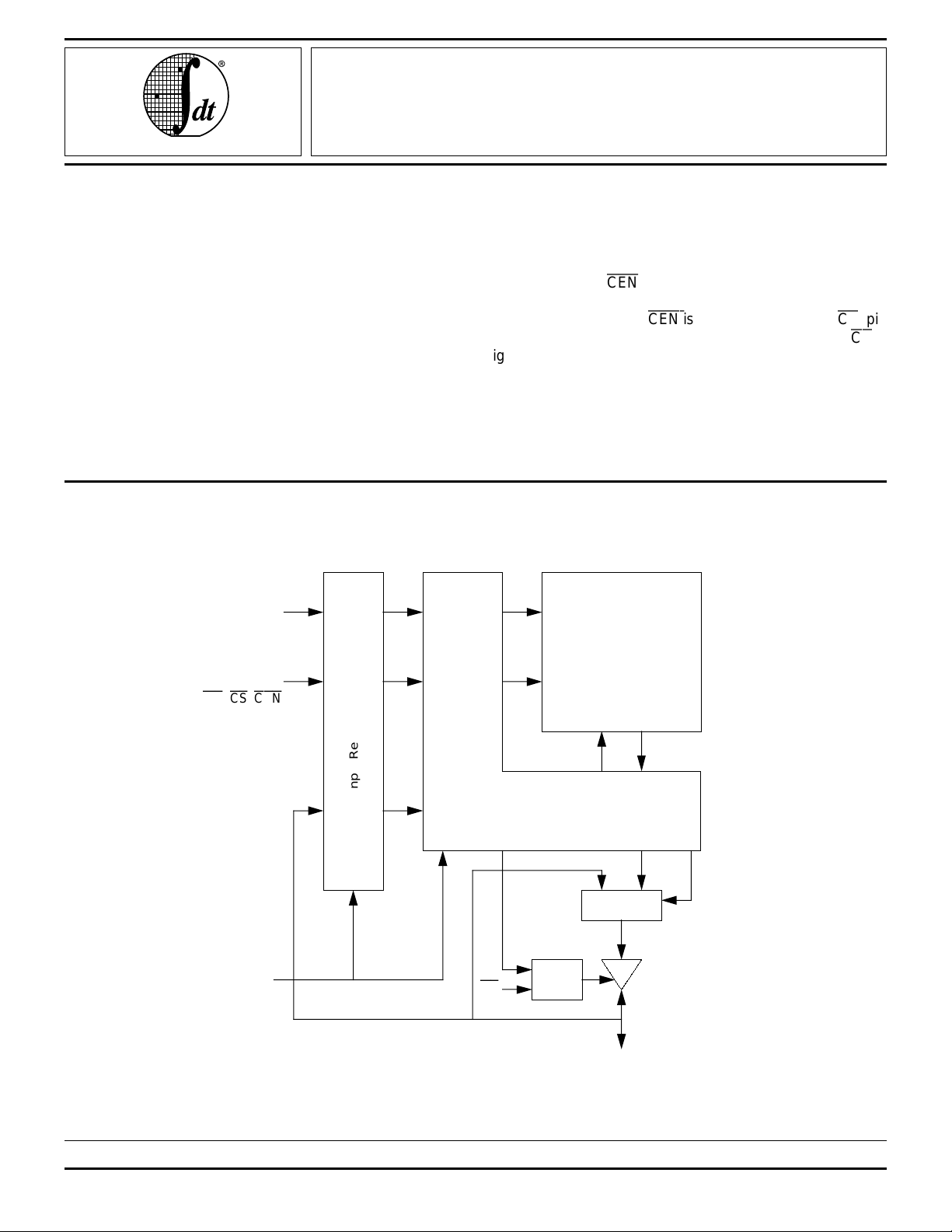
FUNCTIONAL BLOCK DIAGRAM
Address
DQ
during one clock cycle, and one clock cycle later its associated
data cycle occurs, be it read or write.
The IDT71V509 contains data, address, and control signal
registers. Output Enable is the only asynchronous signal, and
can be used to disable the output at any time.
A Clock Enable (
CEN
) pin allows operation of the IDT71V509
to be suspended as long as necessary. All synchronous
inputs are ignored when
CEN
is high. A Chip Select (CS) pin
allows the user to deselect the device when desired. If CS is
high, no new memory operation is initiated, but any pending
data transfers (reads and writes) will still be completed.
The IDT71V509 utilizes IDT's high-performance 3.3V CMOS
process, and is packaged in a JEDEC Standard 400-mil 44lead small outline J-lead plastic package (SOJ) for high board
density.
Address
Control
(WE, CS,
Clock
CEN
SRAM
DQ
)
Input Register
DQ
Clk
Control Logic
OE
Control
Gate
DI DO
Mux
Data
Sel
3618 drw 01
The IDT logo is a registered trademark and CacheRAM, Zero Bus Turnaround and ZBTare trademarks of Integrated Device Technology, Inc.
Pentium is a trademark of Intel Corp.
PowerPC is a trademark of International Business Machines, Inc.
COMMERCIAL TEMPERATURE RANGE AUGUST 1996
1996 Integrated Device Technology, Inc. 11.3 DSC-3618/1
1
Page 2
IDT71V509
128K x 8 3.3V SYNCHRONOUS SRAM WITH ZBT AND FLOW-THROUGH OUTPUT COMMERCIAL TEMPERATURE RANGE
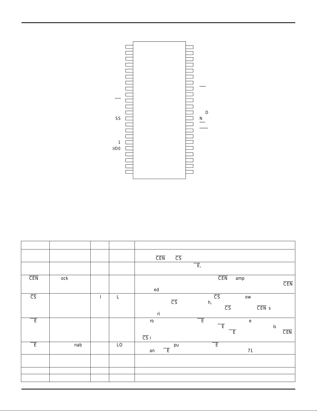
PIN CONFIGURATION
NC
A16
A15
A14
A13
A12
A11
WE
VDD
CLK
VSS
VDD
NC
CS
CEN
A10
A9
A8
A7
A6
A5
NCA4
(4)
(5)
(1)
(3)
10
11
12
13
14
15
16
17
18
19
20
21
22
1
2
3
4
5
6
7
8
9
SO44-1
44
43
42
41
40
39
38
37
36
35
34
33
32
31
30
29
28
27
26
25
24
23
A0
A1
A2
VSS
I/O7
I/O6
VDD
I/O5
I/O4
OE
VDD
VSS
VSS
I/O3
I/O2
VDD
I/O1
I/O0
VSS
(2)
NC
A3
Notes:
1. Pin 32: Future control input
2. Pin 20: Future I/O8
3. Pin 23: Future A17
4. Pin 44: Future A18
5. Pin 36 does not need to be connected directly to VDD, as long as it is ≥ VIH.
3618 drw 02
PIN DEFINITIONS
TOP VIEW
(1)
Symbol Pin Function I/O Active Description
A
0-A16 Address Inputs I N/A Synchronous Address inputs. The address is registered on every rising edge
of CLK if
CEN
and CS are both low.
CLK Clock I N/A The clock input. Except for OE, all input and output timing references for the
device are with respect to the rising edge of CLK.
CEN
Clock Enable I LOW Synchronous clock enable input. When
CEN
is sampled high, the other
synchronous inputs are ignored, and outputs remain unchanged. When
is sampled low, the IDT71V509 operates normally.
CS
Chip Select I LOW Synchronous chip select input. When CS is sampled low, the device operates
normally. When CS is sampled high, no read or write operation is initiated,
and the I/O bus is tri-stated the next cycle. CS is ignored if
CEN
is high at
the same rising edge of CLK.
WE
Write Enable I LOW Synchronous write enable. If WE is sampled low, a write is initiated at the
address that is registered at that time. If WE is sampled high, a read is initiated
at the address that is registered at that time. WE is ignored when either
or CS is sampled high.
OE
Output Enable I LOW Asynchronous output enable. When OE is high, the I/O bus goes high
impedance. OE must be low to read data from the IDT71V509.
I/O
0-I/O7 Data Input/Output I/O N/A Synchronous data input/output (I/O) pins. Both the data input path and data
output path are registered and triggered by the rising edge of CLK.
DD Power Supply N/A N/A 3.3V power supply pins.
V
V
SS Ground N/A N/A Ground pins.
CEN
CEN
11.3 2
Page 3
IDT71V509
128K X 8 3.3V SYNCHRONOUS SRAM WITH ZBT AND FLOW-THROUGH OUTPUT COMMERCIAL TEMPERATURE RANGE
FUNCTIONAL TIMING DIAGRAM
CYCLE
CLOCK
ADDRESS
(A0 - A16)
CONTROL
(CS,
CEN, WE
DATA
(I/O0 - I/O7)
n+29
A29
C29
)
D28
TYPICAL OPERATION -
n+30
A30
C30
D29
CSCS AND
n+31
A31
C31
D30
CEN
ARE LOW
CEN
n+32
A32
C32
D31
n+33
A33
C33
D32
n+34
A34
C34
D33
n+35
A35
C35
D34
n+36
A36
C36
D35
n+37
A37
C37
D36
3618 drw 03
Cycle Address
WE
WE
CSCSCEN
CENOEOE
I/O Comments
n A0 H L L ? D-1 ?
n+1 A1 L L L L D0 Data Out
n+2 A2 H L L X D1 Data In
n+3 A3 L L L L D2 Data Out
n+4 A4 H L L X D3 Data In
n+5 A5 L L L L D4 Data Out
n+6 A6 H L L X D5 Data In
n+7 A7 L L L L D6 Data Out
n+8 A8 H L L X D7 Data In
n+9 A9 L L L L D8 Data Out
n+10 A10 H L L X D9 Data In
n+11 A11 H L L L D10 Data Out
n+12 A12 L L L L D11 Data Out
n+13 A13 L L L X D12 Data In
n+14 A14 H L L X D13 Data In
n+15 A15 H L L L D14 Data Out
n+16 A16 H L L L D15 Data Out
n+17 A17 L L L L D16 Data Out
n+18 A18 L L L X D17 Data In
n+19 A19 L L L X D18 Data In
n+20 A20 H L L X D19 Data In
n+21 A21 H L L L D20 Data Out
11.3 3
Page 4

IDT71V509
128K x 8 3.3V SYNCHRONOUS SRAM WITH ZBT AND FLOW-THROUGH OUTPUT COMMERCIAL TEMPERATURE RANGE
READ OPERATION
Cycle Address
WE
WE
CSCSCEN
CENOEOE
I/O Comments
n A0 H L L X X Address and Control meet setup
n+1 X X X X L D0 Contents of Address A0 Read Out
H = High; L = Low; X = Don’t Care; ? = Don’t Know; Z = High Impedance 3618 tbl 02
WRITE OPERATION
Cycle Address
n A0 L L L X X Address and Control meet setup
n+1 X X X L X D0 New Data Drives SRAM Inputs
H = High; L = Low; X = Don’t Care; ? = Don’t Know; Z = High Impedance 3618 tbl 03
WE
WE
CSCSCEN
CENOEOE
I/O Comments
READ OPERATION WITH CLOCK ENABLE USED
Cycle Address
n A0 H L L X X Address and Control meet setup
n+1 X X X H L D0 Contents of Address A0 Read Out
n+2 A2 H L L L D0 Contents of Address A0 Read Out
n+3 X X X H L D2 Contents of Address A2 Read Out
n+4 X X X H L D2 Contents of Address A2 Read Out
n+5 A5 H L L L D2 Contents of Address A2 Read Out
n+6 A6 H L L L D5 Contents of Address A5 Read Out
n+7 A7 ?LLLD6Contents of Address A6 Read Out
H = High; L = Low; X = Don’t Care; ? = Don’t Know; Z = High Impedance 3618 tbl 04
WE
WE
CSCSCEN
CENOEOE
I/O Comments
WRITE OPERATION WITH CLOCK ENABLE USED
Cycle Address
n A0 L L L X X Address and Control meet setup
n+1 X X X H X X Clock Ignored at n+1 to n+2 Low-to-High
n+2 A2 L L L X D0 New Data Drives SRAM Inputs
n+3 X X X H X X Clock Ignored at n+3 to n+4 Low-to-High
n+4 X X X H X X Clock Ignored at n+4 to n+5 Low-to-High
n+5 A5 L L L X D2 New Data Drives SRAM Inputs
n+6 A6 L L L X D5 New Data Drives SRAM Inputs
n+7 A7 ? L L X D6 New Data Drives SRAM Inputs
H = High; L = Low; X = Don’t Care; ? = Don’t Know; Z = High Impedance 3618 tbl 05
WE
WE
CSCSCEN
CENOEOE
I/O Comments
11.3 4
Page 5

IDT71V509
128K X 8 3.3V SYNCHRONOUS SRAM WITH ZBT AND FLOW-THROUGH OUTPUT COMMERCIAL TEMPERATURE RANGE
READ OPERATION WITH CHIP SELECT USED
Cycle Address
WE
WE
CSCSCEN
CENOEOE
I/O Comments
n X X H L X ? Deselected
n+1 X X H L X Z Deselected
n+2 A2 H L L X Z Address and Control meet setup
n+3 X X H L L D2 Deselected, Contents of Address A2 Read Out
n+4 A4 H L L X Z Address and Control meet setup
n+5 X X H L L D4 Deselected, Contents of Address A4 Read Out
n+6 X X H L X Z Deselected
n+7 A7 H L L X Z Address and Control meet setup
n+8 X X H L L D7 Deselected, Contents of Address A7 Read Out
n+9 X X H L X Z Deselected
H = High; L = Low; X = Don’t Care; ? = Don’t Know; Z = High Impedance 3618 tbl 06
WRITE OPERATION WITH CHIP SELECT USED
Cycle Address
n X X H L X ? Deselected
n+1 X X H L X Z Deselected
n+2 A2 L L L X Z Address and Control meet setup
n+3 X X H L X D2 Deselected, New Data Drives SRAM Inputs
n+4 A4 L L L X Z Address and Control meet setup
n+5 X X H L X D4 Deselected, New Data Drives SRAM Inputs
n+6 X X H L X Z Deselected
n+7 A7 L L L X Z Address and Control meet setup
n+8 X X X L X D7 Deselected, New Data Drives SRAM Inputs
n+9 X X X L X Z Deselected
H = High; L = Low; X = Don’t Care; ? = Don’t Know; Z = High Impedance 3618 tbl 07
WE
WE
CSCSCEN
CENOEOE
I/O Comments
11.3 5
Page 6

IDT71V509
128K x 8 3.3V SYNCHRONOUS SRAM WITH ZBT AND FLOW-THROUGH OUTPUT COMMERCIAL TEMPERATURE RANGE
ABSOLUTE MAXIMUM RATINGS
(1)
Symbol Rating Com’l. Unit
(2)
V
TERM
Terminal Voltage with –0.5 to +4.6 V
Respect to GND
(3)
V
TERM
Terminal Voltage with –0.5 to VDD+0.5 V
Respect to GND
T
A Operating Temperature 0 to +70 °C
BIAS Temperature Under Bias –55 to +125 °C
T
STG Storage Temperature –55 to +125 °C
T
P
T Power Dissipation 1.0 W
I
OUT DC Output Current 50 mA
NOTES:
1. Stresses greater than those listed under ABSOLUTE MAXIMUM
RATINGS may cause permanent damage to the device. This is a stress
rating only and functional operation of the device at these or any other
conditions above those indicated in the operational sections of this
specification is not implied. Exposure to absolute maximum rating
conditions for extended periods may affect reliability.
DD and Input terminals only.
2. V
3. I/O terminals.
RECOMMENDED DC OPERATING
CONDITIONS
Symbol Parameter Min. Typ. Max. Unit
VDD Supply Voltage 3.135 3.3 3.465 V
VSS Supply Voltage 0 0 0 V
VIH Input High Voltage - Inputs 2.0 — 4.6 V
VIH Input High Voltage - I/O 2.0 — VDD+0.3 V
IL Input Low Voltage –0.3
V
NOTE:
IL (min.) = –1.5V for pulse width less than 5 ns, once per cycle.
1. V
(1)
— 0.8 V
CAPACITANCE
(TA = +25°C, f = 1.0MHz, SOJ package)
Symbol Parameter
IN Input Capacitance VIN = 3dV 6 pF
C
I/O I/O Capacitance VOUT = 3dV 7 pF
C
NOTE:
1. This parameter is guaranteed by device characterization, but not production tested.
(1)
Conditions Max. Unit
DC ELECTRICAL CHARACTERISTICS OVER THE OPERATING
TEMPERATURE AND SUPPLY VOLTAGE RANGE
Symbol Parameter Test Condition Min. Max. Unit
LI| Input Leakage Current VDD = Max., VIN = 0V to VDD —5µA
|I
LO| Output Leakage Current
|I
OL Output Low Voltage IOL = 5 mA, VDD = Min. — 0.4 V
V
V
OH Output High Voltage IOH = –5 mA, VDD = Min. 2.4 — V
CS
≥ VIH, VOUT = 0V to VDD, VDD = Max. — 5 µA
(VDD = 3.3V ±5%)
DC ELECTRICAL CHARACTERISTICS OVER THE OPERATING
TEMPERATURE AND SUPPLY VOLTAGE RANGE
Symbol Parameter Test Condition 71V509S66 71V509S50 Unit
DD Operating Power
I
Supply Current V
ISB Standby Power
Supply Current V
ISB1 Full Standby Power
Supply Current V
NOTES:
1. All values are maximum guaranteed values.
2. At f = f
MAX, address inputs are switching at 1/tCYC and CLK is cycling at 1/tCYC; f=0 means no input signals are changing.
CS
≤ VIL, Outputs Open, VDD = Max., 150 120 mA
IN ≥ VIH or ≤ VIL, f = fMAX
CS
≥ VIH, Outputs Open, VDD = Max., 50 45 mA
IN ≥ VIH or ≤ VIL, f = fMAX
CS
≥ VHD, Outputs Open, VDD = Max., 10 10 mA
IN ≥ VHD or ≤ VLD, f = 0
(2)
(1)
(VDD = 3.3V ±5%, VHD = VDD - 0.2V, VLD = 0.2V)
(2)
(2)
11.3 6
Page 7

IDT71V509
128K X 8 3.3V SYNCHRONOUS SRAM WITH ZBT AND FLOW-THROUGH OUTPUT COMMERCIAL TEMPERATURE RANGE
AC ELECTRICAL CHARACTERISTICS
(VDD = 3.3V ±5%, TA = 0 to 70°C)
IDT71V509S66 IDT71V509S50
Symbol Parameter Min. Max. Min. Max. Unit
Clock Parameters
fMAX Clock Frequency — 66 — 50 MHz
CYC Clock Cycle Time 15 — 20 — ns
t
CH Clock High Pulse Width 5 — 6 — ns
t
CL Clock Low Pulse Width 5 — 6 — ns
t
Output Parameters
tCD Clock High to Valid Data — 9 — 10 ns
CDC Clock High to Data Change 2 — 2 — ns
t
(1)
t
CLZ
(1)
CHZ
t
OE Output Enable Access Time — 6 — 7 ns
t
(1)
t
OLZ
(1)
OHZ
t
Clock High to Output Active 2 — 2 — ns
Clock High to Data High-Z 2 5 2 6 ns
Output Enable Low to Data Active 0 — 0 — ns
Output Enable High to Data High-Z — 5 — 6 ns
Set Up Times
tSE Clock Enable Setup Time 2 — 2.5 — ns
SA Address Setup Time 2 — 2.5 — ns
t
SD Data In Setup Time 2 — 2.5 — ns
t
t
SW Write Enable Setup Time 2 — 2.5 — ns
SC Chip Select Setup Time 2 — 2.5 — ns
t
Hold Times
tHE Clock Enable Hold Time 1 — 1 — ns
HA Address Hold Time 1 — 1 — ns
t
t
HD Data In Hold Time 1 — 1 — ns
HW Write Enable Hold Time 1 — 1 — ns
t
t
HC Chip Select Hold Time 1 — 1 — ns
NOTES:
1. Transition is measured ±200mV from steady-state.
AC TEST CONDITIONS
Input Pulse Levels 0 to 3V
Input Rise/Fall Times 2ns
Input Timing Reference Levels 1.5V
Output Timing Reference Levels 1.5V
AC Test Load See Figures 1 and 2
AC TEST LOADS
I/O
Z
Figure 1. AC Test Load
0 = 50
Ω
+1.5V
50
Ω
30pF
3618 drw 04
+3.3V
317
Ω
I/O
351
Ω
Figure 2. AC Test Load
OHZ, tCHZ, tOLZ, and tDC1)
(for t
* Including scope and jig
11.3 7
5pF*
3618 drw 05
Page 8

IDT71V509
128K x 8 3.3V SYNCHRONOUS SRAM WITH ZBT AND FLOW-THROUGH OUTPUT COMMERCIAL TEMPERATURE RANGE
TIMING WAVEFORM OF READ AND WRITE CYCLES
CLK
tSE
tHE
CEN
tSA tHA
ADDRESS
WE
CS
OE
DATA_in
DATA_out
NOTES:
1. Dx represents the data for address Ax.
2. DATA_in and DATA_out together represent I/O(7:0).
A1 A2 A3 A4 A5 A6
tSW tHW
tSC tHC
tSD
tHD
D3
tCLZ
tCD
D2
tCHZ
(1)
D4D1
tCDC
D5
A7 A8
D7
tCD
D6
3618 drw 06
TIMING WAVEFORM OF
CEN
OPERATION
CEN
CLK
CEN
ADDRESS
A1 A3 A5
WE
CS
OE
DATA_in
DATA_out
NOTES:
1. Dx represents the data for address Ax.
2. DATA_in and DATA_out together represent I/O(7:0).
D1 D5D1
(1)
D3
A6 A7
D6
3618 drw 07
11.3 8
Page 9

IDT71V509
128K X 8 3.3V SYNCHRONOUS SRAM WITH ZBT AND FLOW-THROUGH OUTPUT COMMERCIAL TEMPERATURE RANGE
TIMING WAVEFORM OF
CLK
CEN
ADDRESS
WE
CS
OE
DATA_in
DATA_out
A1 A4A2 A7
CSCS OPERATION
D2D1
(1)
D4
3618 drw 08
NOTES:
1. Dx represents the data for address Ax.
2. DATA_in and DATA_out together represent I/O(7:0).
TIMING WAVEFORM OF
OEOE OPERATION
OE
DATA_out
NOTES:
1. A read operation is assumed to be in progress.
ORDERING INFORMATION
71V509IDT
Device
Type
S
Power
X
Speed
Y
Package
tOHZ
tOE
tOLZ
Valid
3618 drw 09
Y
50
66
11.3 9
Small Outline J-Bend, 44 pin (SO44-1)
Clock Frequency in Megahertz
3618 drw 10
 Loading...