

128K x 36, 256K x 18
3.3V Synchronous ZBT SRAMs
3.3V I/O, Burst Counter
Pipelined Outputs
IDT71V3556S
IDT71V3558S
IDT71V3556SA
IDT71V3558SA
Features
◆◆
◆
◆◆
128K x 36, 256K x 18 memory configurations
◆◆
◆
◆◆
Supports high performance system speed - 200 MHz
(3.2 ns Clock-to-Data Access)
◆◆
◆
◆◆
ZBTTM Feature - No dead cycles between write and read
cycles
◆◆
◆
◆◆
Internally synchronized output buffer enable eliminates the
need to control
◆◆
◆
◆◆
Single R/
◆◆
◆
◆◆
Positive clock-edge triggered address, data, and control
OEOE
OE
OEOE
WW
W (READ/WRITE) control pin
WW
signal registers for fully pipelined applications
◆◆
◆
◆◆
4-word burst capability (interleaved or linear)
◆◆
◆
◆◆
Individual byte write (
◆◆
◆
◆◆
Three chip enables for simple depth expansion
◆◆
◆
◆◆
3.3V power supply (±5%), 3.3V I/O Supply (VDDQ)
◆◆
◆
◆◆
Optional- Boundary Scan JTAG Interface (IEEE 1149.1
BWBW
BWBW
BW1 -
BW4) control (May tie active)
BWBW
BWBW
compliant)
◆◆
◆
◆◆
Packaged in a JEDEC standard 100-pin plastic thin quad
flatpack (TQFP), 119 ball grid array (BGA) and 165 fine pitch
ball grid array (fBGA)
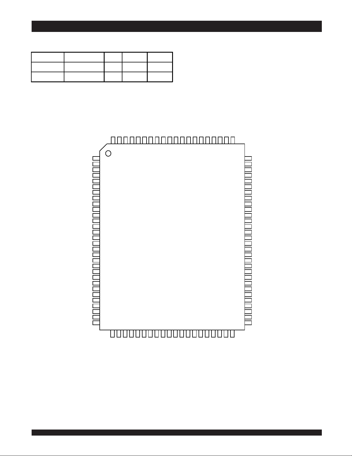
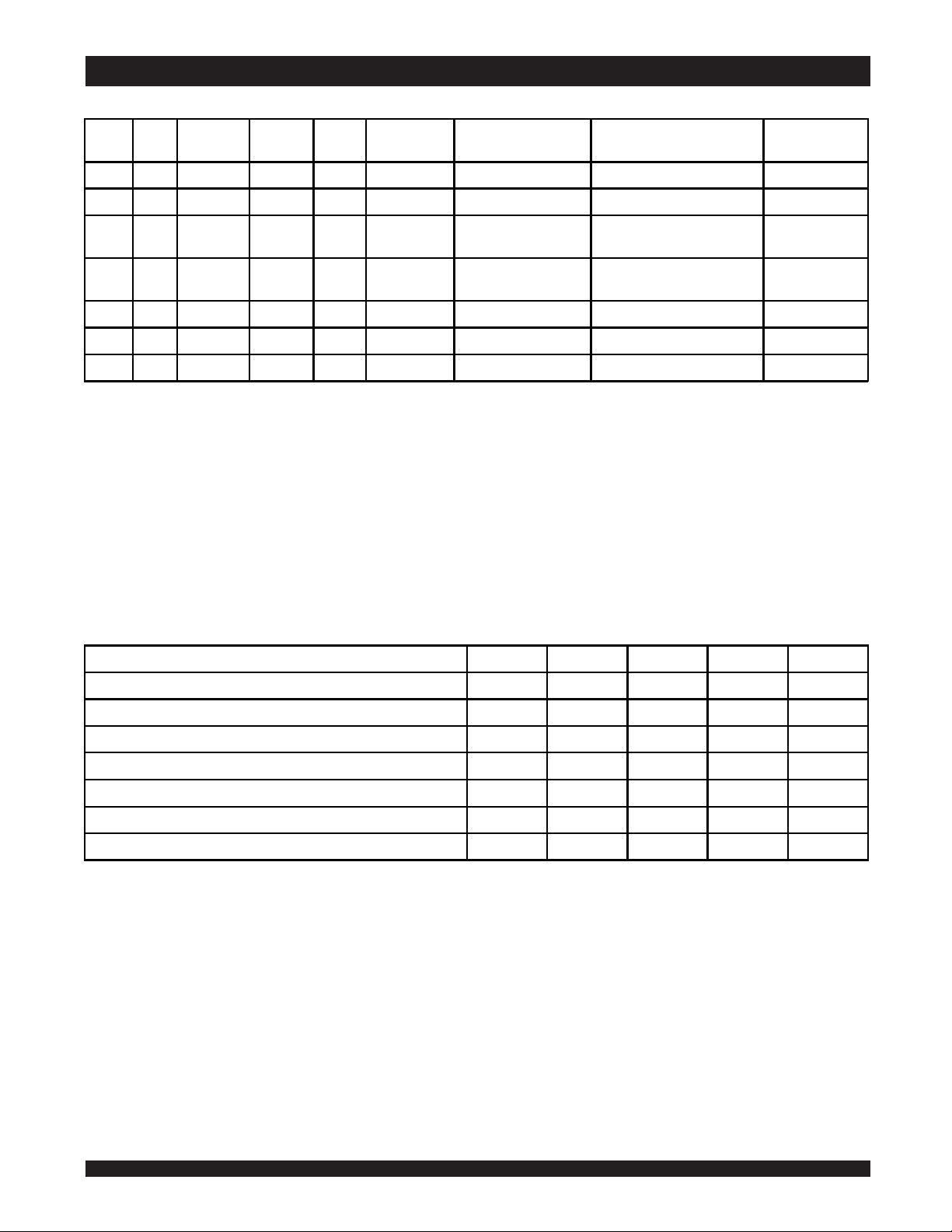
Pin Description Summary
Description
The IDT71V3556/58 are 3.3V high-speed 4,718,592-bit (4.5 Megabit) synchronous SRAMS. They are designed to eliminate dead bus
cycles when turning the bus around between reads and writes, or
writes and reads. Thus, they have been given the name ZBTTM, or
Zero Bus Turnaround.
Address and control signals are applied to the SRAM during one
clock cycle, and two cycles later the associated data cycle occurs, be it
read or write.
The IDT71V3556/58 contain data I/O, address and control signal
registers. Output enable is the only asynchronous signal and can be used
to disable the outputs at any given time.
A Clock Enable (CEN) pin allows operation of the IDT71V3556/58
to be suspended as long as necessary. All synchronous inputs are
ignored when (CEN) is high and the internal device registers will hold
their previous values.
There are three chip enable pins (CE1, CE2, CE2) that allow the user
to deselect the device when desired. If any one of these three are not
asserted when ADV/LD is low, no new memory operation can be
initiated. However, any pending data transfers (reads or writes) will be
completed. The data bus will tri-state two cycles after chip is deselected
or a write is initiated.
17
A0-A
1
CE
OE
W
R/
CEN
BW
CLK Clock Input N/A
ADV/
LBO
TMS Test Mode Select Input Synchronous
TDI Test Data Input Input Synchronous
TCK Test Clock Input N/A
TDO Tes t Data Ou tp ut Outp ut Sync hr on o us
TRST
ZZ Sleep Mode Input Synchronous
0
I/O
VDD, V
SS
V
2
CE
, CE2,
1
2
3
BW
BW
,
,
LD
-I/O31, I/OP1-I/O
DDQ
4
BW
,
P4
Address Inputs Input Synchronous
Chip E nabl es Input Sync hrono us
Output Enable Input Asynchronous
Read /Write Si gnal Input Sy nchro nous
Clock Enable Input Synchronous
Individual Byte Write Selects Input Synchronous
Ad vance b urst add re ss / Lo ad ne w ad dre ss Input Sync hrono us
Linear / Interleaved Burst Order Input Static
JTAG Reset (Optional) Input Asynchronous
Data Inp ut / Ou tp ut I/O Sy nc hr ono u s
Core P owe r, I/ O Po we r Sup p ly Static
Ground Supply Static
SEPTEMBER 2004
5281 tbl 01
©2004 Integrated Device Technology, Inc.
1
DSC-5281/08
IDT71V3556, IDT71V3558, 128K x 36, 256K x 18, 3.3V Synchronous SRAMS with
Symbo l
Pin Function
I/O
Active
Description
ZBT
Feature, 3.3V I/O, Burst Counter, and Pipelined Outputs Commercial and Industrial Temperature Ranges
Description continued
The IDT71V3556/58 has an on-chip burst counter. In the burst
mode, the IDT71V3556/58 can provide four cycles of data for a single
address presented to the SRAM. The order of the burst sequence is
defined by the LBO input pin. The LBO pin selects between linear and
interleaved burst sequence. The ADV/LD signal is used to load a new
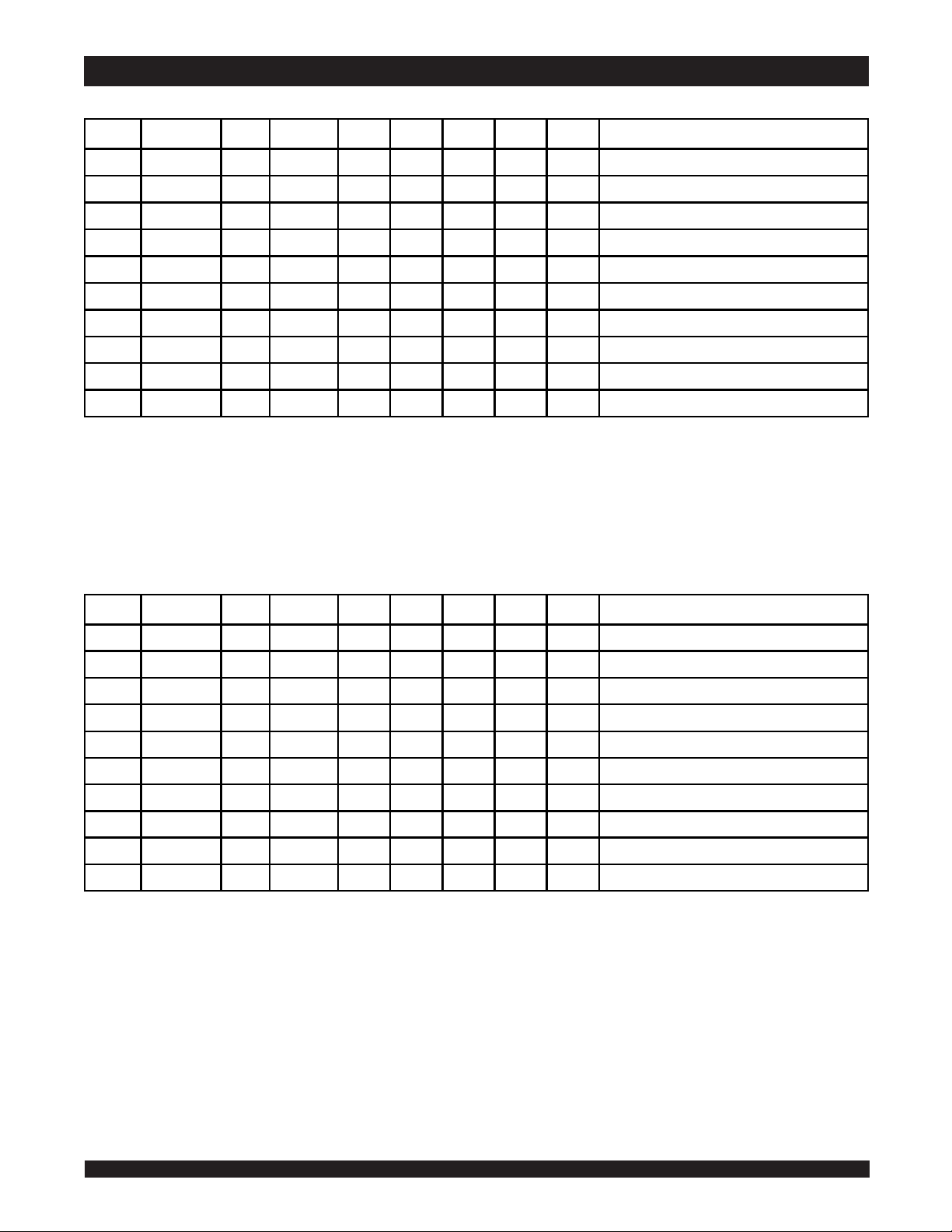
Pin Definition
(1)
external address (ADV/LD = LOW) or increment the internal burst counter
(ADV/LD = HIGH).
The IDT71V3556/58 SRAMs utilize IDT's latest high-performance
CMOS process and are packaged in a JEDEC standard 14mm x 20mm
100-pin thin plastic quad flatpack (TQFP) as well as a 119 ball grid array
(BGA) and a 165 fine pitch ball grid array (fBGA).
17
A0-A
ADV/
LD
R/
W
CEN
1
-
BW
BW
1
,
CE
CE
2
CE
CLK Clock I N/A
I/O
-I/O
0
I/OP1-I/O
LBO
OE
TMS Test Mode Select I N/A Gives input command for TAP controller. Sampled on rising edge of TDK. This pin has an internal pullup.
TDI Test Data Inp ut I N/A
TCK Te st Cloc k I N/A
TDO Tes t Data O utp ut O N/A
TRST
ZZ Sleep Mode I HIGH
DD
V
DDQ
V
SS
V
Address Inputs I N/A
Adv ance / Load I N/A
Read / Write I N/A
Clock Enable I LOW
Ind iv id ua l By te
4
Write Enable s
Chip Enab les I LOW
2
Chip Enab le I HIGH
31
Data Inp ut/ Ou tp ut I/O N/A
P4
Linear Burst O rde r I LOW
Output Enable I LOW
JTAG Reset
(Optional)
Powe r Sup p ly N/A N/A 3.3V c ore p owe r sup p ly.
Power Supply N/A N/A 3.3V I/O Supply.
Ground N/A N/A Ground.
ILOW
ILOW
Synchronous Address inputs. The address register is triggered by a combination of the rising edge of CLK,
low,
ADV/
LD
ADV/
LD
is sampled low at the rising edge of clock with the chip selected. When ADV/
deselected, any burst in progress is terminated. When ADV/
is advanced for any burst that was in progress. The external addresses are ignored when ADV/
high.
signal is a synchronous input that identifies whether the current load cycle initiated is a Read or Write
R/
W
access to the memory array. The data bus activity for the current cycle takes place two clock cycles later.
Synchronous Clock Enable Input. When
ignored and outputs remain unchanged. The effect of
to high clock transition did not occur. For normal operation,
Synchronous byte write enables. Each 9-bit byte has its own active low byte write enable. On load write cycles
(When R/
write signal must also be valid on each cycle of a burst write. Byte Write signals are ignored when R/
sampled high. The appropriate byte(s) of data are written into the device two cycles later.
tied low if always doing write to the entire 36-bit word.
Synchronous active low chip e nable.
2
sampled high or CE2 sampled low) and ADV/LD low at the rising edge of clock, initiates a deselect cycle.
CE
The ZBT
Sync hrono us active high chi p e nable . CE
polarity but otherwise id entical to
This is the cl o ck i np ut to the IDT71V 3556 /58 . E x ce p t fo r
respect to the rising edge of CLK.
Synchronous data input/output (I/O) pins. Both the data input path and data output path are registered and
triggered by the rising edge of CLK.
Burst order se lection input. When
the Linear burst sequence is selected.
Asynchronous output enable.
are in a high-impe danc e state.
operation,
Serial input of registers placed between TDI and TDO. Sampled on rising edge of TCK. This pin has an internal
pullup.
Clock input of TAP controller. Each TAP event is clocked. Test inputs are captured on rising edge of TCK,
while test outputs are d riven from the falling edge of TCK. This pin has an internal pullup.
Serial output of registers placed between TDI and TDO. This output is active depending on the state of the TAP
controller.
Optional Asynchronous JTAG reset. Can be used to reset the TAP co ntroller, but not required. JTAG reset
oc curs automatically at powe r up and als o rese ts using TMS and TCK per IEEE 1149.1. If not used
be le ft floating. This pin has an internal pullup. Only available in BGA package.
Synchronous sleep mode input. ZZ HIGH will gate the CLK internally and power down the IDT71V3556/3558 to
its lowest power consumption level. Data retention is guaranteed in Sleep M ode . This pin has an internal
pulldown.
low, and true chip enab les .
CEN
is a sync hrono us input that is used to l oad the internal reg isters with new addre s s and co ntrol when it
is s a mp le d hi gh then th e i nte rna l b urs t c ou nter
LD
is sampled high, all other synchronous inputs, including clock are
CEN
and ADV/LD are sampled low) the appropriate byte write signal (
W
1
and
CE
CE
TM
has a two cycle deselect, i.e., the data bus will tri-state two clock cycles after deselect is initiated.
2
is used with
1
2
and
.
CE
is high the Interleaved burst sequence is selected. When
is a static input and it must no t change d uring d ev ice op e ration.
LBO
can be tied low.
OE
CE
LBO
must be low to re ad d ata from the 71V3556/58. When OE is high the I/O pins
OE
does not need to be actively controlled for read and write cycles. In normal
OE
sampled high on the device outputs is as if the low
CEN
2
are used with CE2 to enable the IDT71V3556/58. (
must be sampled low at rising edge of clock.
CEN
1
2
and
CE
OE
to enable the chip. CE2 has inverted
CE
, all timing references for the device are made with
is low with the chip
LD
1
4
-
) must be valid. The b y te
BW
BW
NOTE:
1. All synchronous inputs must meet specified setup and hold times with respect to CLK.
6.422
BW
LD
1
-
BW
is sampled
is
W
4
can all be
1
or
CE
is low
LBO
can
TRST
5281 tbl 02
IDT71V3556, IDT71V3558, 128K x 36, 256K x 18, 3.3V Synchronous SRAMS with
ZBT
Feature, 3.3V I/O, Burst Counter, and Pipelined Outputs Commercial and Industrial Temperature Ranges
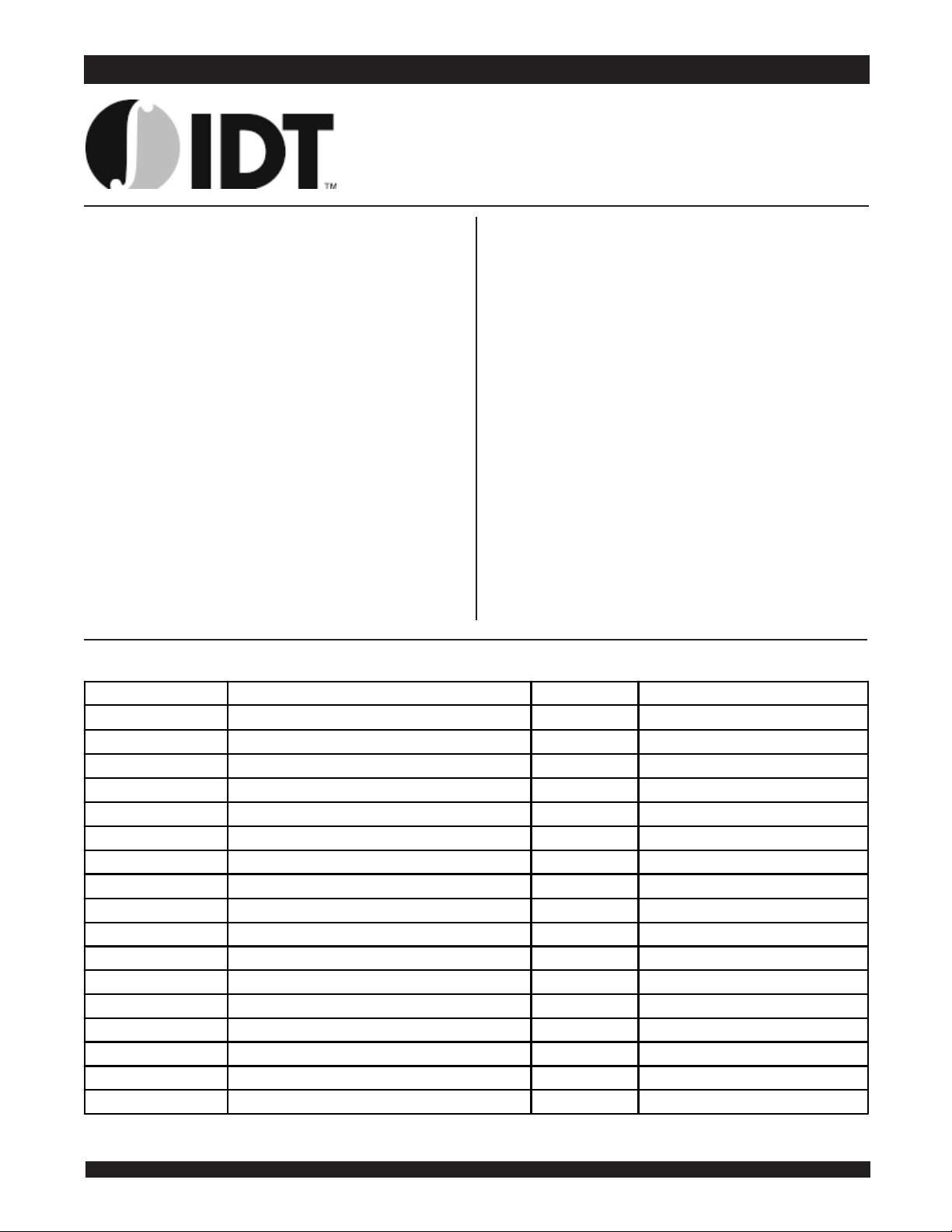
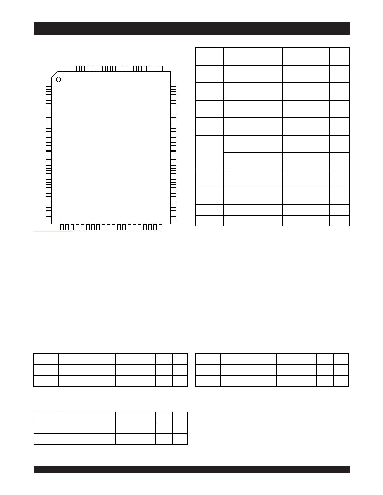
Functional Block Diagram
LBO
Address A [0:16]
CE1, CE2, CE2
R/
CEN
ADV/LD
BW x
Clock
128Kx36 BIT
MEMORY ARRAY
DQ
W
DQ
egist er
Input R
DQ
Clk
Control Logic
Address
Control
Clk
Output Register
DI DO
Mux
D
Q
Sel
OE
TMS
TDI
TCK
TRST
(optional)
JTAG
(SA Version)
TDO
Gate
Data I/O [0:31],
I/O P[1:4]
5281 drw 01a
,
6.42
3
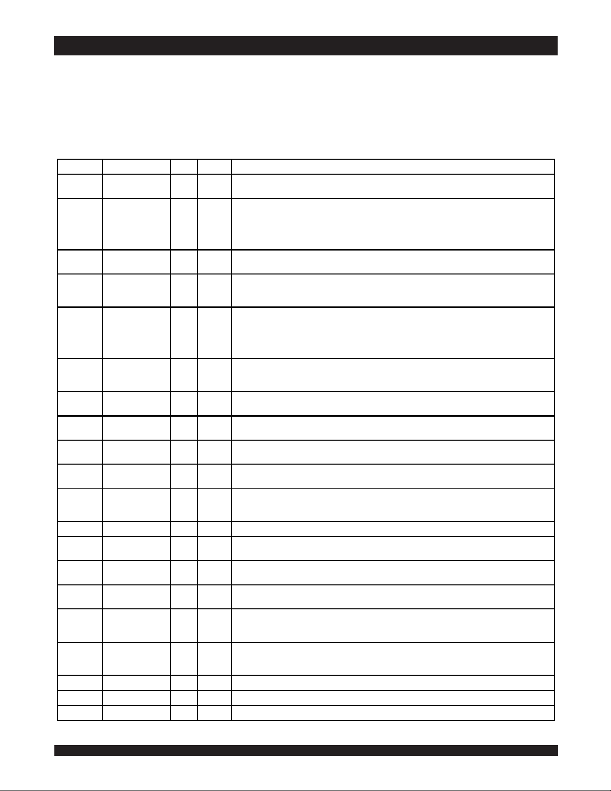
IDT71V3556, IDT71V3558, 128K x 36, 256K x 18, 3.3V Synchronous SRAMS with
(2)
(1)
52 81 tbl 04
ZBT
Feature, 3.3V I/O, Burst Counter, and Pipelined Outputs Commercial and Industrial Temperature Ranges
Functional Block Diagram
Address A [0:17]
CE1, CE2, CE2
ADV/LD
Clock
LBO
R/W
CEN
BW x
DQ
DQ
egiste r
Input R
DQ
Clk
Control Logic
Clk
256x18 BIT
MEMORY ARRAY
Address
Control
DI DO
Mux
D
Output Register
Q
Sel
OE
TMS
TDI
TCK
TRST
(optional)
JTAG
(SA Version)
Recommended DC Operating
Conditions
Symbol Parameter Min. Typ. Max. Unit
Core Sup p ly Voltag e 3.135 3.3 3.465 V
V
DD
I/O S up p ly Vo lta ge 3. 135 3.3 3.465 V
V
DDQ
Supply Voltage 0 0 0 V
V
SS
Inp ut Hig h Vo l tag e - Inputs 2.0
V
IH
Input High Voltage - I/O 2.0
V
IH
Input Lo w Vol tage -0.3
V
IL
NOTES:
1. VIL (min.) = –1.0V for pulse width less than tCYC/2, once per cycle.
2. VIH (max.) = +6.0V for pulse width less than tCYC/2, once per cycle.
____
V
+0.3 V
DD
____
V
+0.3
DDQ
____
0.8 V
Gate
5281drw 01b
,
Data I/O [0:15],
TDO
V
I/O P[ 1:2]
6.424
IDT71V3556, IDT71V3558, 128K x 36, 256K x 18, 3.3V Synchronous SRAMS with
Grade
Temperature
(1)
VSSVDDV
DDQ
ZBT
Feature, 3.3V I/O, Burst Counter, and Pipelined Outputs Commercial and Industrial Temperature Ranges
Recommended Operating
Temperature and Supply Voltage
Comm ercial 0°C to +70°C 0V 3.3V± 5% 3.3V± 5%
Ind us tria l - 40° C to + 85°C 0 V 3.3V ±5% 3. 3V ± 5%
NOTES:
5281 tbl 05
1. TA is the "instant on" case temperature.
Pin Configuration - 128K x 36
D
L
4
3
2
A6A
100 99 9 8 97 96 95 94 93 92 91 90 87 86 85 84 83 82 8189 88
B
C
C
2
1
7
E
W
E
1
2
D
S
LK
D
W
W
W
B
B
B
S
E
C
C
V
V
W
/
R
/
(2)
(2)
V
N
E
C
C
D
E
A
N
O
C
9
A8A
N
DDQ
V
SS
V
SS
DDQ
DD
V
SS
V
DDQ
V
SS
SS
V
DDQ
1
P3
2
16
3
17
4
5
6
18
7
19
8
20
9
21
10
11
12
22
13
23
(1)
14
15
(1)
16
17
18
24
19
25
20
21
22
26
23
27
24
28
25
29
26
27
28
30
29
31
30
P4
31 32 33 34 35 36 37 38 39 40 41 42 43 44 45 46 47 48 49 50
O
LB
5
A0A1A2A3A4A
S
C
N
D
C
N
C
S
V
C
D
N
N
V
I/O
I/O
I/O
V
I/O
I/O
I/O
I/O
V
I/O
I/O
V
DD
V
DD
I/O
I/O
V
I/O
I/O
I/O
I/O
V
I/O
I/O
I/O
80
I/O
I/O
I/O
V
V
I/O
I/O
I/O
I/O
V
V
I/O
I/O
V
V
V
VSS/ZZ
I/O
I/O
V
V
I/O
I/O
I/O
I/O
V
V
I/O
I/O
I/O
5281 drw 02
15
14
DDQ
SS
13
12
11
10
SS
DDQ
9
8
SS
DD
DD
7
6
DDQ
SS
5
4
3
2
SS
DDQ
1
0
P2
(1)
(3)
,
P1
79
78
77
76
75
74
73
72
71
70
69
68
67
66
65
64
63
62
61
60
59
58
57
56
55
54
53
52
51
14A13A12A11A10
16
A15A
A
Top View
100 TQFP
NOTES:
1. Pins 14, 16 and 66 do not have to be connected directly to VDD as long as the input voltage is ≥ VIH.
2. Pins 83 and 84 are reserved for future 8M and 16M respectively.
3. Pin 64 does not have to be connected directly to VSS as long as the input voltage is ≤ VIL; on the latest die revision this
pin supports ZZ (sleep mode).
6.42
5
IDT71V3556, IDT71V3558, 128K x 36, 256K x 18, 3.3V Synchronous SRAMS with
Symbol
Rati ng
Commercial &
Industrial Values
Uni t
TERM
TERM
DD
TERM
TERM
DDQ
A
Commercial
Industrial
BIAS
STG
T
OUT
Symbol
Parameter
(1)
Conditions
Max.
Unit
CINInp ut Cap ac itanc e
VIN = 3dV
5pFC
I/O
I/O Cap aci tanc e
V
OUT
= 3dV
7
pF
5281 tbl 07
Symbol
Par a me t e r
(1)
Conditions
Max .
Unit
CINInput Cap aci tance
VIN = 3dV
7pFC
I/O
I/O Cap aci tance
V
OUT
= 3dV
7
pF
5281 tbl 07 a
Symb ol
Par a me t e r
(1)
Con dit ions
Max .
Unit
CINInp ut Cap ac itanc e
VIN = 3dV
TBDpFC
I/O
I/O Cap ac itance
V
OUT
= 3dV
TBD
pF
5281 tb l 07b
ZBT
Feature, 3.3V I/O, Burst Counter, and Pipelined Outputs Commercial and Industrial Temperature Ranges
Pin Configuration - 256K x 18
LD
2
2
1
7
E
E
A6A
C
C
10099989796959493929190 8786858483828189 88
1
NC
2
NC
3
NC
4
DDQ
V
5
SS
V
6
NC
7
NC
8
8
I/O
9
9
I/O
10
SS
V
11
DDQ
V
12
10
I/O
13
11
I/O
(1)
14
DD
V
15
DD
V
(1)
16
DD
V
17
SS
V
18
12
I/O
19
13
I/O
20
DDQ
V
21
SS
V
22
14
I/O
23
15
I/O
24
P2
I/O
25
NC
26
V
SS
27
DDQ
V
28
NC
29
NC
30
NC
31 32 33 34 35 36 37 38 39 40 41 42 43 44 45 46 47 48 49 50
5
O
LB
1
2
D
S
C
C
W
W
B
B
N
N
C
A0A1A2A3A4A
N
LK
D
S
E
C
V
V
C
S
C
D
C
S
D
N
N
V
V
/
(2)
(2)
V
N
W
E
C
D
E
/
A
O
C
R
C
N
9
C
A8A
N
N
80
79
78
77
76
75
74
73
72
71
70
69
68
67
66
65
64
63
62
61
60
59
58
57
56
55
54
53
52
51
5281 drw 02a
15A14A13A12A11
17
A
A16A
Top View
100 TQFP
NOTES:
1. Pins 14, 16 and 66 do not have to be connected directly to VDD as long as
the input voltage is ≥ VIH.
2. Pins 83 and 84 are reserved for future 8M and 16M respectively.
3. Pin 64 does not have to be connected directly to VSS as long as the input
voltage is ≤ VIL; on the latest die revision this pin supports ZZ (sleep
mode).
Absolute Maximum Ratings
(2)
V
10
A
NC
NC
V
V
NC
I/O
I/O
I/O
V
V
I/O
I/O
V
V
V
VSS/ZZ
I/O
I/O
V
V
I/O
I/O
NC
NC
V
V
NC
NC
NC
DDQ
SS
SS
DDQ
SS
DD
DD
DDQ
SS
SS
DDQ
V
V
P1
7
6
V
5
4
(1)
(7)
T
(3)
3
2
T
1
0
T
,
P
I
NOTES:
1. Stresses greater than those listed under ABSOLUTE MAXIMUM RATINGS may
cause permanent damage to the device. This is a stress rating only and functional
operation of the device at these or any other conditions above those indicated
in the operational sections of this specification is not implied. Exposure to absolute
maximum rating conditions for extended periods may affect reliability.
2. VDD terminals only.
3. VDDQ terminals only.
4. Input terminals only.
5. I/O terminals only.
6. This is a steady-state DC parameter that applies after the power supply has
reached its nominal operating value. Power sequencing is not necessary;
however, the voltage on any input or I/O pin cannot exceed VDDQ during power
Termi nal Voltage with
-0.5 to +4.6 V
Re sp e c t to GN D
(3,6)
Termi nal Voltage with
-0.5 to V
Re sp e c t to GN D
(4,6)
Termi nal Voltage with
-0.5 to VDD +0.5 V
Re sp e c t to GN D
(5,6)
Termi nal Voltage with
-0.5 to V
Re sp e c t to GN D
-0 to + 70
Operating Temperature
-40 to +85
Operating Temperature
Temperature
-55 to +125
Under Bias
Storage
-55 to +125
Temperature
Po we r Dis s ip a tio n 2. 0 W
DC Outp u t Curre nt 50 mA
+0.5 V
supply ramp up.
7. TA is the "instant on" case temperature.
(1)
V
o
C
o
C
o
C
o
C
5281 tbl 06
100 Pin TQFP Capacitance
(1)
(TA = +25° C, f = 1.0MHz)
165 fBGA Capacitance
(1)
(TA = +25° C, f = 1.0MHz)
NOTE:
1. This parameter is guaranteed by device characterization, but not production tested.
6.426
119 BGA Capacitance
(TA = +25° C, f = 1.0MHz)
(1)
IDT71V3556, IDT71V3558, 128K x 36, 256K x 18, 3.3V Synchronous SRAMS with
ZBT
Feature, 3.3V I/O, Burst Counter, and Pipelined Outputs Commercial and Industrial Temperature Ranges
Pin Configuration - 128K x 36, 119 BGA
1234567
DDQ
A V
NC CE
B
NC
C
16
I/O
D
17
I/O
E
DDQ
V
F
20
I/O
G
22
H I/O
DDQ
J V
24
I/O
K
25
L I/O
DDQ
M V
29
N I/O
31
P I/O
R NC A
T NC NC A
DDQ
V
U
A
A
I/O
I/O
I/O
I/O
I/O
DD
V
I/O
I/O
I/O
I/O
I/O
NC/TMS
6
2
7
P3
18
19
21
23
26
27
28
30
P4
5
(3)
A
A
A
V
V
V
BW
V
V
V
BW
V
V
V
LBO
NC/TDI
4
3
2
SS
SS
SS
3
SS
DD(1)
SS
4
SS
SS
SS
10
(3)
NC(2)
LD
ADV/
DD
V
NC V
1
CE
OE
NC(2)
R/W
DD
V
CLK V
NC
CEN
1
A
0
A
DD
V
11
A
NC/TCK
(3)
8
A
9
A
12
A
SS
SS
V
SS
V
BW
SS
V
DD(1)
V
SS
BW
SS
V
SS
V
SS
V
V
14
A
NC/TDO
2
1
DD(1)
(3)
16
A
2
CE
15
A
P2
I/O
13
I/O
12
I/O
11
I/O
9
I/O
DD
V
6
I/O
4
I/O
3
I/O
2
I/O
P1
I/O
13
A
NC NC/ZZ
(3,4)
NC/TRST
DDQ
V
NC
NC
15
I/O
14
I/O
DDQ
V
10
I/O
8
I/O
DDQ
V
7
I/O
5
I/O
DDQ
V
1
I/O
0
I/O
NC
DDQ
V
5281 drw 13A
,
(5)
Top View
Pin Configuration - 256K x 18, 119 BGA
1234567
DDQ
V
A
NC CE2 A
B
NC
C
8
I/O
D
NC I/O
E
DDQ
V
F
NC I/O
G
11
I/O
H
DDQ
V
J
NC I/O
K
13
I/O
L
DDQ
V
M
15
I/O
N
NC I/O
P
NC A
R
NC A
T
DDQ
V
U
6
A
7
A
NC V
9
NC V
10
NC V
DD
V
12
NC NC
14
I/O
NC V
P2
5
10
NC/TMS
(3)
A
A
SS
SS
V
SS
BW
SS
DD(1)
V
SS
V
SS
V
SS
V
SS
SS
V
LBO
15
A
NC/TDI
4
3
2
2
(3)
NC(2)
ADV/LD
DD
V
NC V
CE
1
OE
NC(2)
R/
W
DD
V
CLK V
CEN
1
A
0
A
DD
V
NC A
NC/TCK
(3)
Top View
8
A
9
A
13
A
SS
SS
V
SS
V
SS
V
SS
V
DD(1)
V
SS
BW
SS
V
SS
V
SS
V
V
DD(1)
14
NC/TDO
1
(3)
16
A
2
CE
17
A
P1
I/O
NC I/O
6
I/O
NC I/O
4
I/O
DD
V
NC I/O
2
I/O
NC V
1
I/O
NC I/O
12
A
11
A
(3,4)
NC/TRST
DDQ
V
NC
NC
NC
7
DDQ
V
5
NC
DDQ
V
3
NC
DDQ
NC
0
NC
NC/ZZ
DDQ
V
5281drw13B
(5)
,
NOTES:
1. J3, J5, and R5 do not have to be directly connected to VDD as long as the input voltage is ≥ VIH.
2. G4 and A4 are reserved for future 8M and 16M respectively.
3. These pins are NC for the "S" version or the JTAG signal listed for the "SA" version.
4. TRST is offered as an optional JTAG reset if required in the application. If not needed, can be left floating and will internally be pulled to VDD.
5. Pin T7 does not have to be connected directly to VSS as long as the input voltage is ≤ VIL; on the latest die revision this pin supports ZZ (sleep mode).
6.42
7
IDT71V3556, IDT71V3558, 128K x 36, 256K x 18, 3.3V Synchronous SRAMS with
7
3BW2CE2
8
6CE2BW4BW1
9
DDQVSSVSSVSSVSSVSSVDDQ
P2
16VDDQVDDVSSVSSVSSVDDVDDQ
15
14
18VDDQVDDVSSVSSVSSVDDVDDQ
13
12
20VDDQVDDVSSVSSVSSVDDVDDQ
11
10
22VDDQVDDVSSVSSVSSVDDVDDQ
9
8
DD
DD
DDVSSVSSVSSVDD
24VDDQVDDVSSVSSVSSVDDVDDQ
7
6
26VDDQVDDVSSVSSVSSVDDVDDQ
5
4
28VDDQVDDVSSVSSVSSVDDVDDQ
3
2
30VDDQVDDVSSVSSVSSVDDVDDQ
1
0
DDQVSS
NC/
DD
SSVDDQ
P1
5A2
1
10A13A14
4A3
0
11A12A15A16
5281 tbl 25
7CE1BW2
2
8A10
2
1
9
DDQVSSVSSVSSVSSVSSVDDQ
P1
DDQVDDVSSVSSVSSVDDVDDQ
7
DDQVDDVSSVSSVSSVDDVDDQ
6
DDQVDDVSSVSSVSSVDDVDDQ
5
DDQVDDVSSVSSVSSVDDVDDQ
4
DD
DD
DDVSSVSSVSSVDD
DDQVDDVSSVSSVSSVDDVDDQ
3
DDQVDDVSSVSSVSSVDDVDDQ
2
DDQVDDVSSVSSVSSVDDVDDQ
1
DDQVDDVSSVSSVSSVDDVDDQ
0
DDQVSS
NC/
DD
SSVDDQ
5A2
1
11A14A15
4A3
0
12A13A16A17
5281 tbl 25a
ZBT
Feature, 3.3V I/O, Burst Counter, and Pipelined Outputs Commercial and Industrial Temperature Ranges
Pin Configuration - 128K x 36, 165 fBGA
1234567891011
ANC
(2)
A
BNC A
CI/OP3NC V
DI/O17I/O
EI/O19I/O
FI/O21I/O
GI/O23I/O
HV
(1)
(1)
V
JI/O25I/O
KI/O27I/O
LI/O29I/O
MI/O31I/O
NI/OP4NC V
NC
(2)
(2)
PNCNC
R
LBO
CE1 BW
NC V
A
A
TRST
NC/TDI
NC/TMS
(3, 4)
(3)
(3)
CLK R/
NC V
A
NC/TDO
A
NC/TCK
CEN
LD
ADV/
W
OE
(1)
V
(3)
A
(3)
A
(2)
NC
NC
(2)
A
A
NC
NC I/O
I/O
I/O
I/O
I/O
I/O
I/O
I/O
NC NC NC/ZZ
I/O
I/O
I/O
I/O
NC I/O
NC
I/O
I/O
I/O
I/O
I/O
NC
(2)
(5)
Pin Configuration - 256K x 18, 165 fBGA
1234567891011
ANC
(2)
BNC A6CE
CNC NCV
DNC I/O8V
ENC I/O9V
FNCI/O10V
GNC I/O11V
HV
(1)
JI/O12NC V
KI/O13NC V
LI/O14NC V
MI/O15NC V
NI/OP2NC V
PNC NC
R
LBO
A
NC
(1)
V
(2)
(2)
NC
NC V
A
A
NC
BW
TRST
NC/TDI
NC/TMS
(3, 4)
(3)
(3)
CE
CLK R/
NC V
A
A
CEN
W
NC/TDO
NC/TCK
ADV
/LD
OE
NC
NC
(2)
(2)
A
A
NC
(2)
NC I/O
NC I/O
NC I/O
NC I/O
NC I/O
NC NC NC/ZZ
I/O
I/O
I/O
I/O
(1)
V
(3)
A
(3)
A
NC NC
(5)
NC
NC
NC
NC
NC
NOTES:
1. H1, H2, and N7 do not have to be directly connected to VDD as long as the input voltage is ≥ VIH.
2. A9, B9, B11, A1, R2 and P2 are reserved for future 9M, 18M, 36M, 72M, 144M and 288M respectively.
3. These pins are NC for the "S" version or the JTAG signal listed for the "SA" version.
4. TRST is offered as an optional JTAG reset if required in the application. If not needed, can be left floating and will internally be pulled to VDD.
5. Pin H11 does not have to be connected directly to VSS as long as the input voltage is ≤ VIL; on the latest die revision this pin supports ZZ (sleep mode).
6.428
IDT71V3556, IDT71V3558, 128K x 36, 256K x 18, 3.3V Synchronous SRAMS with
R/WChip
(5)
Enable
ADV/
x
ADDRESS
USED
PREVIOUS CYCLE
CURRENT CYCLE
I/O
(2 cycles l ater)
OP E RATIO N
R/
1BW2BW3
(3)
4
(3)
P3
ZBT
Feature, 3.3V I/O, Burst Counter, and Pipelined Outputs Commercial and Industrial Temperature Ranges
Synchronous Truth Table
CEN
LD
(1)
BW
D
Q
HiZ
(7)
(7)
(7)
(7)
L L S ele ct L Valid Ex ternal X LOAD WRITE D
L H Se lect L X External X LOAD READ Q
L X X H Va lid Internal LOA D WRITE /
BURS T WRITE
L X X H X Inte rna l LOAD RE AD /
BURST READ
L X Deselect L X X X DESELECT or STOP
BURS T WRITE
(Advance burst counter)
BURST READ
(Advance burst counter)
(2)
(2)
(3)
L X X H X X DESELECT / NOOP NOOP HiZ
H X X X X X X SUSP E ND
NOTES:
1. L = VIL, H = VIH, X = Don’t Care.
2. When ADV/LD signal is sampled high, the internal burst counter is incremented. The R/W signal is ignored when the counter is advanced. Therefore the nature of
the burst cycle (Read or Write) is determined by the status of the R/W signal when the first address is loaded at the beginning of the burst cycle.
3. Deselect cycle is initiated when either (CE1, or CE2 is sampled high or CE2 is sampled low) and ADV/LD is sampled low at rising edge of clock. The data bus will
tri-state two cycles after deselect is initiated.
4. When CEN is sampled high at the rising edge of clock, that clock edge is blocked from propogating through the part. The state of all the internal registers and the I/
Os remains unchanged.
5. To select the chip requires CE1 = L, CE2 = L, CE2 = H on these chip enables. Chip is deselected if any one of the chip enables is false.
6. Device Outputs are ensured to be in High-Z after the first rising edge of clock upon power-up.
7. Q - Data read from the device, D - data written to the device.
(4)
Previous Value
5281 tbl 08
Partial Truth Table for Writes
(1)
W
BW
BW
READ HXXXX
WRITE ALL BYTES LLLL L
WRITE BYTE 1 (I/O[0:7], I/OP1)
WRITE BYTE 2 (I/O[8:15], I/OP2)
WRITE BY TE 3 (I/O[16:23], I/ O
WRITE BY TE 4 (I/O[24:31], I/ OP4)
(2)
(2)
(2,3)
)
(2,3)
LLHHH
LHLHH
LHHLH
LHHHL
NO WRITE L HHHH
NOTES:
1. L = VIL, H = VIH, X = Don’t Care.
2. Multiple bytes may be selected during the same cycle.
3. N/A for X18 configuration.
5281 tbl 09
6.42
9

IDT71V3556, IDT71V3558, 128K x 36, 256K x 18, 3.3V Synchronous SRAMS with
Sequence 1
Sequence 2
Sequence 3
Sequence 4
A1A0A1A0A1A0A1
A0
Sequence 1
Sequence 2
Sequence 3
Sequence 4
A1A0A1A0A1A0A1
A0
ZBT
Feature, 3.3V I/O, Burst Counter, and Pipelined Outputs Commercial and Industrial Temperature Ranges
Interleaved Burst Sequence Table (LBO=V
DD)
First Address 0 0 0 1 1 0 1 1
Second Address 0 1 0 0 1 1 1 0
Third Address 1 0 1 1 0 0 0 1
Fourth Address
NOTE:
1. Upon completion of the Burst sequence the counter wraps around to its initial state and continues counting.
(1)
11100100
Linear Burst Sequence Table (LBO=VSS)
First Address 0 0 0 1 1 0 1 1
Second Address 0 1 1 0 1 1 0 0
Third Address 1 0 1 1 0 0 0 1
Fourth Address
NOTE:
1. Upon completion of the Burst sequence the counter wraps around to its initial state and continues counting.
(1)
11000110
5281 tbl 10
5281 tbl 11
Functional Timing Diagram
CYCLE
CLOCK
ADDRESS
(A0 - A16)
CONTROL
(R/W ,ADV/LD , BW x)
DATA
I/O [0:31], I/O P[1:4]
NOTES:
1. This assumes CEN, CE1, CE2, CE2 are all true.
2. All Address, Control and Data_In are only required to meet set-up and hold time with respect to the rising edge of clock. Data_Out is valid after a clock-to-data
delay from the rising edge of clock.
(2)
(2)
(2)
n+29
A29
C29
D/Q27
n+30
A30
C30
D/Q28
(1)
D/Q29
n+31
A31
C31
n+32
A32
C32
D/Q30
n+33
A33
C33
D/Q31
n+34
A34
C34
D/Q32
n+35
A35
C35
D/Q33
n+36
A36
C36
D/Q34
n+37
A37
C37
D/Q35
5281 drw 03
,
6.4210

IDT71V3556, IDT71V3558, 128K x 36, 256K x 18, 3.3V Synchronous SRAMS with
Cycl e
Address
R/WADV/
(1)
xOEI/O
Comments
1
0+1
2
2
3
2+1
4
3+1
4
5
6
7
8
7+1
9
Cycl e
Address
R/WADV/
(2)
xOEI/O
Comments
0
ZBT
Feature, 3.3V I/O, Burst Counter, and Pipelined Outputs Commercial and Industrial Temperature Ranges
Device Operation - Showing Mixed Load, Burst,
CE
(2)
CEN BW
Deselect and NOOP Cycles
LD
nA0H L L L X X X Load read
n+1 X X H X L X X X B urst re ad
n+2 A
n+3 X X L H L X L Q
n+4 X X H XLXLQ1NOOP
n+5 A
n+6 X X H X L X X Z B urst read
n+7 X X L H L X L Q
n+8 A
n+9 X X H X L L X Z B urst write
n+10 A
n+11 X X L H L X X D
n+12 X X H X L X X D
n+13 A
HL LLXLQ0Load read
H L L L X X Z Load read
L L LLLLQ
L L LLLXD3Load write
L L LLLXZLoad write
Deselect or STOP
Deselect or STOP
Load write
Deselect or STOP
NOOP
n+14 A
n+15 A
H L L L X X Z Load read
L L LLLXD5Load write
n+16 X X H XLLLQ6Burst write
n+17 A
n+18 X X H X L X X D
n+19 A
NOTES:
1. CE = L is defined as CE1 = L, CE2 = L and CE2 = H. CE = H is defined as CE1 = H, CE2 = H or CE2 = L.
2. H = High; L = Low; X = Don’t Care; Z = High Impedance.
Read Operation
HL LLXXD7Load read
Burst re ad
L L LLLLQ8Load write
(1)
LD
CE
CEN BW
nA0H L L L X X X Address and Control meet setup
n+1 X X X X L X X X Clock Setup Valid
n+2 X X X XXXLQ
NOTES:
1. H = High; L = Low; X = Don’t Care; Z = High Impedance.
2. CE = L is defined as CE1 = L, CE2 = L and CE2 = H. CE = H is defined as CE1 = H, CE2 = H or CE2 = L.
Contents of Address A0 Re ad Out
5281 tbl 12
5281 tbl 13
6.42
11

IDT71V3556, IDT71V3558, 128K x 36, 256K x 18, 3.3V Synchronous SRAMS with
Cycl e
Address
R/WADV/
(2)
xOEI/O
Comments
0+1
0+1
0+2
0+2
1
0+3
0+3
1
2
1+1
1+1
2
Cycl e
Address
R/WADV/
(2)
xOEI/O
Comments
0
Cycl e
Address
R/WADV/
(2)
xOEI/O
Comments
0+1
0+1
0+2
0+2
0+3
0+3
1
2
1+1
1+1
2
ZBT
Feature, 3.3V I/O, Burst Counter, and Pipelined Outputs Commercial and Industrial Temperature Ranges
LD
(1)
CE
CEN BW
Burst Read Operation
nA0H L L L X X X Address and Control meet setup
n+1 X X H X L X X X Clock Setup Valid, Advance Counter
n+2 X X H XLXLQ0Address A0 Re ad Out, Inc . Co unt
n+3 X X H XLXLQ
n+4 X X H XLXLQ
n+5 A
HL LLXLQ
Address A
Address A
Address A
Re ad Out, Inc . Co unt
Re ad Out, Inc . Co unt
Read Out, Load A
n+6 X X H XLXLQ0Address A0 Re ad Out, Inc . Co unt
n+7 X X H XLXLQ1Address A1 Re ad Out, Inc . Co unt
n+8 A
NOTES:
1. H = High; L = Low; X = Don’t Care; Z = High Impedance..
2. CE = L is defined as CE1 = L, CE2 = L and CE2 = H. CE = H is defined as CE1 = H, CE2 = H or CE2 = L.
Write Operation
HL LLXLQ
Address A
(1)
LD
CE
CEN BW
Read Out, Load A
nA0L L L L L X X Address and Control meet setup
n+1 X X X X L X X X Clock Setup Valid
n+2 X X X X L X X D0Write to Address A
NOTES:
1. H = High; L = Low; X = Don’t Care; Z = High Impedance.
2. CE = L is defined as CE1 = L, CE2 = L and CE2 = H. CE = H is defined as CE1 = H, CE2 = H or CE2 = L.
5281 tbl 14
5281 tbl 15
LD
(1)
CE
CEN BW
Burst Write Operation
nA0L L L L L X X Address and Control meet setup
n+1 X X H X L L X X Clock Setup Valid, Inc. Count
n+2 X X H X L L X D0Address A0 Write, Inc. Co unt
n+3 X X H X L L X D
n+4 X X H X L L X D
n+5A1LLLLLXD
Address A
Address A
Address A
Write, Inc. Co unt
Write, Inc. Co unt
Write, Lo ad A
n+6 X X H X L L X D0Address A0 Write, Inc. Count
n+7 X X H X L L X D1Address A1 Write, Inc. Count
n+8 A
NOTES:
1. H = High; L = Low; X = Don’t Care; ? = Don’t Know; Z = High Impedance.
2. CE = L is defined as CE1 = L, CE2 = L and CE2 = H. CE = H is defined as CE1 = H, CE2 = H or CE2 = L.
L L LLLXD
Address A
Write, Lo ad A
6.4212
5281 tbl 16

IDT71V3556, IDT71V3558, 128K x 36, 256K x 18, 3.3V Synchronous SRAMS with
Cycl e
Address
R/WADV/
(2)
xOEI/O
Comments
1
0
0
2
3
4
Cycl e
Address
R/WADV/
(2)
xOEI/O
Comments
1
2
0
3
1
4
2
ZBT
Feature, 3.3V I/O, Burst Counter, and Pipelined Outputs Commercial and Industrial Temperature Ranges
Read Operation with Clock Enable Used
LD
CE
CEN BW
(1)
nA0H L L L X X X Address and Control meet setup
n+1 X X X X H X X X Clo ck n+ 1 Igno red
n+2 A
n+3 X X X X H X L Q
n+4 X X X X H X L Q
n+5 A
n+6 A
n+7 A
NOTES:
1. H = High; L = Low; X = Don’t Care; Z = High Impedance.
2. CE = L is defined as CE1 = L, CE2 = L and CE2 = H. CE = H is defined as CE1 = H, CE2 = H or CE2 = L.
H L L L XXXClock Valid
Clock Ignored. Data Q0 is on the bus.
Clock Ignored. Data Q0 is on the bus.
HL LLXLQ0Address A0 Read out (bus trans.)
HL LLXLQ1Address A1 Read out (bus trans.)
HL LLXLQ2Address A2 Read out (bus trans.)
5281 tbl 17
Write Operation with Clock Enable Used
LD
CE
CEN BW
(1)
nA0L L L L L X X Address and Control meet setup.
n+1 X X X X H X X X Clo ck n+ 1 Igno red .
n+2 A
L L L L L X X Clock Valid.
n+3 X X X X H X X X Clock Ignored.
n+4 X X X X H X X X Clock Ignored.
n+5 A
n+6 A
n+7 A
NOTES:
1. H = High; L = Low; X = Don’t Care; Z = High Impedance.
2. CE = L is defined as CE1 = L, CE2 = L and CE2 = H. CE = H is defined as CE1 = H, CE2 = H or CE2 = L.
L L LLLXD0Write Data D
L L LLLXD1Write Data D
L L LLLXD2Write Data D
5281 tbl 18
6.42
13
IDT71V3556, IDT71V3558, 128K x 36, 256K x 18, 3.3V Synchronous SRAMS with
Cycl e
Address
R/WADV/
(2)
xOEI/O
(3)
Comments
0
1
1
2
Cycl e
Address
R/WADV/
(2)
xOEI/O
(3)
Comments
0
1
1
2
2
ZBT
Feature, 3.3V I/O, Burst Counter, and Pipelined Outputs Commercial and Industrial Temperature Ranges
Read Operation with CHIP Enable Used
LD
CE
CEN BW
(1)
n X X L H L X X ? Deselected.
n+1 X X L H L X X ? Deselected.
n+2 A
H L L L X X Z Address and Control meet setup
n+3 X X L H L X X Z Deselected or STOP.
n+4 A
HL LLXLQ0Address A0 Re ad o ut. Lo ad A1.
n+5 X X L H L X X Z Deselected or STOP.
n+6 X X L H L X L Q
n+7 A
H L L L X X Z Address and control meet setup.
Address A1 Read out. Deselected.
n+8 X X L H L X X Z Deselected or STOP.
n+9 X X L H L X L Q2Address A2 Read out. Deselected.
NOTES:
1. H = High; L = Low; X = Don’t Care; ? = Don’t Know; Z = High Impedance.
2. CE = L is defined as CE1 = L, CE2 = L and CE2 = H. CE = H is defined as CE1 = H, CE2 = H or CE2 = L.
3. Device Outputs are ensured to be in High-Z after the first rising edge of clock upon power-up.
Write Operation with Chip Enable Used
LD
CE
CEN BW
(1)
n X X L H L X X ? Deselected.
n+1 X X L H L X X ? Deselected.
5281 tbl 19
n+2 A
L L L L L X Z Address and Control meet setup
n+3 X X L H L X X Z Deselected or STOP.
n+4 A
L L LLLXD0Address D0 Write in. Load A1.
n+5 X X L H L X X Z Deselected or STOP.
n+6 X X L H L X X D
n+7 A
L L L L L X Z Address and control meet setup.
Address D1 Write in. Des ele c ted .
n+8 X X L H L X X Z Deselected or STOP.
n+9 X X L H L X X D
NOTES:
1. H = High; L = Low; X = Don’t Care; ? = Don’t Know; Z = High Impedance.
2. CE = L is defined as CE1 = L, CE2 = L and CE2 = H. CE = H is defined as CE1 = H, CE2 = H or CE2 = L.
Address D2 Write in. Des ele c ted .
5281 tbl 20
6.4214

IDT71V3556, IDT71V3558, 128K x 36, 256K x 18, 3.3V Synchronous SRAMS with
Symbol
Parameter
Test Conditions
Min.
Max.
Unit
Symbol
Parameter
Test Condition s
200MHz
166MHz
133MHz
100MHz
Unit
Com'l Only
Com'l
Ind
Com'l
Ind
Com'l
Ind
IDDOperating Power
Supply Current
Device Selected, Outputs Open,
ADV/LD = X, V
DD
= Max.,
VIN > VIH or < VIL, f = f
MAX
(2)
400
350
360
300
310
250
255mAI
SB1
CMOS Stand b y
Po we r Sup p l y Curre nt
Device Deselected, Outputs Open,
VDD = Max., V
IN
> VHD or < VLD, f
= 0
(2,3)
40404540454045mAI
SB2
Clo ck Running Po wer
Supply Current
Device Deselected, Outputs Open,
VDD = Max., V
IN
> VHD or < V
LD
, f
= f
MAX
(2.3)
130
120
130
110
120
100
110mAI
SB3
Idl e Po we r
Supply Current
Device Selected, Outputs Open,
CEN > VIH, VDD = Max.,
VIN > VHD or < VLD, f = f
MAX
(2,3)
40404540454045
mA
5281 t bl 22
ZBT
Feature, 3.3V I/O, Burst Counter, and Pipelined Outputs Commercial and Industrial Temperature Ranges
DC Electrical Characteristics Over the Operating
Temperature and Supply Voltage Range
(VDD = 3.3V +/-5%)
|ILI| Input Leak age Current VDD = Max., VIN = 0V to V
LB O, JTAG and ZZ Input Le akag e Current
LI
|
|I
|ILO| Output Leakage Current V
OL
V
V
NOTE:
1. The LBO, TMS, TDI, TCK and TRST pins will be internally pulled to VDD and ZZ will be internally pulled if they are not actively driven in the application.
Output Low Voltage IOL = +8mA, VDD = Min.
OH
Output Hig h Vo ltage IOH = -8mA, VDD = Min. 2.4
(1)
VDD = Max., VIN = 0V to V
OUT
= 0V to V
DDQ
DD
DD
, De v ic e De se l e cte d
___
___
___
___
5µA
30 µ A
5µA
0.4 V
___
DC Electrical Characteristics Over the Operating
(1)
Temperature and Supply Voltage Range
(VDD = 3.3V +/-5%)
V
5281 tbl 21
NOTES:
1. All values are maximum guaranteed values.
2. At f = fMAX, inputs are cycling at the maximum frequency of read cycles of 1/tCYC; f=0 means no input lines are changing.
3. For I/Os VHD = VDDQ – 0.2V, VLD = 0.2V. For other inputs VHD = VDD – 0.2V, VLD = 0.2V.
AC Test Loads
6
5
4
I/O
DDQ
V
50Ω
0
=50Ω
Z
5281 drw 04
Figure 1. AC Test Load
/2
AC Test Conditions
(VDDQ = 3.3V)
Inp ut Pu ls e Le v e l s
,
Inp ut Ris e / F all Time s
Inp ut Timi ng Re fe re nc e L e ve l s
Output Timing Refe renc e Le v e ls
AC Test Load
∆tCD
(Typical, ns)
3
2
1
20 30 50 100 200
80
Capacitance (pF)
Figure 2. Lumped Capacitive Load, Typical Derating
5281 drw 05
6.42
,
15
0 to 3V
2ns
1.5V
1.5V
See Figure 1
5281 tbl 23

IDT71V3556, IDT71V3558, 128K x 36, 256K x 18, 3.3V Synchronous SRAMS with
200MHz
(6)
166MHz
133MHz
100MHz
Symbol
Parameter
Min.
Max.
Min.
Max.
Min.
Max.
Min.
Max.
Unit
t
CY C
Clock Cycle Time
5
____6____
7.5
____10____
ns
t
F
(1)
Clock Frequence
____
200
____
166
____
133
____
100
MHz
t
CH
(2)
Clock High Pulse Width
1.8
____
1.8
____
2.2
____
3.2
____
ns
t
CL
(2)
Clo ck Lo w Pul se Width
1.8
____
1.8
____
2.2
____
3.2
____
ns
Output Parameters
tCDClock High to Valid Data
____
3.2
____
3.5
____
4.2
____
5nst
CDC
Clo c k High to Data Chang e
1
____1____1____1____
ns
t
CL Z
(3, 4, 5)
Clo c k High to Outp ut Ac tiv e
1
____1____1____1____
ns
t
CHZ
(3, 4, 5)
Clo c k High to Data Hig h-Z
1313131
3.3nstOEOutput Enable Access Time
____
3.2
____
3.5
____
4.2
____
5nst
OL Z
(3,4)
Output Ena bl e Low to Data Ac tiv e
0
____0____0____0____
ns
t
OHZ
(3,4)
Output E nab le High to Data High-Z
____
3.5
____
3.5
____
4.2
____
5
ns
Set Up Times
tSEClo ck E nabl e Se tup Time
1.5
____
1.5
____
1.7
____
2.0
____
ns
tSAAddress Setup Time
1.5
____
1.5
____
1.7
____
2.0
____
ns
tSDData In Se tup Time
1.5
____
1.5
____
1.7
____
2.0
____
ns
tSWRead / Write (R/
) Se tup Time
1.5
____
1.5
____
1.7
____
2.0
____
ns
t
SADV
Ad v ance / Lo ad (A DV/
) Se tup Time
1.5
____
1.5
____
1.7
____
2.0
____
ns
tSCChip Enab le / Se l ec t Setup Time
1.5
____
1.5
____
1.7
____
2.0
____
ns
tSBByte Write Enable (
x) Setup Time
1.5
____
1.5
____
1.7
____
2.0
____
ns
Hold Ti mes
tHEClock E nabl e Ho l d Ti m e
0.5
____
0.5
____
0.5
____
0.5
____
ns
tHAAddress Hold Time
0.5
____
0.5
____
0.5
____
0.5
____
ns
tHDData In Hold Time
0.5
____
0.5
____
0.5
____
0.5
____
ns
tHWRead / Write (R/
) Hol d Time
0.5
____
0.5
____
0.5
____
0.5
____
ns
t
HADV
Ad v ance / Lo ad (A DV/
) Hol d Time
0.5
____
0.5
____
0.5
____
0.5
____
ns
tHCChip Enab le / Se l ec t Ho ld Time
0.5
____
0.5
____
0.5
____
0.5
____
ns
tHBByte Write Enable (
x) Ho ld Time
0.5
____
0.5
____
0.5
____
0.5
____
ns
5281 t bl 24
ZBT
Feature, 3.3V I/O, Burst Counter, and Pipelined Outputs Commercial and Industrial Temperature Ranges
AC Electrical Characteristics
(VDD = 3.3V +/-5%, Commercial and Industrial Temperature Ranges)
W
LD
BW
W
LD
BW
NOTES:
1. tF = 1/tCYC.
2. Measured as HIGH above 0.6VDDQ and LOW below 0.4VDDQ.
3. Transition is measured ±200mV from steady-state.
4. These parameters are guaranteed with the AC load (Figure 1) by device characterization. They are not production tested.
5. To avoid bus contention, the output buffers are designed such that tCHZ (device turn-off) is about 1ns faster than tCLZ (device turn-on) at a given temperature and voltage.
The specs as shown do not imply bus contention because tCLZ is a Min. parameter that is worse case at totally different test conditions (0 deg. C, 3.465V) than tCHZ,
which is a Max. parameter (worse case at 70 deg. C, 3.135V).
6. Commercial temperature range only.
6.4216

IDT71V3556, IDT71V3558, 128K x 36, 256K x 18, 3.3V Synchronous SRAMS with
ZBT
Feature, 3.3V I/O, Burst Counter, and Pipelined Outputs Commercial and Industrial Temperature Ranges
Timing Waveform of Read Cycle
(1,2,3,4)
Z
H
C
)
t
2
(A
Q
around
)
raps
3
2+
initial state)
(A
to
urstW
Q
(B
)
2
C
+
D
2
C
t
(A
Q
edge)
inates
clock
)
2
2+
high, elim
(A
N
E
Q
C
current L-H
(
D
C
t
)
1
2+
(A
Q
ead
R
e
ipelin
urst P
B
6
0
drw
5281
,
C
D
C
L
C
t
C
Y
C
t
H
LK
C
C
t
E
H
t
E
S
t
V
D
A
H
t
W
H
t
W
S
t
V
D
A
S
t
N
E
C
LD
/
V
D
A
A
H
t
2
A
A
S
t
1
A
/W
R
S
S
E
R
D
D
A
C
H
t
C
S
t
(2)
2
E
C
,
1
E
C
4
W
- B
1
W
B
E
O
)
t
2
(A
Q
,
D
C
t
)
1
(A
Q
LZ
C
t
ipeline
P
T
U
O
A
T
A
D
d
ea
R
ipeline
P
d
ea
R
of the base address A2, etc. where address bits A0 and A1 are advancing for the four word burst in the sequence defined by the state of the LBO input.
NOTES:
1. Q (A1) represents the first output from the external address A1. Q (A2) represents the first output from the external address A2; Q (A2+1) represents the next output data in the burst sequence
loaded into the SRAM.
2. CE2 timing transitions are identical but inverted to the CE1 and CE2 signals. For example, when CE1 and CE2 are LOW on this waveform, CE2 is HIGH.
3. Burst ends when new address and control are loaded into the SRAM by sampling ADV/LD LOW.
4. R/W is don't care when the SRAM is bursting (ADV/LD sampled HIGH). The nature of the burst access (Read or Write) is fixed by the state of the R/W signal when new address and control are
6.42
17

IDT71V3556, IDT71V3558, 128K x 36, 256K x 18, 3.3V Synchronous SRAMS with
ZBT
Feature, 3.3V I/O, Burst Counter, and Pipelined Outputs Commercial and Industrial Temperature Ranges
Timing Waveform of Write Cycles
(1,2,3,4,5)
)
2
(A
D
)
3
around
2+
A
(
raps
D
initial state)
to
urst W
(B
)
2
D
2+
H
A
t
(
D
D
S
t
edge)
inates
clock
high, elim
N
E
C
)
(
1
current L-H
+
2
(A
D
07
drw
5281
,
rite
W
ipeline
urstP
B
L
C
t
C
Y
C
t
H
C
t
E
H
t
E
S
t
K
L
C
V
D
A
H
t
W
H
t
W
S
t
V
D
A
S
t
N
E
C
/LD
V
D
A
A
H
t
2
A
A
S
t
1
A
W
/
R
S
S
E
R
D
D
A
C
H
t
C
S
t
(2)
E2
C
E1,
C
B
H
t
B
S
t
4
W
B
1
W
B
E
O
)
2
(A
D
D
H
t
)
1
D
(A
S
t
D
rite
ipeline
W
P
IN
A
T
A
D
,
rite
ipeline
W
P
loaded into the SRAM.
the base address A2, etc. where address bits A0 and A1 are advancing for the four word burst in the sequence defined by the state of the LBO input.
NOTES:
1. D (A1) represents the first input to the external address A1. D (A2) represents the first input to the external address A2; D (A2+1) represents the next input data in the burst sequence of
2. CE2 timing transitions are identical but inverted to the CE1 and CE2 signals. For example, when CE1 and CE2 are LOW on this waveform, CE2 is HIGH.
3. Burst ends when new address and control are loaded into the SRAM by sampling ADV/LD LOW.
the actual data is presented to the SRAM.
4. R/W is don't care when the SRAM is bursting (ADV/LD sampled HIGH). The nature of the burst access (Read or Write) is fixed by the state of the R/W signal when new address and control are
5. Individual Byte Write signals (BWx) must be valid on all write and burst-write cycles. A write cycle is initiated when R/W signal is sampled LOW. The byte write information comes in two cycles before
6.4218

IDT71V3556, IDT71V3558, 128K x 36, 256K x 18, 3.3V Synchronous SRAMS with
ZBT
Feature, 3.3V I/O, Burst Counter, and Pipelined Outputs Commercial and Industrial Temperature Ranges
Timing Waveform of Combined Read and Write Cycles
9
A
(1,2,3)
)
7
(A
Q
8
0
drw
81
52
,
,
)
8
A
)
7
A
6
A
5
(A
D
)
4
(A
D
6
(A
Q
ead
R
,
C
D
C
t
5
A
L
C
t
C
Y
C
t
LK
C
H
C
t
E
H
t
E
S
t
V
D
A
H
t
W
H
t
W
S
t
V
D
A
S
t
N
E
C
/LD
V
D
A
/W
R
4
A
3
A
A
H
t
A
S
t
C
H
t
2
A
C
S
t
1
A
S
S
E
R
D
D
A
B
H
t
B
S
t
(2)
2
E
C
,
1
E
C
4
W
B
-
1
W
B
D
H
t
D
S
t
E
O
)
2
(A
D
rite
W
rite
W
IN
A
T
A
D
)
3
(A
Q
LZ
C
t
ead
R
Z
H
C
t
)
1
(A
Q
D
C
t
ead
R
the actual data is presented to the SRAM.
NOTES:
1. Q (A1) represents the first output from the external address A1. D (A2) represents the input data to the SRAM corresponding to address A2.
2. CE2 timing transitions are identical but inverted to the CE1 and CE2 signals. For example, when CE1 and CE2 are LOW on this waveform, CE2 is HIGH.
3. Individual Byte Write signals (BWx) must be valid on all write and burst-write cycles. A write cycle is initiated when R/W signal is sampled LOW. The byte write information comes in two cycles before
T
U
O
A
T
A
D
6.42
19

IDT71V3556, IDT71V3558, 128K x 36, 256K x 18, 3.3V Synchronous SRAMS with
ZBT
Feature, 3.3V I/O, Burst Counter, and Pipelined Outputs Commercial and Industrial Temperature Ranges
Timing Waveform of CEN Operation
5
A
4
A
(1,2,3,4)
09
)
drw
3
(A
5281
Q
D
)
H
2
t
(A
D
D
S
t
,
Z
C
H
D
C
t
C
t
)
3
A
L
C
t
V
D
A
H
C
Y
C
t
H
C
t
E
H
t
E
S
t
t
W
H
t
W
S
t
V
D
A
tS
A
H
t
A
S
t
C
H
t
2
A
C
S
t
1
A
B
)
H
2
t
(A
B
B
S
t
1
(A
Q
)
1
(A
Q
D
C
t
LZ
C
t
LK
C
N
E
C
/LD
V
D
A
/W
R
S
S
E
R
D
D
A
(2)
2
E
C
,
1
E
C
4
W
B
1
W
B
E
O
IN
A
T
A
D
T
U
O
A
T
A
D
NOTES:
internal registers in the SRAM will retain their previous state.
1. Q (A1) represents the first output from the external address A1. D (A2) represents the input data to the SRAM corresponding to address A2.
2. CE2 timing transitions are identical but inverted to the CE1 and CE2 signals. For example, when CE1 and CE2 are LOW on this waveform, CE2 is HIGH.
the actual data is presented to the SRAM.
3. CEN when sampled high on the rising edge of clock will block that L-H transition of the clock from propogating into the SRAM. The part will behave as if the L-H clock transition did not occur. All
4. Individual Byte Write signals (BWx) must be valid on all write and burst-write cycles. A write cycle is initiated when R/W signal is sampled LOW. The byte write information comes in two cycles before
6.4220

IDT71V3556, IDT71V3558, 128K x 36, 256K x 18, 3.3V Synchronous SRAMS with
ZBT
Feature, 3.3V I/O, Burst Counter, and Pipelined Outputs Commercial and Industrial Temperature Ranges
Timing Waveform of CS Operation
5
A
4
A
(1,2,3,4)
10
rw
d
81
52
)
4
(A
Q
D
)
H
3
t
(A
D
D
S
t
,
Z
H
C
C
D
L
C
t
C
Y
C
t
H
C
t
E
H
t
E
S
t
K
L
C
V
D
A
H
t
W
H
t
W
S
t
V
D
A
S
t
N
E
C
LD
/
V
D
A
/W
R
3
A
A
H
t
A
S
t
C
H
t
2
A
C
S
t
1
A
)
S
S
E
R
D
D
A
(2
B
H
t
B
S
t
4
E2
C
E1,
C
W
B
1
W
B
E
O
t
IN
A
T
A
D
)
2
C
t
(A
Q
)
1
(A
Q
D
C
LZ
t
C
t
T
U
O
A
T
A
D
NOTES:
internal registers in the SRAM will retain their previous state.
1. Q (A1) represents the first output from the external address A1. D (A3) represents the input data to the SRAM corresponding to address A3.
2. CE2 timing transitions are identical but inverted to the CE1 and CE2 signals. For example, when CE1 and CE2 are LOW on this waveform, CE2 is HIGH.
the actual data is presented to the SRAM.
3. CEN when sampled high on the rising edge of clock will block that L-H transition of the clock from propogating into the SRAM. The part will behave as if the L-H clock transition did not occur. All
4. Individual Byte Write signals (BWx) must be valid on all write and burst-write cycles. A write cycle is initiated when R/W signal is sampled LOW. The byte write information comes in two cycles before
6.42
21

IDT71V3556, IDT71V3558, 128K x 36, 256K x 18, 3.3V Synchronous SRAMS with
3
)
x
Symbol
Parameter
Min.
Max.
Units
JCYC
JCH
JCL
JR
JF
JRST
JRSR
JCD
JDC
JS
JH
Register Name
Bit S ize
ZBT
Feature, 3.3V I/O, Burst Counter, and Pipelined Outputs Commercial and Industrial Temperature Ranges
JTAG Interface Specification (SA Version only)
JCYC
t
t
JCL
t
JR
JCH
t
TCK
JF
t
Device Inputs
(1)
/
TDI/TMS
JDC
JStJH
t
Device Outputs
NOTES:
1. Device inputs = All device inputs except TDI, TMS and TRST.
2. Device outputs = All device outputs except TDO.
3. During power up, TRST could be driven low or not be used since the JTAG circuit resets automatically. TRST is an optional JTAG reset.
(2)
/
TDO
TR S T
JRSR
t
(
JRST
t
t
JCD
t
JTAG AC Electrical
Characteristics
t
t
t
t
t
t
t
t
t
t
t
NOTES:
1. Guaranteed by design.
2. AC Test Load (Fig. 1) on external output signals.
3. Refer to AC Test Conditions stated earlier in this document.
4. JTAG operations occur at one speed (10MHz). The base device may run at any speed specified in this datasheet.
JTAG Clock Input Period 100
JTAG Clock HIGH 40
JTAG Clock Low 40
JTAG Clock Rise Time
JTAG Clock Fall Time
JTAG Re set Recovery 50
JTAG Data Output
JTAG Data O utp ut Ho ld 0
(1,2,3,4)
____
____
JTAG Re set 50
____
JTAG Setup 25
JTAG Ho ld 25
____
____
____
(1)
5
(1)
5
____
____
20 ns
____
____
____
I5281 tbl 01
Scan Register Sizes
ns
ns
ns
ns
ns
ns
ns
ns
ns
ns
Instr uc tio n ( IR) 4
Bypass (BYR) 1
JTAG Identification (JIDR) 32
Bound ary Sc an (BSR) Note (1)
NOTE:
1. The Boundary Scan Descriptive Language (BSDL) file for this device is available
by contacting your local IDT sales representative.
M5281 drw 01
I5281 tbl 03
6.4222

IDT71V3556, IDT71V3558, 128K x 36, 256K x 18, 3.3V Synchronous SRAMS with
Instruction Field
Value
Description
Instru ction
Description
OPCODE
EX T EST
Forces contents of the boundary scan cells onto the device
o
utputs
(1)
.
Places the boundary scan registe r (BSR) between TDI and TDO.
0000
SAMPLE/PRELOAD
Places the boundary scan registe r (BSR) between TDI and TDO.
SAMPLE allows data from device inputs
(2)
and outputs
(1)
to be captured
in the b o undary sc an ce lls and shifte d s erial ly through TDO. PRE LOAD
allows data to be input serially into the b oundary scan cells via the TDI.
0001
DEVICE_ID
Load s the J TAG ID reg is te r (J IDR) with the ve nd o r ID cod e and p l ace s
the register between TDI
and TDO.
0010
HIGHZ
Places the bypass register (BYR) between TDI and TDO. Forces all
device output drivers to a High-Z state.
0011
RESERVED
Se v er al c om b inati ons are re s e rv ed . Do no t use c od e s o the r than tho se
id e ntifie d for EXTEST, SA MPLE / PRELOA D, DEVICE_ID, HIGHZ, CLAM P,
VALIDATE and BYPAS S ins tructio ns.
0100
RESERVED
0101
RESERVED
0110
RESERVED
0111
CLAMP
Uses BYR. Forces contents of the boundary scan cells onto the device
outp uts. Places the bypass registe r (BYR) between TDI and TDO.
1000
RESERVED
Same as ab o ve .
1001
RESERVED
1010
RESERVED
1011
RESERVED
1100
VALIDAT E
Automatically loaded into the instruction reg ister wheneve r the TAP
co ntrol le r pass es throug h the CAP TURE-IR state. The lo we r two bi ts '01'
are mand ate d b y the IEE E std . 1149.1 s pe c ifi cati on.
1101
RESERVED
Same as ab o ve .
1110
BYP ASS
The BYPASS instruction is used to truncate the boundary scan register
as a sing le bit in le ng th.
1111
I5281 tbl 04
ZBT
Feature, 3.3V I/O, Burst Counter, and Pipelined Outputs Commercial and Industrial Temperature Ranges
JTAG Identification Register Definitions (SA Version only)
Revision Number (31:28) 0x2 Reserved for version number.
IDT Devi ce ID (27:12) 0x208, 0x20A Define s IDT part number 71V3556SA and 71V 3558SA, re sp ec tive ly.
IDT JEDEC ID (11:1) 0x33 Allows unique identification of device vendor as IDT.
ID Register Indicator Bit (Bit 0) 1 Indicates the presenc e of an ID register.
Available JTAG Instructions
I5281 tbl 02
NOTES:
1. Device outputs = All device outputs except TDO.
2. Device inputs = All device inputs except TDI, TMS, and TRST.
6.42
23

IDT71V3556, IDT71V3558, 128K x 36, 256K x 18, 3.3V Synchronous SRAMS with
ZBT
Feature, 3.3V I/O, Burst Counter, and Pipelined Outputs Commercial and Industrial Temperature Ranges
100-Pin Plastic Thin Quad Flatpack (TQFP) Package Diagram Outline
6.4224

IDT71V3556, IDT71V3558, 128K x 36, 256K x 18, 3.3V Synchronous SRAMS with
ZBT
Feature, 3.3V I/O, Burst Counter, and Pipelined Outputs Commercial and Industrial Temperature Ranges
119 Ball Grid Array (BGA) Package Diagram Outline
6.42
25

IDT71V3556, IDT71V3558, 128K x 36, 256K x 18, 3.3V Synchronous SRAMS with
ZBT
Feature, 3.3V I/O, Burst Counter, and Pipelined Outputs Commercial and Industrial Temperature Ranges
165 Fine Pitch Ball Grid Array (fBGA) Package Diagram Outline
6.4226

IDT71V3556, IDT71V3558, 128K x 36, 256K x 18, 3.3V Synchronous SRAMS with
,
y
ZBT
Feature, 3.3V I/O, Burst Counter, and Pipelined Outputs Commercial and Industrial Temperature Ranges
Timing Waveform of OE Operation
(1)
OE
OE
t
OHZ
OUT
DATA
NOTE:
1. A read operation is assumed to be in progress.
t
OLZ
t
Valid
Ordering Information
5281 drw 11
IDT XXXX
Device
Type
XX
Power
XX
SpeedXXPackage
X
Process/
Temperature
Range
X
Process/
Temperature
Range
* Com m erc i a l tem p e rature ra nge onl
** JT A G(SA Ve rsion)is not available with 100-pin TQ FP package
Blank
I
G
PF**
BG
BQ
200*
166
133
100
S
SA
IDT71V3556
IDT71V3558
Commercial (0°C to +70°C)
Industrial (-40°C to +85°C)
RestrictedHazardous Substance Device
100-pin Plastic Thin Quad Flatpack (TQFP)
119 Ball Grid Array (BGA)
165 Fine Pitch Ball Grid Array (fBGA)
Clock Frequency in Megahertz
Standard Power
Standard Powerwith JTAGinterface
128Kx36 Pipelined ZBT SRAM with 3.3V I/O
256Kx18 Pipelined ZBT SRAM with 3.3V I/O
5281 drw 12
,
6.42
27

IDT71V3556, IDT71V3558, 128K x 36, 256K x 18, 3.3V Synchronous SRAMS with
ZBT
Feature, 3.3V I/O, Burst Counter, and Pipelined Outputs Commercial and Industrial Temperature Ranges
Datasheet Document History
6/30/99 Updated to new format
8/23/99 Added Smart ZBT functionality
Pg. 4, 5 Added Note 4 and changed Pins 38, 42, and 43 to DNU
Pg. 6 Changed U2–U6 to DNU
Pg. 14 Added Smart ZBT AC Electrical Characteristics
Pg. 15 Improved tCD and tOE(MAX) at 166MHz
Revised tCHZ(MIN) for f ≤ 133 MHz
Revised tOHZ (MAX) for f ≤ 133 MHz
Improved tCH, tCL for f ≤ 166 MHz
Improved setup times for 100–200 MHz
Pg. 22 Added BGA package diagrams
Pg. 24 Added Datasheet Document History
10/4/99 Pg. 14 Revised AC Electrical Characteristics table
Pg. 15 Revised tCHZ to match tCLZ and tCDC at 133MHz and 100MHz
12/31/99 Removed Smart functionality
Added Industrial Temperature range offerings at the 100 to 166MHz speed grades.
04/30/00 Pg. 5, 6 Insert clarification note to Recommended Operating Temperature and Absolute Max
Ratings tables
Pg. 6 Add BGA capacitance table
Pg. 5,6, 7 Add note to TQFP and BGA Pin Configurations; corrected typo in pinout
Pg. 21 Add 100pinTQFP package Diagram Outline
05/26/00 Add new package offering, 13 x 15mm 165 fBGA
Pg. 23 Correct 119BGA Package Diagram Outline
07/26/00 Pg. 5-8 Add ZZ sleep mode reference note to BG119, PK100 and BQ165 pinouts
Pg. 8 Update BQ165 pinout
Pg. 23 Update BG119 package diagram outline dimensions
10/25/00 Remove Preliminary status
Pg. 8 Add note to pin N5 on BQ165, reserved for JTAG TRST
1/24/02 Pg. 1-8, 15,22,23,27 Added JTAG "SA" version functionality
9/30 /04 Pg. 7 Updated pin configuration for the 119 BGA-reordered I/O signals on P6, P7 (128K x 36)
and P7, N6, L6, K7, H6, G7, F6, E7, D6 (256K x 18).
Pg. 27 Adding "Restricted hazardous substance device" to ordering information.
CORPORATE HEADQUARTERS for SALES: for Tech Support:
2975 Stender Way 800-345-7015 or 408-727-6116 sramhelp@idt.com
Santa Clara, CA 95054 fax: 408-492-8674 800-544-7726
www.idt.com
ZBT® and Zero Bus Turnaround are trademarks of Integrated Device Technology, Inc. and the architecture is supported by Micron Technology and Motorola Inc.
The IDT logo is a registered trademark of Integrated Device Technology, Inc.
6.4228
 Loading...