

查询IDT71V124供应商
Features
◆◆
◆
◆◆
128K x 8 advanced high-speed CMOS static RAM
◆◆
◆
◆◆
JEDEC revolutionary pinout (center power/GND) for
reduced noise
◆◆
◆
◆◆
Commercial (0°C to +70°C) and Industrial (–40°C to
+85°C) temperature options
◆◆
◆
◆◆
Equal access and cycle times
— Industrial and Commercial: 15/20ns
◆◆
◆
◆◆
One Chip Select plus one Output Enable pin
◆◆
◆
◆◆
Bidirectional inputs and outputs directly
LVTTL-compatible
◆◆
◆
◆◆
Low power consumption via chip deselect
◆◆
◆
◆◆
Available in 32-pin 400 mil Plastic SOJ.
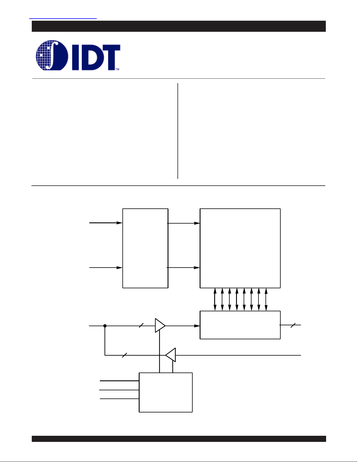
Functional Block Diagram
3.3V CMOS Static RAM
1 Meg (128K x 8-Bit)
Revolutionary Pinout
Description
The IDT71V124 is a 1,048,576-bit high-speed static RAM organized as 128K x 8. It is fabricated using IDT’s high-performance, highreliability CMOS technology. This state-of-the-art technology, combined with innovative circuit design techniques, provides a costeffective solution for high-speed memory needs. The JEDEC center
power/GND pinout reduces noise generation and improves system
performance.
The IDT71V124 has an output enable pin which operates as fast as
7ns, with address access times as fast as 15ns available. All bidirectional inputs and outputs of the IDT71V124 are LVTTL-compatible and
operation is from a single 3.3V supply. Fully static asynchronous
circuitry is used; no clocks or refreshes are required for operation.
The IDT71V124 is packaged in 32-pin 400 mil Plastic SOJ.
IDT71V124
A
I/O0-I/O
A
0
•
•
•
PART IN
ADDRESS
•
•
•
1,048,576-BIT
MEMORY ARRAY
DECODER
16
7
OBSOLESCENCE
8
ORDER 71V124SA
8
FOR NEW DESIGNS
I/OCONTROL
8
WE
OE
CS
CONTROL
LOGIC
©2000 Integrated Device Technology, Inc.
3484 drw01
AUGUST 2000
1
DSC-3484/05

IDT71V124, 3.3V CMOS Static RAM
1 Meg (128K x 8-Bit), Revolutionary Pinout Commercial and Industrial Temperature Ranges
Pin Configuration
Absolute Maximum Ratings
(1)
A
A
A
A
CS
I/O
I/O
V
DD
GND
I/O
I/O
WE
A
A
A
A
0
A
1
2
3
0
1
2
3
4
5
6
7
1
2
3
4
5
6
SO32-3
7
8
9
10
11
12
13 20
14 19
15 18
16
32
31
30
29
28
27
26
25
24
23
22
21
17
SOJ
16
A
15
A
14
A
13
OE
I/O
I/O
GND
V
DD
I/O
I/O
A
12
A
11
A
10
A
9
A
8
3484 drw 02
7
6
5
4
Top View
Truth Table
CS OE WE I/O Function
LLHDATA
LXLDATA
L H H High-Z Output Disabled
H X X High-Z Deselected – St andby (I
(3)
X X High-Z Deselected – Standby (I
V
HC
NOTES:
1. H = VIH, L = VIL, x = Don't care.
2. VLC = 0.2V, VHC = VDD –0.2V.
3. Other inputs ≥VHC or ≤VLC.
(1,2)
OUT
Read Data
IN
Write Dat a
SB
)
PART IN
SB1
3484 tbl 01
Capacitance
(TA = +25°C, f = 1.0MHz, SOJ package)
Symbol Parameter
C
IN
Input Capacitance VIN = 3dV 8 pF
C
I/O
I/O C apacitance V
NOTE:
1. This parameter is guaranteed by device characterization, but is not production
tested.
(1)
OBSOLESCENCE
Conditions Max. Unit
ORDER 71V124SA
OUT
= 3dV 8 pF
3484 tbl 03
FOR NEW DESIGNS
Symbol Rating Value Unit
V
TERM
(2)
Te rm in a l V o lt a ge wi t h
–0.5 to +4. 1
(2)
Respect to GND
T
A
T
BIAS
T
STG
P
T
I
OUT
NOTES:
1. Stresses greater than those listed under ABSOLUTE MAXIMUM RATINGS may
cause permanent damage to the device. This is a stress rating only and functional
operation of the device at these or any other conditions above those indicated in the
operational sections of this specification is not implied. Exposure to absolute
maximum rating conditions for extended periods may affect reliabilty.
2. VTERM must not exceed VDD + 0.5V.
Operating Temperature 0 to +70
Temp e rature Und er B ias –55 to + 125
Storage Temperature –55 to +125
Po we r Di ss i p atio n 0.5 W
DC Output Current 50 mA
Recommended Operating
Temperature and Supply Voltage
Grade Temperature GND V
Commercial 0° C to +70°C 0V Se e B elo w
Indus trial –40°C to +85° C 0V See B e lo w
)
Recommended DC Operating
Conditions
Symbol Parameter Min. Typ. Max. Unit
DD Supp ly Vol tage 3.0 3.3 3.6 V
V
GND Ground 0 0 0 V
V
IH Inp ut Hi g h Vo l tag e 2.0
V
IL Inpu t Lo w Vo l tag e –0. 3
NOTE:
1. VIL (min.) = –1V for pulse width less than 5ns, once per cycle.
____
VDD +0.3 V
(1)
____
V
o
o
o
3484 t bl 02
DD
3484 tbl 02a
0.8 V
3484 tbl 04
C
C
C
DC Electrical Characteristics
(VDD = 3.3V ± 10%, Commercial and Industrial Temperature Ranges)
Symbol Parameter Test Condition
|I
LI| In put Leakage C urrent VDD = Max., VIN = GND to VDD
LO| Output Leakage Current VDD = Max., CS = VIH, VOUT = GND to VDD
|I
V
OL Output Low Voltage IOL = 8mA, VDD = Min.
V
OH Out put H igh Voltage IOH = –8mA, VDD = M in. 2.4
6.42
2
IDT71V124
Min. Max.
___
___
___
5µA
5µA
0.4 V
___
Unit
V
348 4 t bl 0 5
IDT71V124, 3.3V CMOS Static RAM
1 Meg (128K x 8-Bit), Revolutionary Pinout Commercial and Industrial Temperature Ranges
MAX
(1)
(2)
71V124S15 71V124S20
100 120 95 115 mA
DC Electrical Characteristics
(VDD = 3.3V ± 10%, VLC = 0.2V, VHC = VDD – 0.2V)
Symbol Parameter Com'l. Ind. Com'l. Ind. Unit
I
CC
Dyna m ic Ope rating Current
CS <
VIL, Outputs Open, VDD = Max., f = f
SB
I
SB1
I
NOTES:
1. All values are maximum guaranteed values.
2. fMAX = 1/tRC (all address inputs are cycling at fMAX); f = 0 means no address input lines are changing.
Standby Power Sup ply Current (TTL Lev el)
VIH, Outputs Open, VDD = Max., f = f
CS >
Full Standby P ower Sup ply C urrent (CM OS Lev el)
VHC, Outputs Open, VDD = Max., f = 0
CS >
VIN < VLC or VIN > V
HC
MAX
(2)
(2)
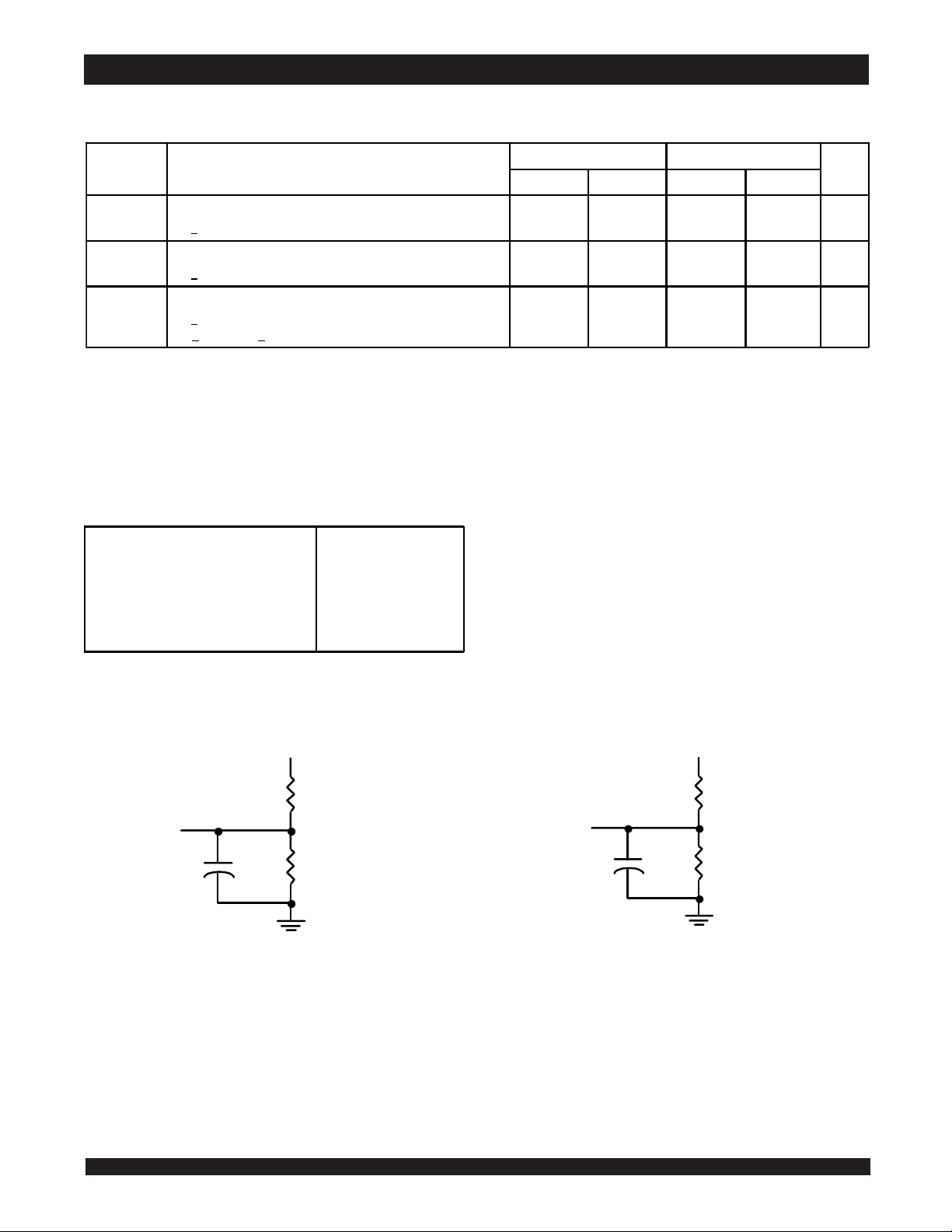
AC Test Conditions
Input Pulse Levels
Input Rise/Fall Times
Input Tim ing Reference Levels
Output R eference Levels
AC Test Load
PART IN
GND t o 3.0V
3ns
1.5V
1.5V
See Figure 1 and 2
3484 tbl 07
35 40 30 35 mA
5757mA
3484 tbl 06
DATA
OUT
3.3V
298Ω
OBSOLESCENCE
ORDER 71V124SA
DATA
OUT
216Ω30pF
3.3V
298Ω
216Ω5pF*
FOR NEW DESIGNS
3484 drw 04
Figure 1. AC Test Load
3484 drw 03
6.42
*Including jig and scope capacitance.
Figure 2. AC Test Load
(for tCLZ, tOLZ, tCHZ, tOHZ, tOW, and tWHZ)
3

IDT71V124, 3.3V CMOS Static RAM
1 Meg (128K x 8-Bit), Revolutionary Pinout Commercial and Industrial Temperature Ranges
AC Electrical Characteristics
(VDD = 3.3V ± 10%, Commercial and Industrial Ranges)
71V124S15 71V124S20
Symbol Parameter Min. Max. Min. Max. Unit
READ CYCLE
RC Re ad Cycl e Time 15
t
t
AA Address Access Time
ACS Chip Select Access Time
t
(1)
CLZ
t
(1)
t
CHZ
OE Output E nabl e to Outp ut Valid
t
(1)
OLZ
t
(1)
t
OHZ
OH Output Hol d fro m Ad dr es s Chang e 4
t
(1)
PU
t
(1)
t
PD
Chi p Se l e c t to Output i n Low-Z 3
Chip Dese lect to Output in High-Z 0 7 0 8 ns
O utp ut E nable to Outp ut i n Low-Z 0
Ou tp ut Dis ab le to O utp ut in Hig h -Z 0 5 0 7 ns
Chip Se l ec t to P o wer-Up Time 0
Chip De s e le c t to P o we r-Do wn Time
____
____
____
____
____
15
15
____
____
____
____
15
20
____
____
3
7
____
0
4
0
____
____
20 ns
20 ns
____
8ns
____
____
____
20 ns
ns
ns
ns
ns
ns
WRIT E C YC L E
WC Write Cycle Time 15
t
tAW Address Valid to End of Write 12
CW Chip Selec t to End of Write 12
t
AS Address Set-up Time 0
t
WP Write Puls e Wid th 12
t
WR Write Recovery Time 0
t
DW Data Valid to End of Write 8
t
PART IN
tDH Data Ho ld Time 0
OW
t
t
WHZ
(1)
(1)
OBSOLESCENCE
O utp ut Ac tiv e from E nd o f Wr ite 3
Wri te Enabl e to Output in Hig h-Z 0 5 0 8 ns
ORDER 71V124SA
FOR NEW DESIGNS
NOTE:
1. This parameter guaranteed with the AC load (Figure 2) by device characterization, but is not production tested.
____
____
____
____
____
____
____
____
____
20
15
15
15
____
____
____
0
0
9
0
4
____
____
____
____
____
____
ns
ns
ns
ns
ns
ns
ns
ns
ns
3484 tbl 08
6.42
4

IDT71V124, 3.3V CMOS Static RAM
1 Meg (128K x 8-Bit), Revolutionary Pinout Commercial and Industrial Temperature Ranges
Timing Waveform of Read Cycle No. 1
ADDRESS
AA
t
OE
(5)
t
t
CLZ
OLZ
t
ACS
(5)
DATA
VCCSUPPLY
CURRENT
CS
OUT
I
I
CC
SB
HIGH IMPEDANCE
t
PU
(1)
t
RC
t
OE
(3)
(5)
t
OHZ
(5)
t
CHZ
DATA
OUT
VALID
t
PD
3484 drw 05
Timing Wav efo rm of Read Cycle No . 2
ADDRESS
PART IN
tOH tOH
DATAOUT
NOTES:
1. WE is HIGH for Read Cycle.
2. Device is continuously selected, CS is LOW.
3. Address must be valid prior to or coincident with the later of CS transition LOW; otherwise tAA is the limiting parameter.
4. OE is LOW.
5. Transition is measured ±200mV from steady state.
OBSOLESCENCE
ORDER 71V124SA
tAA
(1,2,4)
tRC
FOR NEW DESIGNS
DATAOUT VALIDPREVIOUS DATAOUT VALID
3484 drw 06
6.42
5

IDT71V124, 3.3V CMOS Static RAM
7
1 Meg (128K x 8-Bit), Revolutionary Pinout Commercial and Industrial Temperature Ranges
Timing Wav eform of Write Cycle No.1 (WE Controlled Timing)
WC
t
ADDRESS
t
AW
CS
t
WR
(5)
t
OW
t
DH
DATA
DATA
WE
OUT
t
AS
(5)
t
WHZ
IN
(2)
t
WP
HIGH IMPEDANCE
t
DW
DATAINVALID
(1,2,4)
(3)(3)
t
CHZ
(5)
3484 drw0
Timing Wav eform of Write Cycle No. 2 (CS Controlled Timing)
t
t
AW
t
WC
CW
t
DW
DATAINVALID
t
WR
(3)
t
DH
ADDRESS
CS
WE
DATA
PART IN
t
AS
OBSOLESCENCE
IN
ORDER 71V124SA
FOR NEW DESIGNS
NOTES:
1. A write occurs during the overlap of a LOW CS and a LOW WE.
2. OE is continuously HIGH. During a WE controlled write cycle with OE LOW, tWP must be greater than or equal to tWHZ + tDW to allow the I/O drivers to turn off and data to be
placed on the bus for the required tDW. If OE is HIGH during a WE controlled write cycle, this requirement does not apply and the minimum write pulse is the specified tWP.
3. During this period, I/O pins are in the output state, and input signals must not be applied.
4. If the CS LOW transition occurs simultaneously with or after the WE LOW transition, the outputs remain in a high impedance state. CS must be active during the tCW write
period.
5. Transition is measured ±200mV from steady state.
(1,4)
3484 drw 08
6.42
6

IDT71V124, 3.3V CMOS Static RAM
T
1 Meg (128K x 8-Bit), Revolutionary Pinout Commercial and Industrial Temperature Ranges
Ordering Information
ID
71V124
Device
Type
S
PowerXXSpeedXPackage
X
Process/
Temperature
Range
Blank
I
Y400-milSOJ(SO32-3)
15
20
Commerc ial (0°C to +70°C)
Industrial (-40°C to +85°C)
Speed in nanoseconds
3484 drw 09
PART IN
OBSOLESCENCE
ORDER 71V124SA
FOR NEW DESIGNS
6.42
7

IDT71V124, 3.3V CMOS Static RAM
1 Meg (128K x 8-Bit), Revolutionary Pinout Commercial and Industrial Temperature Ranges
Datasheet Document History
11/1/99 Updated to new format
Pg. 2 Expressed commercial and industrial temperature ranges on DC Electrical table
Pg. 2 Added Recommended Operating Temperature and Supply Voltage table
Pg. 4 Expressed commercial and industrial ranges on AC Electrical table
Pg. 4 Revised footnotes and notes on AC Electrical table
Pg. 6 Revised footnotes on Write Cycle No. 1 diagram
Pg. 8 Added datasheet document history
08/30/00 Part in obsolescence; order part 71V124SA. See PDN# S-0004
PART IN
OBSOLESCENCE
CORPORATE HEADQUARTERS for SALES: for Tech Support:
2975 Stender Way 800-345-7015 or 408-727-6116 sramhelp@idt.com
Santa Clara, CA 95054 fax: 408-492-8674 800-544-7726, x4033
ORDER 71V124SA
FOR NEW DESIGNS
www.idt.com
The IDT logo is a registered trademark of Integrated Device Technology, Inc.
8
 Loading...