Datasheet IDT71V016SA10BF8, IDT71V016SA10PH8, IDT71V016SA10Y8, IDT71V016SA12BF8, IDT71V016SA12BFI8 Datasheet (Integrated Device Technology Inc)
...Page 1

3.3V CMOS Static RAM
1 Meg (64K x 16-Bit)
IDT71V016SA
Features
◆◆
◆
◆◆
64K x 16 advanced high-speed CMOS Static RAM
◆◆
◆
◆◆
Equal access and cycle times
— Commercial: 10/12/15/20ns
— Industrial: 12/15/20ns
◆◆
◆
◆◆
One Chip Select plus one Output Enable pin
◆◆
◆
◆◆
Bidirectional data inputs and outputs directly
LVTTL-compatible
◆◆
◆
◆◆
Low power consumption via chip deselect
◆◆
◆
◆◆
Upper and Lower Byte Enable Pins
◆◆
◆
◆◆
Single 3.3V power supply
◆◆
◆
◆◆
Available in 44-pin Plastic SOJ, 44-pin TSOP, and
48-Ball Plastic FBGA packages
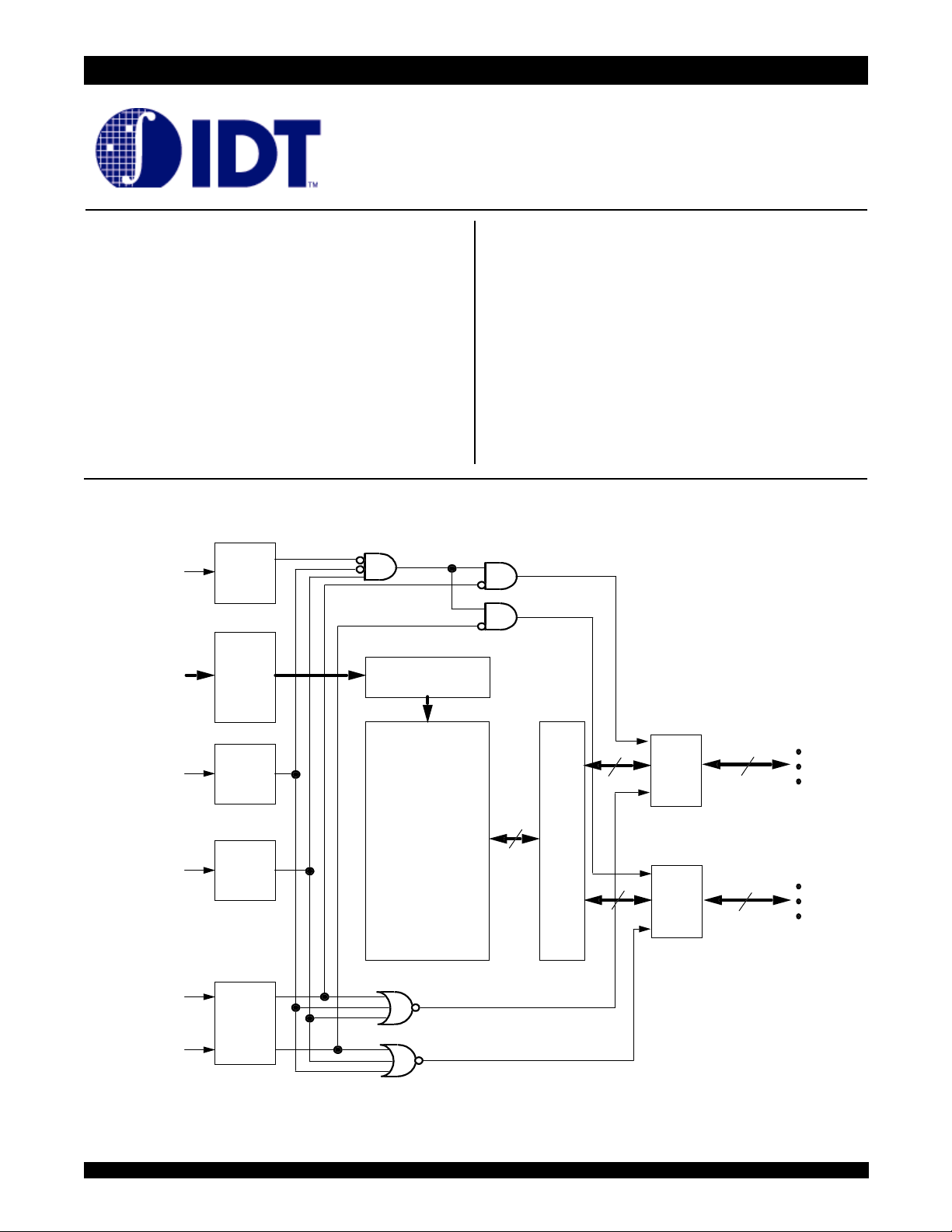
Functional Block Diagram
Output
Enable
Buffer
Address
Buffers
A0–A
OE
15
Row / Column
Decoders
Description
The IDT71V016 is a 1,048,576-bit high-speed Static RAM organized
as 64K x 16. It is fabricated using IDT’s high-perfomance, high-reliability
CMOS technology. This state-of-the-art technology, combined with innovative circuit design techniques, provides a cost-effective solution for highspeed memory needs.
The IDT71V016 has an output enable pin which operates as fast
as 5ns, with address access times as fast as 10ns. All bidirectional
inputs and outputs of the IDT71V016 are LVTTL-compatible and operation
is from a single 3.3V supply. Fully static asynchronous circuitry is used,
requiring no clocks or refresh for operation.
The IDT71V016 is packaged in a JEDEC standard 44-pin Plastic
SOJ, a 44-pin TSOP Type II, and a 48-ball plastic 7 x 7 mm FBGA.
CS
WE
BHE
BLE
©2000 Integrated Device Technology, Inc.
Chip
Enable
Buffer
Write
Enable
Buffer
Byte
Enable
Buffers
64K x 16
Memory
Array
I/O
15
8
Sense
16
Amps
and
Write
Drivers
8
High
Byte
I/O
Buffer
Low
Byte
I/O
Buffer
8
8
3834 drw01
I/O
I/O
I/O
8
7
0
JUNE 2002
1
DSC-3834/06
Page 2

IDT71V016SA, 3.3V CMOS Static RAM
I/O0-I/O7I/O8-I/O15Function
1 Meg (64K x 16-Bit) Commercial and Industrial Temperature Ranges
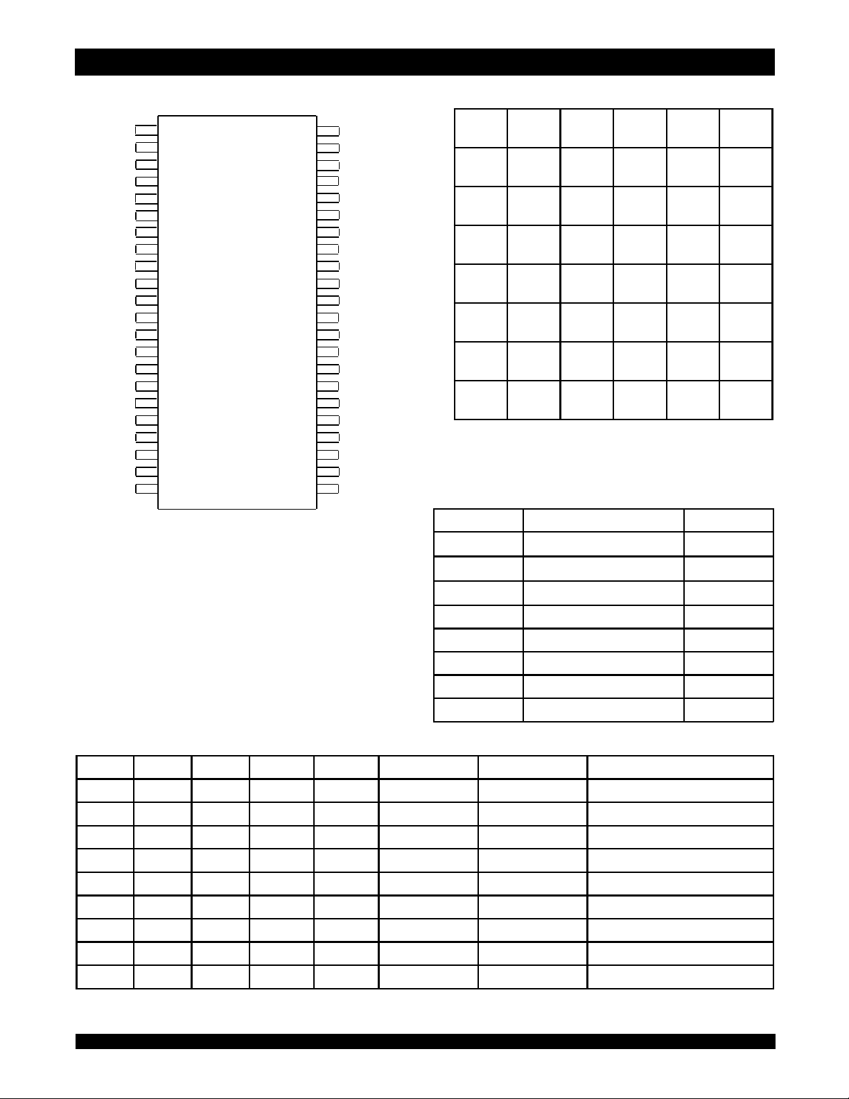
Pin Configurations
1
4
2
3
3
2
1
4
0
5
6
7
0
8
1
2
9
3
10
11
12
4
13
5
14
6
15
7
16
SO44-1
SO44-2
17
18
19
20
21
22
I/O
I/O
I/O
I/O
V
V
I/O
I/O
I/O
I/O
WE
A
A
A
A
A
A
A
A
A
CS
DD
SS
15
14
13
12
NC
44
43
42
41
40
39
38
37
36
35
34
33
32
31
30
29
28
27
26
25
24
23
A
5
A
6
A
7
OE
BHE
BLE
I/O
I/O
I/O
I/O
V
SS
V
DD
I/O
I/O
I/O
I/O
NC
A
8
A
9
A
10
A
11
NC
123456
A
BLE OE
BI/O
CI/O9I/O
15
14
13
12
DVSSI/O
EVDDI/O
FI/O14I/O
11
10
9
8
GI/O15NC A
8
BHE
10
11
12
13
HNC A8A
A
0
3
A
A
5
NC A
A
1
4
A
A
6
7
NC NC I/O
14
A
12
9
15
A
13
A
10
A
FBGA (BF48-1)
A
CS
I/O
I/O
I/O
WE
A
1
3
4
5
NC
0
I/O
I/O
2
DD
V
SS
V
6
I/O
7
I/O
NC
3834 tbl 02a
2
11
Top View
Pin Description
15
SOJ/TSOP
Top View
3834 drw 02
A0 – A
CS
WE
OE
Address Inputs Input
Chip Select Input
Write Enable Input
Output En able Input
BHE High By te Enable Input
BLE Low By te En able Input
0
15
Truth Table
(1)
I/O
V
V
– I/O
DD
SS
Data Input/Output I/O
3.3V Pow er Pow er
Ground Gnd
CS OE WE BLE BHE
H X X X X High-Z High-Z Deselected – Stan dby
LLHL H DATA
L L H H L High-Z DATA
LLHL L DATA
LXL L L DATA
LXL L H DATA
L X L H L High-Z DATA
OUT
OUT
High-Z Low By t e Read
OUT
OUT
DATA
IN
IN
IN
DATA
High-Z Low By t e Write
IN
High Byt e Read
Word Re ad
Word Write
High Byt e Write
L H H X X H igh-Z High-Z Outputs D isabled
L X X H H H igh-Z High-Z Outputs D isabled
NOTE:
1. H = VIH, L = VIL, X = Don't care.
3834 tbl 01
3834 tbl 02
6.42
2
Page 3

IDT71V016SA, 3.3V CMOS Static RAM
Symbol
Parameter
71V016SA10
71V016SA12
71V016SA15
71V016SA20
Unit
Com'l Only
Com'l
Ind
Com'l
Ind
Com'l
Ind
Max.
Typ.
(4)
Symbol
Rating
Value
Unit
Grade
Temperature
VSSV
DD
Symbol
Parameter
Min.
Typ.
Max.
Unit
(1 )
___
___
___
___
1 Meg (64K x 16-Bit) Commercial and Industrial Temperature Ranges
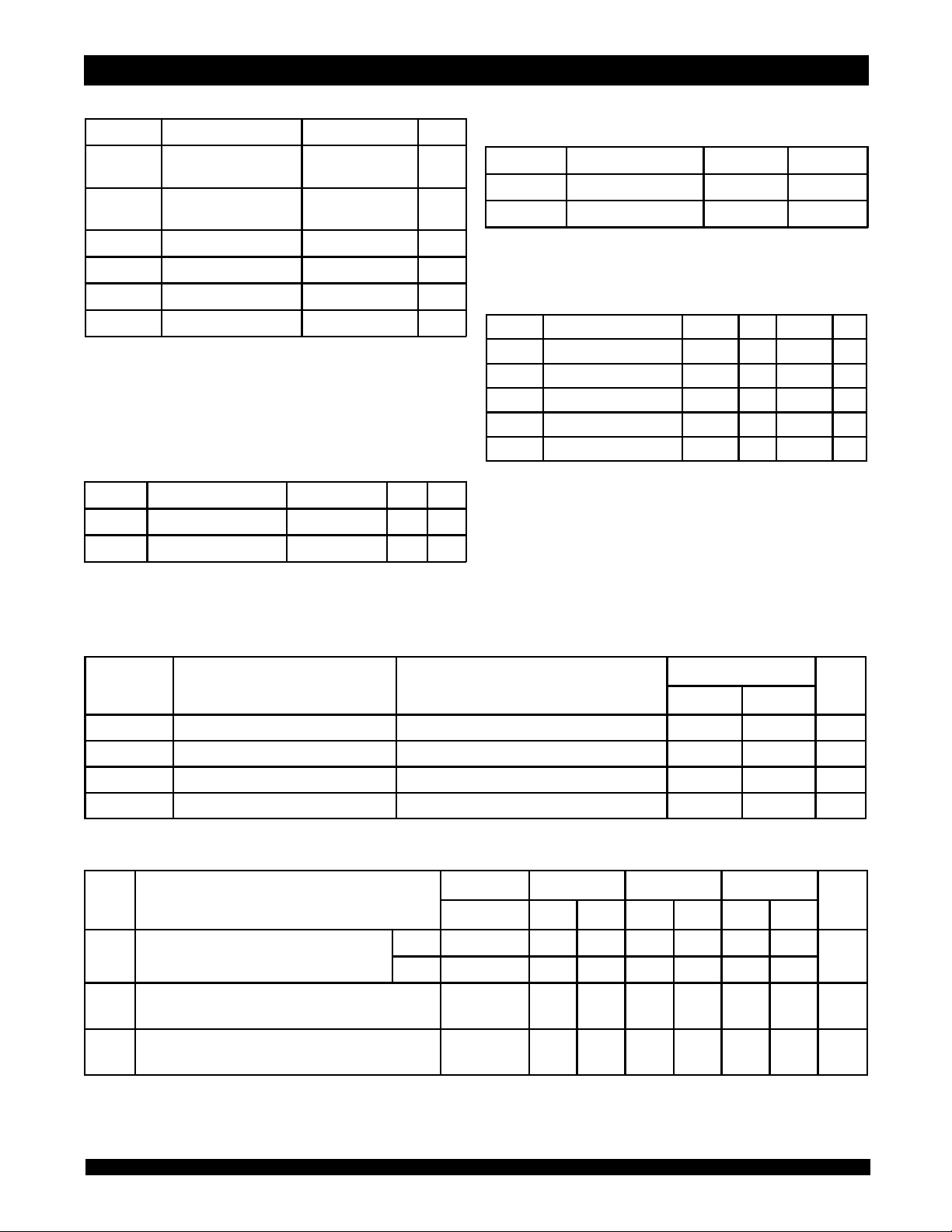
Absolute Maximum Ratings
(1)
Recommended Operating
Temperature and Supply Voltage
DD
V
IN
, V
V
BIAS
T
STG
T
T
P
OUT
I
NOTE:
1. Stresses greater than those listed under ABSOLUTE MAXIMUM RATINGS may cause
permanent damage to the device. This is a stress rating only and functional operation
of the device at these or any other conditions above those indicated in the operational
sections of this specification is not implied. Exposure to absolute maximum rating
conditions for extended periods may affect reliability.
Capacitance
(TA = +25°C, f = 1.0MHz, SOJ package)
Symbol Parameter
C
IN
C
I/O
NOTE:
1. This parameter is guaranteed by device characterization, but not production tested.
Supply Voltage Relativ e to
SS
V
Terminal Voltage Relative
OUT
SS
to V
–0.5 t o +4. 6 V
–0.5 t o VDD+0.5 V
Tem perature Under Bias –55 to +125
Storage Temperature –55 to + 125
Pow er Dissipation 1.25 W
DC Out put C urrent 50 mA
Con ditio ns M ax. Unit
Input Capacitance VIN = 3dV 6 pF
I/O C apacitance V
= 3dV 7 pF
OUT
o
C
o
C
3834 tbl 03
3834 tbl 0 6
Com me rc ial 0° C to +7 0°C 0V Se e Be lo w
Indus trial -40° C to + 85°C 0V Se e B e lo w
Recommended DC Operating
Conditions
(1)
V
Supply Voltage 3.15 3.3 3.6 V
DD
(2)
DD
V
Supply Voltage 3.0 3.3 3.6 V
Vss Ground 0 0 0 V
IH
V
Input H igh Voltage 2.0
IL
V
Input L ow Voltage –0.3
NOTES:
1. For 71V016SA10 only.
2. For all speed grades except 71V016SA10.
3. VIH (max.) = VDD+2V for pulse width less than 5ns, once per cycle.
4. VIL (min.) = –2V for pulse width less than 5ns, once per cycle.
____
VDD+0.3
(4 )
____
0.8 V
3834 tbl 04
(3)
3834 tbl 05
V
DC Electrical Characteristics
(VDD = Min. to Max., Commercial and Industrial Temperature Ranges)
Symbol Parameter Test Condition
LI
|I
| Input Leakage C urrent VDD = Max., VIN = VSS to V
LO
|I
| O utput Leakage Current VDD = Max., CS = VIH, V
OL
V
OH
V
DC Electrical Characteristics
Output Low Voltage IOL = 8mA, VDD = Min.
Output H igh Voltage IOH = –4mA, VDD = M in. 2.4
(1,2)
(VDD = Min. to Max., VLC = 0.2V, VHC = VDD – 0.2V)
Dynamic Operating Current
CC
I
LC
CS ≤ V
Dynamic Standby Power Supply Current
SB
I
CS ≥ V
Full Stand b y Po we r Sup p ly Current (static )
SB1
I
CS ≥ V
, Outputs Open, VDD = Max., f = f
HC
, Outputs Open, VDD = Max., f = f
HC
, Outputs Open, VDD = Max., f = 0
MAX
MAX
(3)
(3)
(3)
NOTES:
1. All values are maximum guaranteed values.
2. All inputs switch between 0.2V (Low) and VDD – 0.2V (High).
3. fMAX = 1/tRC (all address inputs are cycling at fMAX); f = 0 means no address input lines are changing .
4. Typical values are measured at 3.3V, 25°C and with equal read and write cycles.
6.42
160 150 160 130 130 120 120
125 120 -- 110 -- 110 --
45 40 45 35 35 30 30
10 10 10 10 10 10 10 mA
3
DD
OUT
= VSS to V
IDT71V016SA
UnitMin. Max.
5µA
DD
5µA
0.4 V
V
3834 tbl 0 7
mA
mA
3834 tbl 08
Page 4

IDT71V016SA, 3.3V CMOS Static RAM
1 Meg (64K x 16-Bit) Commercial and Industrial Temperature Ranges
AC Test Conditions
Input Pulse Lev els
Input Rise/Fall Times
Input Tim ing Refere nce Leve ls
Output Reference Lev els
AC Test Load
AC Test Loads
=50
Z
I/O
0
Figure 1. AC Test Load
GND to 3.0V
1.5ns
1.5V
1.5V
See Figure 1, 2 and 3
3834 tbl 09
3.3V
+1.5V
Ω
50
Ω
30pF
3834 drw 03
DATA
OUT
5pF*
*Including jig and scope capacitance.
320
350
Ω
Ω
3834 drw 04
Figure 2. AC Test Load
(for tCLZ, tOLZ, tCHZ, tOHZ, tOW, and tWHZ)
AA,tACS
∆
t
(Typical, ns)
7
6
5
4
3
2
1
·
8
•
•
•
20 40 60 80 100 120 140 160
•
•
CAPACITANCE(pF)
Figure 3. Output Capacitive Derating
180
3834 drw 05
•
200
6.42
4
Page 5

IDT71V016SA, 3.3V CMOS Static RAM
71V016S A10
(2)
71V016S A12
71V016S A15
71V016S A20
Symbol
Parameter
Min.
Max.
Min.
Max.
Min.
Max.
Min.
Max.
Unit
READ CYCL E
WRITE CYCLE
1 Meg (64K x 16-Bit) Commercial and Industrial Temperature Ranges
AC Electrical Characteristics (VDD = Min. to Max., Commercial and Industrial Temperature Ranges)
t
t
t
t
t
t
t
t
t
t
t
t
t
t
t
t
t
t
t
t
t
t
t
RC
AA
ACS
CLZ
CHZ
OE
OLZ
OHZ
OH
BE
BLZ
BHZ
WC
AW
CW
BW
AS
WR
WP
DW
DH
OW
WHZ
Re ad Cyc l e Time 10
Address Access Time
Chip Select Access Time
(1)
(1)
Chip S el e ct Low to Outp ut in Low- Z 4
Chip Select High to Output in High-Z
Output Enab l e L o w to O utp ut Va li d
(1)
(1)
Output E nab le Low to Output i n Lo w-Z 0
Outp u t E nab l e Hig h to Ou tp ut i n Hi g h- Z
____
____
____
____
____
____
____
____
12
10
10
____
____
4
5
5
____
____
0
5
____
Output Hold from Address Change 4 — 4 — 4 — 4 — ns
Byte En ab l e Lo w to Output Vali d — 5 — 6 — 7
(1)
(1)
By te E nab le Low to Output i n Low-Z 0
By te E nab le High to Output i n Hig h-Z
____
Write Cycle Time 10
Address Valid to End of Write 7
Chip Sele ct Low to End of Write 7
By te Enab le Lo w to E nd o f Write 7
Address Set-up Time 0
Address Hold from End of Write 0
Write Pulse Width 7
Data Vali d to En d of Write 5
Data Ho ld Tim e 0
(1)
(1)
Write Enable High to Output in Low-Z 3
Write E nab le Low to Output i n Hig h-Z
____
____
____
____
____
____
____
____
____
____
____
____
0
5
____
12
8
8
8
0
0
8
6
0
3
5
____
____
____
____
____
____
____
____
____
____
____
____
____
____
____
15
12
12
____
____
5
____
6
____
6
0
____
6
0
____
6
15
10
10
10
0
0
10
7
0
3
____
6
NOTES:
1. This parameter is guaranteed with the AC Load (Figure 2) by device characterization, but is not production tested.
2. 0°C to +70°C temperature range only.
____
____
____
____
____
____
____
____
____
____
____
____
____
____
20
15
15
____
____
5
6
7
____
____
0
6
____
____
0
6
____
20
12
12
12
0
0
12
9
0
3
6
____
____
ns
20 ns
20 ns
____
ns
8ns
8ns
____
ns
8ns
8ns
____
ns
8ns
____
____
____
____
____
____
____
____
____
____
ns
ns
ns
ns
ns
ns
ns
ns
ns
ns
8ns
3834 tbl 10
Timing Waveform of Read Cycle No. 1
t
RC
ADDRESS
t
AA
t
OH
DATA
OUT
NOTES:
1. WE is HIGH for Read Cycle.
2. Device is continuously selected, CS is LOW.
3. OE, BHE , and BLE are LOW.
PREVIOUS DATA
OUT
VALID
6.42
5
(1,2,3)
DATA
OUT
VALID
t
OH
3834 drw 06
Page 6

IDT71V016SA, 3.3V CMOS Static RAM
1 Meg (64K x 16-Bit) Commercial and Industrial Temperature Ranges
Timing Waveform of Read Cycle No. 2
t
(1)
RC
ADDRESS
t
AA
OE
t
OE
(3)
t
OLZ
CS
(2)
t
ACS
(3)
t
CLZ
BLE
BHE,
(2)
t
BE
(3)
t
BLZ
DATA
OUT
DATA VALID
OUT
NOTES:
1. WE is HIGH for Read Cycle.
2. Address must be valid prior to or coincident with the later of CS, BHE, or BLE transition LOW; otherwise tAA is the limiting parameter.
3. Transition is measured ±200mV from steady state.
t
OH
(3)
t
OHZ
(3)
t
CHZ
(3)
t
BHZ
3834 drw 07
Timing Waveform of Write Cycle No. 1 (WE Controlled Timing)
WC
t
(1,2,4)
ADDRESS
t
AW
CS
BHE,BLE
WE
DATA
OUT
DATA
t
AS
t
PREVIO USDA T AVAL I D DATAVALID
IN
(3)
WHZ
t
(5)
CW
(2)
t
BW
t
WR
t
WP
(5)
t
OW
t
t
DW
DH
t
CHZ
t
BHZ
(5)
(5)
DATAINVALID
3834 drw 08
NOTES:
1. A write occurs during the overlap of a LOW CS, LOW BHE or BLE, and a LOW WE.
2. OE is continuously HIGH. If during a WE controlled write cycle OE is LOW, tWP must be greater than or equal to tWHZ + tDW to allow the I/O drivers to turn off and data to be placed
on the bus for the required tDW. If OE is HIGH during a WE controlled write cycle, this requirement does not apply and the minimum write pulse is as short as the specified tWP.
3. During this period, I/O pins are in the output state, and input signals must not be applied.
4. If the CS LOW or BHE and BLE LOW transition occurs simultaneously with or after the WE LOW transition, the outputs remain in a high-impedance state.
5. Transition is measured ±200mV from steady state.
6.42
6
Page 7

IDT71V016SA, 3.3V CMOS Static RAM
1 Meg (64K x 16-Bit) Commercial and Industrial Temperature Ranges
Timing Waveform of Write Cycle No. 2 (CS Controlled Timing)
WC
t
ADDRESS
t
AW
CS
t
BW
(2)
t
CW
t
WR
t
t
DW
DH
DATAINVALID
BHE, BLE
OUT
DATA
DATA
WE
t
AS
t
WP
IN
(1,4)
3834 drw 09
Timing Waveform of Write Cycle No. 3 (BHE, BLE Controlled Timing)
t
WC
(1,4)
ADDRESS
t
AW
CS
(2)
t
t
AS
CW
t
BW
BHE, BLE
t
WP
t
WR
WE
DATA
OUT
t
DH
3834 drw 10
DATA
DW
t
IN
DATAINVALID
NOTES:
1. A write occurs during the overlap of a LOW CS, LOW BHE or BLE, and a LOW WE.
2. OE is continuously HIGH. If during a WE controlled write cycle OE is LOW, tWP must be greater than or equal to tWHZ + tDW to allow the I/O drivers to turn off and data to be placed
on the bus for the required tDW. If OE is HIGH during a WE controlled write cycle, this requirement does not apply and the minimum write pulse is as short as the specified tWP.
3. During this period, I/O pins are in the output state, and input signals must not be applied.
4. If the CS LOW or BHE and BLE LOW transition occurs simultaneously with or after the WE LOW transition, the outputs remain in a high-impedance state.
5. Transition is measured ±200mV from steady state.
6.42
7
Page 8

IDT71V016SA, 3.3V CMOS Static RAM
1 Meg (64K x 16-Bit) Commercial and Industrial Temperature Ranges
Ordering Information
IDT
71V016
Device
Type
SA
PowerXXSpeed
XXX
PackageXProcess/
Temperature
Range
X
Tape & Reel
8
Blank
I
Y
PH
BF
Commercial (0°C to +70°C)
Industrial (-40°C to +85°C)
400-mil SOJ (SO44-1)
400-mil TSOP Type II (SO44-2)
7.0 x 7.0 mm FBGA (BF48-1)
10**
12
15
Speed in nanoseconds
20
** Commercial temperature rangeonly.
3834 drw11
6.42
8
Page 9

IDT71V016SA, 3.3V CMOS Static RAM
1 Meg (64K x 16-bit) Commercial and Industrial Temperature Ranges
Datasheet Document History
1/7/00 Updated to new format
Pp. 1, 3, 5, 8 Added Industrial Temperature range offerings
Pg. 2 Numbered I/Os and address pins on FBGA Top View
Pg. 6 Revised footnotes on Write Cycle No. 1 diagram
Pg. 7 Revised footnotes on Write Cycle No. 2 and No. 3 diagrams
Pg. 9 Added Datasheet Document History
08/30/00 Pg. 3 Tighten ICC and ISB.
Pg. 5 Tighten tCLZ, tCHZ, tOHZ, tBHZ and tWHZ
08/22/01 Pg. 8 Removed footnote "available in 15ns and 20ns only"
06/20/02 Pg. 8 Added tape and reel field to ordering information
CORPORATE HEADQUARTERS for SALES: for Tech Support:
2975 Stender Way 800-345-7015 or 408-727-6116 sramhelp@idt.com
Santa Clara, CA 95054 fax: 408-492-8674 800-544-7726, x4033
www.idt.com
The IDT logo is a registered trademark of Integrated Device Technology, Inc.
9
 Loading...