

Page 1
W
查询IDT7203L120D供应商
CMOS ASYNCHRONOUS FIFO
2048 x 9, 4096 x 9,
8192 x 9 and 16384 x 9
Integrated Device Technology, Inc.
FEATURES:
• First-In/First-Out Dual-Port memory
• 2048 x 9 organization (IDT7203)
• 4096 x 9 organization (IDT7204)
• 8192 x 9 organization (IDT7205)
• 16384 x 9 organization (IDT7206)
• High-speed: 12ns access time
• Low power consumption
— Active: 770mW (max.)
— Power-down: 44mW (max.)
• Asynchronous and simultaneous read and write
• Fully expandable in both word depth and width
• Pin and functionally compatible with IDT720X family
• Status Flags: Empty, Half-Full, Full
• Retransmit capability
• High-performance CMOS technology
• Military product compliant to MIL-STD-883, Class B
• Standard Military Drawing for #5962-88669 (IDT7203),
5962-89567 (IDT7203), and 5962-89568 (IDT7204) are
listed on this function
• Industrial temperature range (-40
able, tested to military electrical specifications
.
o
C to +85oC) is avail-
IDT7203
IDT7204
IDT7205
IDT7206
DESCRIPTION:
The IDT7203/7204/7205/7206 are dual-port memory buffers with internal pointers that load and empty data on a firstin/first-out basis. The device uses Full and Empty flags to
prevent data overflow and underflow and expansion logic to
allow for unlimited expansion capability in both word size and
depth.
Data is toggled in and out of the device through the use of
the Write (W) and Read (R) pins.
The devices 9-bit width provides a bit for a control or parity
at the user’s option. It also features a Retransmit (RT) capability that allows the read pointer to be reset to its initial position
when RT is pulsed LOW. A Half-Full Flag is available in the
single device and width expansion modes.
The IDT7203/7204/7205/7206 are fabricated using IDT’s
high-speed CMOS technology. They are designed for applications requiring asynchronous and simultaneous read/writes
in multiprocessing, rate buffering, and other applications.
Military grade product is manufactured in compliance with
the latest revision of MIL-STD-883, Class B.
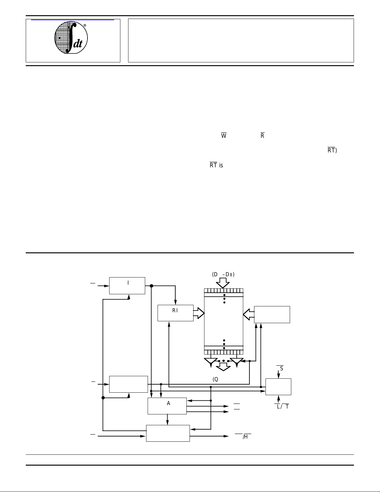
FUNCTIONAL BLOCK DIAGRAM
DATA INPUTS
0(D –D8)
WRITE
CONTROL
WRITE
POINTER
THREESTATE
BUFFERS
R
XI
READ
CONTROL
FLAG
LOGIC
EXPANSION
LOGIC
RAM ARRAY
2048 x 9
4096 x 9
8192 x 9
16384 x 9
DATA OUTPUTS
0(Q –Q8)
EF
FF
XO/HF
READ
POINTER
RS
RESET
LOGIC
FL/RT
2661 drw 01
The IDT logo is a registered trademark of Integrated Device Techology, Inc.
MILITARY AND COMMERCIAL TEMPERATURE RANGES DECEMBER 1996
1996 Integrated Device Technology, Inc. DSC-2661/9
For latest information contact IDT's web site at www.idt.com or fax-on-demand at 408-492-8391.
5.04 1
Page 2
IDT7203/7204/7205/7206 CMOS ASYNCHRONOUS FIFO
2048 x 9, 4096 x 9, 8192 x 9 and 16384 x 9 MILITARY AND COMMERCIAL TEMPERATURE RANGES
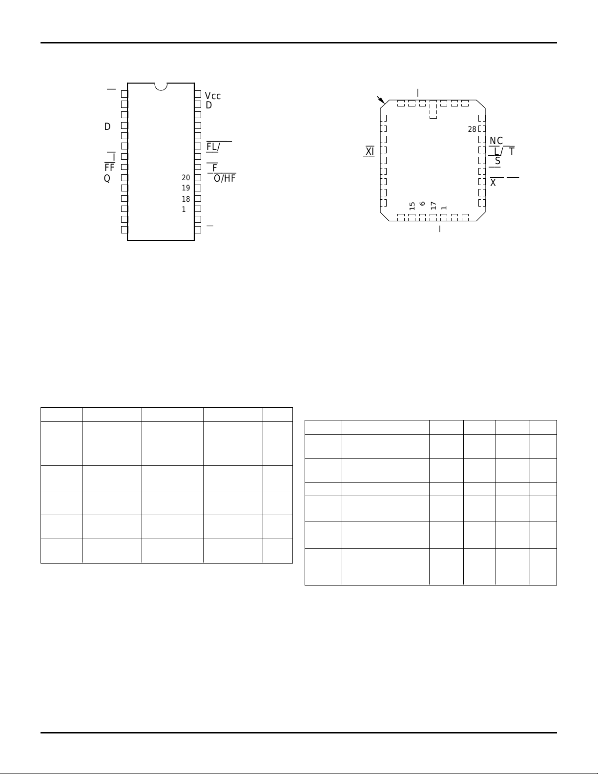
PIN CONFIGURATIONS
W
D
D
D
D
D
XI
FF
Q
Q
Q
Q
Q
GND
1
2
8
3
3
4
2
1
0
0
1
2
3
8
5
6
7
8
9
10
11
12
13
14
P28-1
P28-2
D28-1
D28-3
SO28-3
28
27
26
25
24
23
22
21
20
19
18
17
16
15
2661 drw 02a
Vcc
D
4
D
5
6
D
D
7
FL/RT
RS
EF
XO/HF
Q
7
6
Q
5
Q
Q
4
R
DIP
TOP VIEW
NOTES:
1. The THINDIPs P28-2 and D28-3 are only available for the 7203/7204/
7205.
2. The small outline package SO28-3 is only available for the 7204.
3. Consult factory for CERPACK pinout.
INDEX
2
D
D
1
0
D
XI
FF
Q
0
1
Q
NC
Q
2
8
D3D
432
5
6
7
8
9
10
11
12
13
1415161718
3
8
Q
Q
PLCC/LCC
TOP VIEW
NC
W
1
J32-1
&
L32-1
GND
NC
Vcc
32
R
4
D
31
19
Q
4
5
D
30
29
28
27
26
25
24
23
22
21
20
5
Q
2661 drw 02b
D
6
D
7
NC
FL/RT
RS
EF
XO/HF
Q
7
Q
6
ABSOLUTE MAXIMUM RATINGS
(1)
Symbol Rating Commercial Military Unit
V
TERM Terminal –0.5 to + 7.0 –0.5 to +7.0 V
Voltage with
Respect to
GND
T
A Operating 0 to +70 –55 to +125 ° C
Temperature
T
BIAS Temperature –55 to +125 –65 to +135 ° C
Under Bias
T
STG Storage –55 to + 125 –65 to +155 ° C
Temperature
I
OUT DC Output 50 50 mA
Current
NOTE: 2661 tbl 01
1. Stresses greater than those listed under ABSOLUTE MAXIMUM RATINGS may cause permanent damage to the device. This is a stress rating
only and functional operation of the device at these or any other conditions
above those indicated in the operational sections of this specification is not
implied. Exposure to absolute maximum rating conditions for extended
periods may affect reliability.
RECOMMENDED DC OPERATING
CONDITIONS
Symbol Parameter Min. Typ. Max. Unit
V
CCM Military Supply 4.5 5.0 5.5 V
Voltage
CCC Commercial Supply 4.5 5.0 5.5 V
V
Voltage
GND Supply Voltage 0 0 0 V
(1)
V
IH
V
IH
V
IL
NOTE: 2661 tbl 02
1. 1.5V undershoots are allowed for 10ns once per cycle.
Input High Voltage 2.0 — — V
Commercial
(1)
Input High Voltage 2.2 — — V
Military
(1)
Input Low Voltage — — 0.8 V
Commercial and
Military
5.04 2
Page 3
IDT7203/7204/7205/7206 CMOS ASYNCHRONOUS FIFO
2048 x 9, 4096 x 9, 8192 x 9 and 16384 x 9 MILITARY AND COMMERCIAL TEMPERATURE RANGES
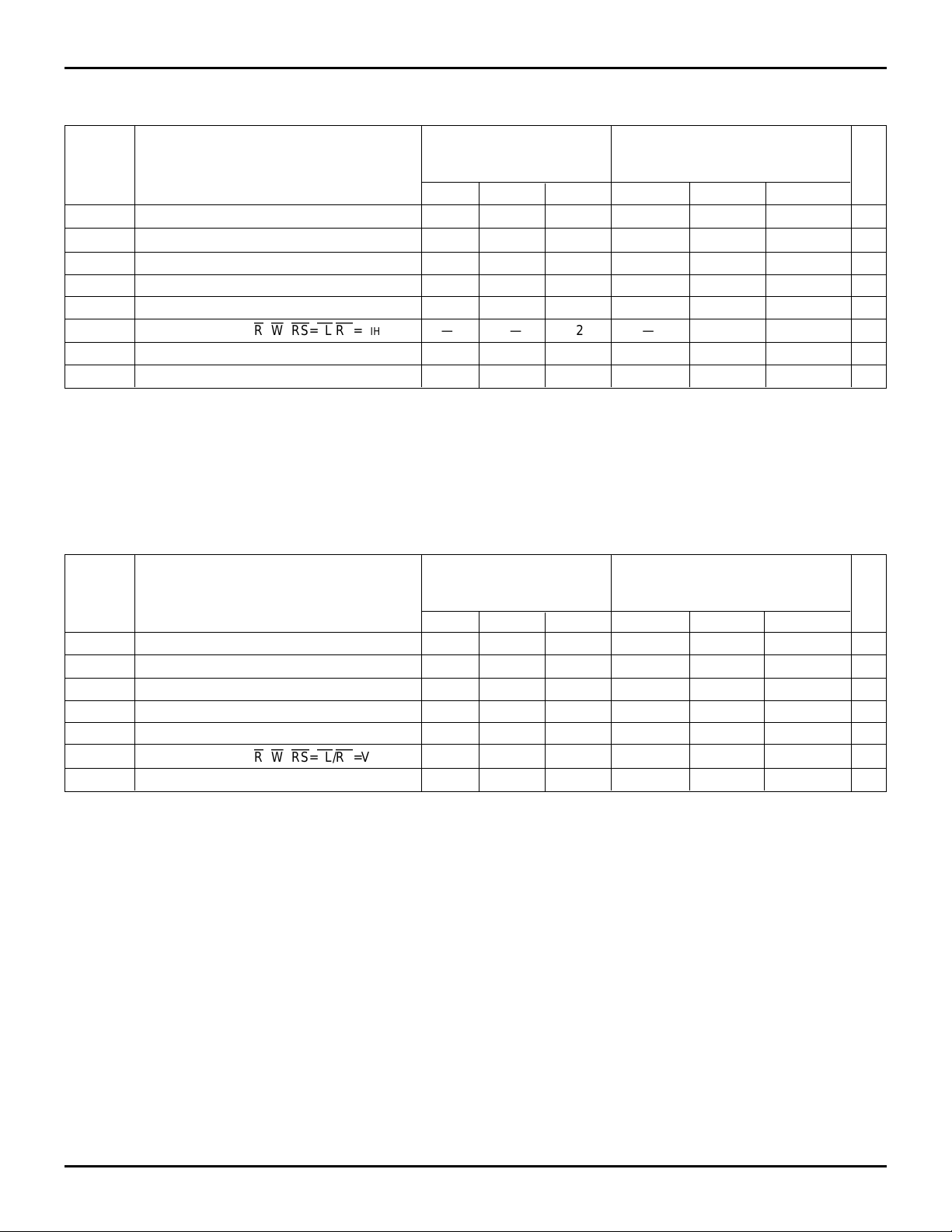
DC ELECTRICAL CHARACTERISTICS FOR THE 7203 AND 7204
(Commercial: VCC = 5.0V±10%, TA = 0°C to +70°C; Military: VCC = 5.0V±10%, TA = –55°C to +125°C)
IDT7203/7204 IDT7203/7204
Commercial Military
tA = 12, 15, 20, 25, 35, 50 ns tA = 20, 30, 40, 50, 65, 80, 120 ns
Symbol Parameter Min. Typ. Max. Min. Typ. Max. Unit
(2)
LI
I
(3)
LO
I
OH Output Logic “1” Voltage IOH = –2mA 2.4 — — 2.4 — — V
V
OL Output Logic “0” Voltage IOL = 8mA — — 0.4 — — 0.4 V
V
(4)
CC1
I
(4)
CC2
I
CC3(L)
I
CC3(S)
I
NOTES: 2661 tbl 03
1. Speed grades 65, 80, and 120ns are only available in the ceramic DIP.
2. Measurements with 0.4 ≤ V
3. R ≥ V
CC measurements are made with outputs open (only capacitive loading).
4. I
5. Tested at f = 20MHz.
Input Leakage Current (Any Input) –1 — 1 –1 — 1 µA
Output Leakage Current –10 — 10 –10 — 10 µA
Active Power Supply Current — — 120
(5)
— — 150
Standby Current (R=W=RS=FL/RT=VIH)——12— —25mA
(4)
Power Down Current (All Input = VCC - 0.2V) — — 2 — — 4 mA
(4)
Power Down Current (All Input = VCC - 0.2V) — — 8 — — 12 mA
IH, 0.4 ≤ VOUT ≤ VCC.
IN ≤ VCC.
(1)
(5)
mA
DC ELECTRICAL CHARACTERISTICS FOR THE 7205 AND 7206
(Commercial: VCC = 5.0V±10%, TA = 0°C to +70°C; Military: VCC = 5.0V±10%, TA = –55°C to +125°C)
IDT7205/7206 IDT7205/7206
Commercial Military
t
A = 15, 20, 25, 35, 50 ns tA = 20, 30, 50 ns
Symbol Parameter Min. Typ. Max. Min. Typ. Max. Unit
(1)
LI
I
(2)
LO
I
OH Output Logic “1” Voltage IOH = –2mA 2.4 — — 2.4 — — V
V
OL Output Logic “0” Voltage IOL = 8mA — — 0.4 — — 0.4 V
V
(3)
CC1
I
(3)
CC2
I
CC3(L)
I
NOTES: 2661 tbl 04
1. Measurements with 0.4 ≤ VIN ≤ VCC.
2. R ≥ V
CC measurements are made with outputs open (only capacitive loading).
3. I
4. Tested at f = 20MHz.
Input Leakage Current (Any Input) –1 — 1 –1 — 1 µA
Output Leakage Current –10 — 10 –10 — 10 µA
Active Power Supply Current — — 120
(4)
— — 150
(4)
Standby Current (R=W=RS=FL/RT=VIH)——12— —25mA
(3)
Power Down Current (All Input = VCC - 0.2V) — — 8 — — 12 mA
IH, 0.4 ≤ VOUT ≤ VCC.
mA
5.04 3
Page 4
IDT7203/7204/7205/7206 CMOS ASYNCHRONOUS FIFO
2048 x 9, 4096 x 9, 8192 x 9 and 16384 x 9 MILITARY AND COMMERCIAL TEMPERATURE RANGES
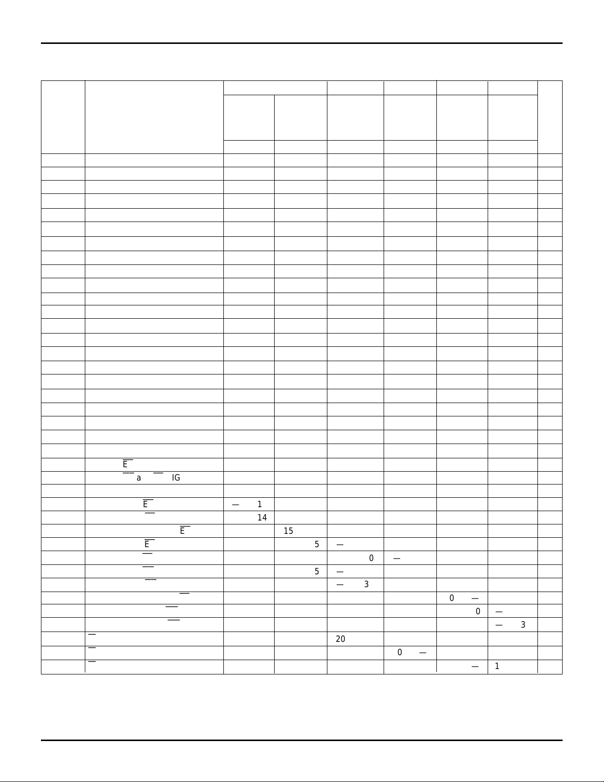
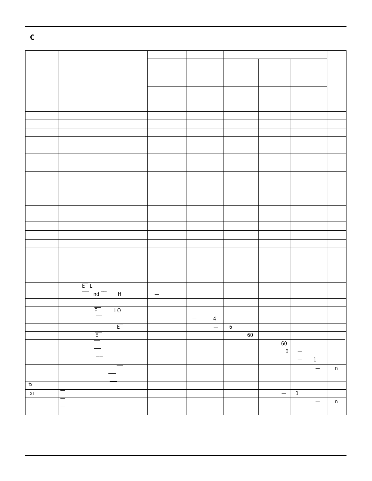
AC ELECTRICAL CHARACTERISTICS
(1)
(Commercial: VCC = 5V ± 10%, TA = 0°C to +70°C; Military: VCC = 5V ± 10%, TA = –55°C to +125°C)
Commercial Com'l & Mil. Com'l Military Com'l
7203S/L12 7203S/L15 7203S/L20 7203S/L25 7203S/L30 7203S/L35
7204S/L12 7204S/L15 7204S/L20 7204S/L25 7204S/L30 7204S/L35
7205L15 7205L20 7205L25 7205L30 7205L35
7206L15 7206L20 7206L25 7206L30 7206L35
Symbol Parameters Min. Max. Min. Max. Min. Max. Min. Max. Min. Max. Min. Max. Unit
f
S Shift Frequency — 50 — 40 — 33.3 — 28.5 — 25 — 22.2 MHz
RC Read Cycle Time 20 — 25 — 30 — 35 — 40 — 45 — ns
t
A Access Time — 12 — 15 — 20 — 25 — 30 — 35 ns
t
t
RR Read Recovery Time 8 — 10 — 10 — 10 — 10 — 10 — ns
RPW Read Pulse Width
t
t
RLZ Read LOW to Data Bus LOW
WLZ Write HIGH to Data Bus Low-Z
t
t
DV Data Valid from Read HIGH 5 — 5 — 5 — 5 — 5 — 5 — ns
RHZ Read HIGH to Data Bus High-Z
t
t
WC Write Cycle Time 20 — 25 — 30 — 35 — 40 — 45 — ns
WPW Write Pulse Width
t
t
WR Write Recovery Time 8 — 10 — 10 — 10 — 10 — 10 — ns
DS Data Set-up Time 9 — 11 — 12 — 15 — 18 — 18 — ns
t
DH Data Hold Time 0 — 0 — 0 — 0 — 0 — 0 — ns
t
t
RSC Reset Cycle Time 20 — 25 — 30 — 35 — 40 — 45 — ns
RS Reset Pulse Width
t
t
RSS Reset Set-up Time
t
RTR Reset Recovery Time 8 — 10 — 10 — 10 — 10 — 10 — ns
RTC Retransmit Cycle Time 20 — 25 — 30 — 35 — 40 — 45 — ns
t
RT Retransmit Pulse Width
t
RTS Retransmit Set-up Time
t
t
RSR Retransmit Recovery Time 8 — 10 — 10 — 10 — 10 — 10 — ns
t
EFL Reset to
HFH, tFFH Reset to
t
RTF Retransmit LOW to Flags Valid — 20 — 25 — 30 — 35 — 40 — 45 ns
t
t
REF Read LOW to
RFF Read HIGH to
t
t
RPE Read Pulse Width after
WEF Write HIGH to
t
t
WFF Write LOW to
WHF Write LOW to
t
RHF Read HIGH to
t
t
WPF Write Pulse Width after
XOL Read/Write LOW to
t
t
XOH Read/Write HIGH to
XI
t
t
XIR
t
XIS
NOTES: 2661 tbl 05
1. Timings referenced as in AC Test Conditions.
2. Pulse widths less than minimum are not allowed.
3. Values guaranteed by design, not currently tested.
4. Only applies to read data flow-through mode.
XI
XI
XI
EF
HF
Pulse Width
Recovery Time 8 — 10 — 10 — 10 — 10 — 10 — ns
Set-up Time 8 — 10 — 10 — 10 — 10 — 15 — ns
(2)
(3)
(2)
(2)
(3)
(2)
(3)
12 — 15 — 20 — 25 — 30 — 35 — ns
3—5—5 — 5—5—5—ns
(3, 4)
3—5—5 — 5—5—10—ns
(3)
— 12 — 15 — 15 — 18 — 20 — 20 ns
12 — 15 — 20 — 25 — 30 — 35 — ns
12 — 15 — 20 — 25 — 30 — 35 — ns
12 — 15 — 20 — 25 — 30 — 35 — ns
12 — 15 — 20 — 25 — 30 — 35 — ns
12 — 15 — 20 — 25 — 30 — 35 — ns
LOW — 12 — 25 — 30 — 35 — 40 — 45 ns
and FF HIGH — 17 — 25 — 30 — 35 — 40 — 45 ns
EF
LOW — 12 — 15 — 20 — 25 — 30 — 30 ns
FF
HIGH — 14 — 15 — 20 — 25 — 30 — 30 ns
EF
HIGH 12 — 15 — 20 — 25 — 30 — 35 — ns
EF
HIGH — 12 — 15 — 20 — 25 — 30 — 30 ns
FF
LOW — 14 — 15 — 20 — 25 — 30 — 30 ns
HF
Flag LOW — 17 — 25 — 30 — 35 — 40 — 45 ns
HF
Flag HIGH — 17 — 25 — 30 — 35 — 40 — 45 ns
FF
HIGH 12 — 15 — 20 — 25 — 30 — 35 — ns
XO
LOW — 12 — 15 — 20 — 25 — 30 — 35 ns
XO
HIGH — 12 — 15 — 20 — 25 — 30 — 35 ns
(2)
12 — 15 — 20 — 25 — 30 — 35 — ns
5.04 4
Page 5
IDT7203/7204/7205/7206 CMOS ASYNCHRONOUS FIFO
2048 x 9, 4096 x 9, 8192 x 9 and 16384 x 9 MILITARY AND COMMERCIAL TEMPERATURE RANGES
AC ELECTRICAL CHARACTERISTICS
(1)
(Continued)
(Commercial: VCC = 5V ± 10%, TA = 0°C to +70°C; Military: VCC = 5V ± 10%, TA = –55°C to +125°C)
Military Com'l & Mil. Military
7203S/L40 7203S/L50 7203S/L65 7203S/L80 7203S/L120
7204S/L40 7204S/L50 7204S/L65 7204S/L80 7204S/L120
7205L50
7206L50
Symbol Parameters Min. Max. Min. Max. Min. Max. Min. Max. Min. Max. Unit
f
S Shift Frequency — 20 — 15 — 12.5 — 10 — 7 MHz
RC Read Cycle Time 50 — 65 — 80 — 100 — 140 — ns
t
t
A Access Time — 40 — 50 — 65 — 80 — 120 ns
RR Read Recovery Time 10 — 15 — 15 — 20 — 20 — ns
t
RPW Read Pulse Width
t
t
RLZ Read LOW to Data Bus LOW
WLZ Write HIGH to Data Bus Low-Z
t
t
DV Data Valid from Read HIGH 5 — 5 — 5 — 5 — 5 — ns
RHZ Read HIGH to Data Bus High-Z
t
t
WC Write Cycle Time 50 — 65 — 80 — 100 — 140 — ns
WPW Write Pulse Width
t
t
WR Write Recovery Time 10 — 15 — 15 — 20 — 20 — ns
DS Data Set-up Time 20 — 30 — 30 — 40 — 40 — ns
t
DH Data Hold Time 0 — 5 — 10 — 10 — 10 — ns
t
t
RSC Reset Cycle Time 50 — 65 — 80 — 100 — 140 — ns
RS Reset Pulse Width
t
t
RSS Reset Set-up Time
t
RSR Reset Recovery Time 10 — 15 — 15 — 20 — 20 — ns
RTC Retransmit Cycle Time 50 — 65 — 80 — 100 — 140 — ns
t
RT Retransmit Pulse Width
t
RTS Retransmit Set-up Time
t
t
RSR Retransmit Recovery Time 10 — 15 — 15 — 20 — 20 — ns
t
EFL Reset to
HFH, tFFH Reset to
t
t
RTF Retransmit LOW to Flags Valid — 50 — 65 — 80 — 100 — 140 ns
REF Read LOW to
t
RFF Read HIGH to
t
t
RPE Read Pulse Width after
WEF Write HIGH to
t
t
WFF Write LOW to
WHF Write LOW to
t
RHF Read HIGH to
t
t
WPF Write Pulse Width after
XOL Read/Write LOW to
t
t
XOH Read/Write HIGH to
XI
t
t
XIR
t
XIS
NOTES: 2661 tbl 06
1. Timings referenced as in AC Test Conditions.
2. Speed grades 65, 80, and 120ns are only available in the ceramic DIP.
3. Pulse widths less than minimum are not allowed.
4. Values guaranteed by design, not currently tested.
5. Only applies to read data flow-through mode.
XI
XI
XI
EF
HF
Pulse Width
Recovery Time 10 — 10 — 10 — 10 — 10 — ns
Set-up Time 15 — 15 — 15 — 15 — 15 — ns
(3)
(4)
(4, 5)
(4)
(3)
(3)
(4)
(3)
(4)
40 — 50 — 65 — 80 — 120 — ns
5 — 10 — 10 — 10 — 10 — ns
10 — 15 — 15 — 20 — 20 — ns
— 25 — 30 — 30 — 30 — 35 ns
40 — 50 — 65 — 80 — 120 — ns
40 — 50 — 65 — 80 — 120 — ns
40 — 50 — 65 — 80 — 120 — ns
40 — 50 — 65 — 80 — 120 — ns
40 — 50 — 65 — 80 — 120 — ns
LOW — 50 — 65 — 80 — 100 — 140 ns
and FF HIGH — 50 — 65 — 80 — 100 — 140 ns
EF
Flag LOW — 35 — 45 — 60 — 60 — 60 ns
FF
HIGH — 35 — 45 — 60 — 60 — 60 ns
EF
HIGH 40 — 50 — 65 — 80 — 120 — ns
EF
HIGH — 35 — 45 — 60 — 60 — 60 ns
FF
LOW — 35 — 45 — 60 — 60 — 60 ns
HF
LOW — 50 — 65 — 80 — 100 — 140 ns
HF
HIGH — 50 — 65 — 80 — 100 — 140 ns
FF
HIGH 40 — 50 — 65 — 80 — 120 — ns
XO
LOW — 40 — 50 — 65 — 80 — 120 ns
XO
HIGH — 40 — 50 — 65 — 80 — 120 ns
(3)
40 — 50 — 65 — 80 — 120 — ns
(2)
5.04 5
Page 6
IDT7203/7204/7205/7206 CMOS ASYNCHRONOUS FIFO
2048 x 9, 4096 x 9, 8192 x 9 and 16384 x 9 MILITARY AND COMMERCIAL TEMPERATURE RANGES
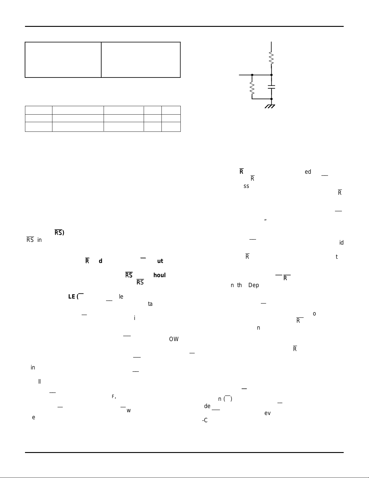
AC TEST CONDITIONS
Input Pulse Levels
Input Rise/Fall Times
Input Timing Reference Levels
Output Reference Levels
Output Load
CAPACITANCE
Symbol Parameter Condition Max. Unit
(1)
C
IN
C
OUT
NOTES: 2661 tbl 08
1. This parameter is sampled and not 100% tested.
2. With output deselected.
Input Capacitance VIN = 0V 10 pF
(1,2)
Output Capacitance VOUT = 0V 10 pF
(1)
(TA = +25°C, f = 1.0 MHz)
GND to 3.0V
5ns
1.5V
1.5V
See Figure 1
2661 tbl 07
SIGNAL DESCRIPTIONS
Inputs:
DATA IN (D0–D8) — Data inputs for 9-bit wide data.
Controls:
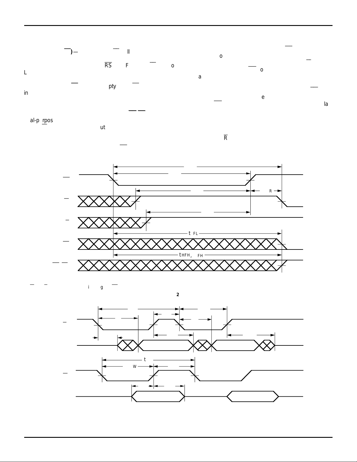
RESET (
(RS) input is taken to a LOW state. During reset, both internal
read and write pointers are set to the first location. A reset is
required after power-up before a write operation can take place.
Both the Read Enable (
be in the HIGH state during the window shown in Figure 2
(i.e. tRSS before the rising edge of
change until tRSR after the rising edge of
WRITE ENABLE (
edge of this input if the Full Flag (FF) is not set. Data set-up and
hold times must be adhered-to, with respect to the rising edge
of the Write Enable (W). Data is stored in the RAM array
sequentially and independently of any on-going read operation.
After half of the memory is filled, and at the falling edge of the
next write operation, the Half-Full Flag (HF) will be set to LOW,
and will remain set until the difference between the write pointer
and read pointer is less-than or equal to one-half of the total
memory of the device. The Half-Full Flag (HF) is reset by the
rising edge of the read operation.
To prevent data overflow, the Full Flag (FF) will go LOW on
the falling edge of the last write signal, which inhibits further write
operations. Upon the completion of a valid read operation, the
Full Flag (FF) will go HIGH after t
to begin. When the FIFO is full, the internal write pointer is
blocked from W, so external changes in W will not affect the FIFO
when it is full.
RSRS) — Reset is accomplished whenever the Reset
RR) and Write Enable (
WW) inputs must
RSRS) and should not
RSRS.
WW) — A write cycle is initiated on the falling
RFF, allowing a new valid write
5V
1.1KΩ
D.U.T.
680Ω
*Includes jig and scope capacitances.
READ ENABLE (
OR EQUIVALENT CIRCUIT
Figure 1. Output Load
RR) — A read cycle is initiated on the falling
30pF*
2661 drw 03
edge of the Read Enable (R), provided the Empty Flag (EF) is not
set. The data is accessed on a First-In/First-Out basis, independent of any ongoing write operations. After Read Enable (R)
goes HIGH, the Data Outputs (Q
0 through Q8) will return to a
high-impedance condition until the next Read operation. When
all the data has been read from the FIFO, the Empty Flag (EF)
will go LOW, allowing the “final” read cycle but inhibiting further
read operations, with the data outputs remaining in a highimpedance state. Once a valid write operation has been accomplished, the Empty Flag (EF) will go HIGH after t
WEF and a valid
Read can then begin. When the FIFO is empty, the internal read
pointer is blocked from R so external changes will not affect the
FIFO when it is empty.
FIRST LOAD/RETRANSMIT (
FLFL/
RTRT) — This is a dual-
purpose input. In the Depth Expansion Mode, this pin is
grounded to indicate that it is the first device loaded (see
Operating Modes). The Single Device Mode is initiated by
grounding the Expansion In (XI).
The IDT7203/7204/7205/7206 can be made to retransmit
data when the Retransmit Enable Control (RT) input is pulsed
LOW. A retransmit operation will set the internal read pointer to
the first location and will not affect the write pointer. The status
of the Flags will change depending on the relative locations of
the read and write pointers. Read Enable (R) and Write Enable
(W) must be in the HIGH state during retransmit. This feature is
useful when less than 2048/4096/8192/16384 writes are performed between resets. The retransmit feature is not compatible with the Depth Expansion Mode.
EXPANSION IN (
XIXI) — This input is a dual-purpose pin.
Expansion In (XI) is grounded to indicate an operation in the
single device mode. Expansion In (XI) is connected to Expansion Out (XO) of the previous device in the Depth Expansion or
Daisy-Chain Mode.
5.04 6
Page 7
IDT7203/7204/7205/7206 CMOS ASYNCHRONOUS FIFO
2048 x 9, 4096 x 9, 8192 x 9 and 16384 x 9 MILITARY AND COMMERCIAL TEMPERATURE RANGES
Outputs:
FULL FLAG (
further write operations, when the device is full. If the read
pointer is not moved after Reset (RS), the Full Flag (FF) will go
LOW after 2048/4096/8192/16384 writes.
EMPTY FLAG (
inhibiting further read operations, when the read pointer is equal
to the write pointer, indicating that the device is empty.
EXPANSION OUT/HALF-FULL FLAG (
dual-purpose output. In the single device mode, when Expansion In (XI) is grounded, this output acts as an indication of a halffull memory.
After half of the memory is filled, and at the falling edge of the
next write operation, the Half-Full Flag (HF) will be set to LOW
FFFF) — The Full Flag (FF) will go LOW, inhibiting
EFEF) — The Empty Flag (EF) will go LOW,
XOXO/
HFHF) — This is a
RS
W
and will remain set until the difference between the write pointer
and read pointer is less than or equal to one half of the total
memory of the device. The Half-Full Flag (HF) is then reset by
the rising edge of the read operation.
In the Depth Expansion Mode, Expansion In (XI) is connected to Expansion Out (XO) of the previous device. This
output acts as a signal to the next device in the Daisy Chain by
providing a pulse to the next device when the previous device
reaches the last location of memory. There will be an XO pulse
when the Write pointer reaches the last location of memory, and
an additional XO pulse when the Read pointer reaches the last
location of memory.
DATA OUTPUTS (Q0-Q8) — Q0-Q8 are data outputs for 9-
bit wide data. These outputs are in a high-impedance condition
whenever Read (R) is in a HIGH state.
t
RSC
t
RS
t
RSS
t
RSR
NOTE:
1. W and R = V
R
EF
HF, FF
IH around the rising edge of
R
Q0–Q
8
W
t
RLZ
RS
t
RSS
t
EFL
t
HFH
, t
FFH
2661 drw 04
.
Figure 2. Reset
t
RC
t
A
t
t
WPW
t
DS
DATA
WC
t
OUT
RR
t
DV
VALID
t
WR
t
DH
t
RPW
t
A
t
RHZ
VALIDDATA
OUT
D
0–D8
DATA
IN
VALID
Figure 3. Asynchronous Write and Read Operation
5.04 7
DATA
IN
VALID
2661 drw 05
Page 8
IDT7203/7204/7205/7206 CMOS ASYNCHRONOUS FIFO
2048 x 9, 4096 x 9, 8192 x 9 and 16384 x 9 MILITARY AND COMMERCIAL TEMPERATURE RANGES
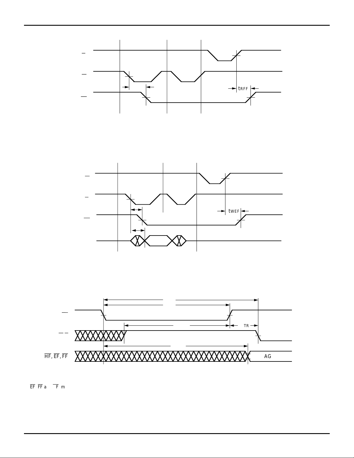
R
W
FF
LAST WRITE
t
WFF
Figure 4. Full FlagTiming From Last Write to First Read
LAST READ
IGNORED
WRITE
IGNORED
READ
FIRST READ
tRFF
2661 drw 06
FIRST WRITE
W
R
t
REF
tWEF
HF, EF, FF
NOTE:
1. EF, FF and HF
EF
t
A
DATA
OUT
Figure 5. Empty Flag Timing From Last Read to First Write
VALID
t
t
RTC
RT
RT
t
RTS
W,R
RTF
may change status during Retransmit, but flags will be valid at tRTC.
t
2661 drw 07
RTR
FLAG VALID
2661 drw 08
Figure 6. Retransmit
5.04 8
Page 9
IDT7203/7204/7205/7206 CMOS ASYNCHRONOUS FIFO
2048 x 9, 4096 x 9, 8192 x 9 and 16384 x 9 MILITARY AND COMMERCIAL TEMPERATURE RANGES
W
t
WEF
EF
t
RPE
R
2661 drw 09
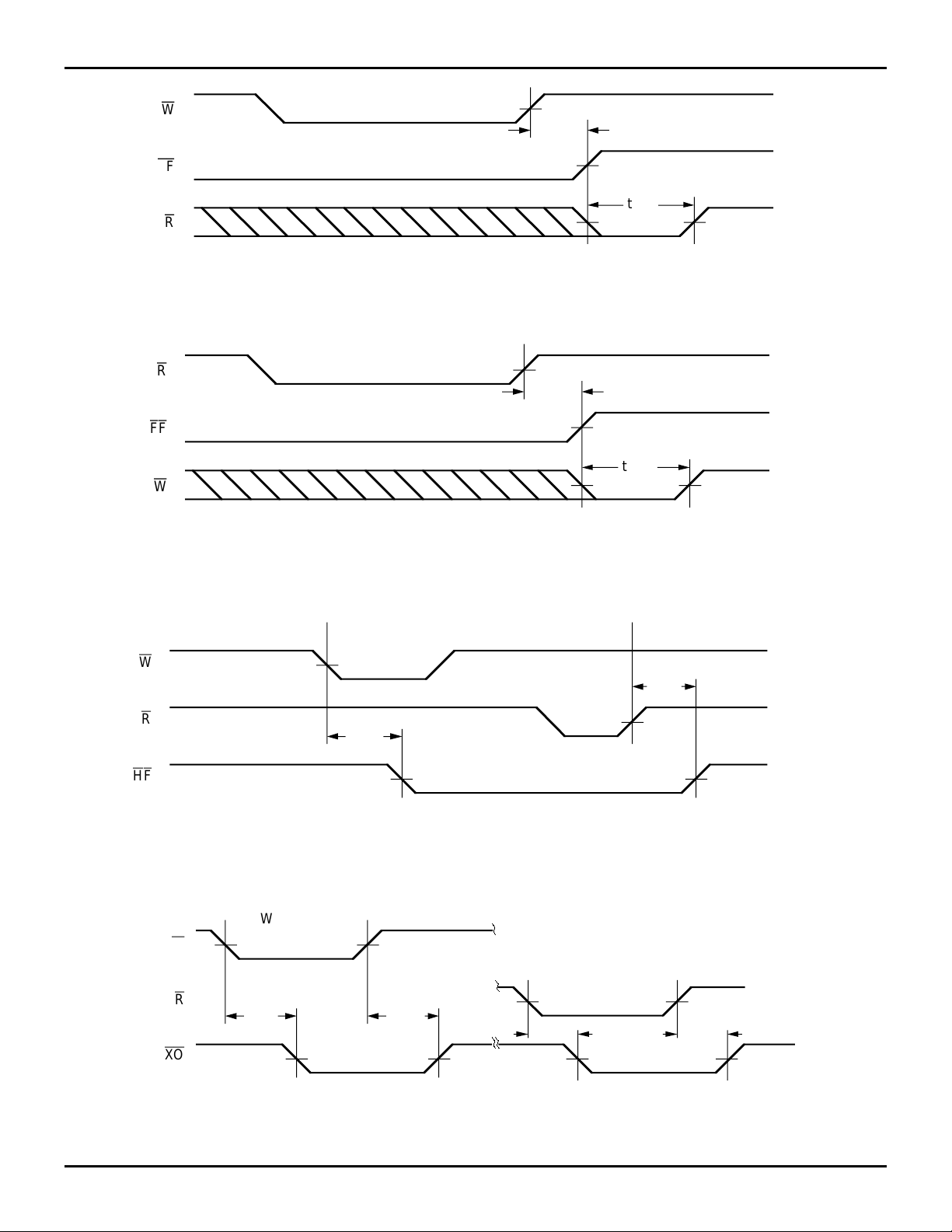
Figure 7. Minimum Timing for an Empty Flag Coincident Read Pulse.
R
t
RFF
FF
t
WPF
W
W
HF
2661 drw 10
Figure 8. Minimum Timing for an Full Flag Coincident Write Pulse.
t
RHF
R
t
WHF
HALF-FULL OR LESS MORE THAN HALF-FULL
Figure 9. Half-Full Flag Timing
HALF-FULL OR LESS
2661 drw 11
WRITE TO
W
LAST PHYSICAL
LOCATION
XO
READ FROM
R
t
XOL
t
XOH
Figure 10. Expansion Out
5.04 9
LAST PHYSICAL
LOCATION
t
XOL
t
XOH
2661 drw 12
Page 10

IDT7203/7204/7205/7206 CMOS ASYNCHRONOUS FIFO
2048 x 9, 4096 x 9, 8192 x 9 and 16384 x 9 MILITARY AND COMMERCIAL TEMPERATURE RANGES
t
XI
XI
t
XIS
W
R
WRITE TO
FIRST PHYSICAL
LOCATION
Figure 11. Expansion In
OPERATING MODES:
Care must be taken to assure that the appropriate flag is
monitored by each system (i.e. FF is monitored on the device
where W is used; EF is monitored on the device where R is
used). For additional information, refer to Tech Note 8:
ating FIFOs on Full and Empty Boundary Conditions
Tech Note 6:
Designing with FIFOs.
Single Device Mode
A single IDT7203/7204/7205/7206 may be used when the
application requirements are for 2048/4096/8192/16384 words
or less. The IDT7203/7204/7205/7206 is in a Single Device
Configuration when the Expansion In (XI) control input is
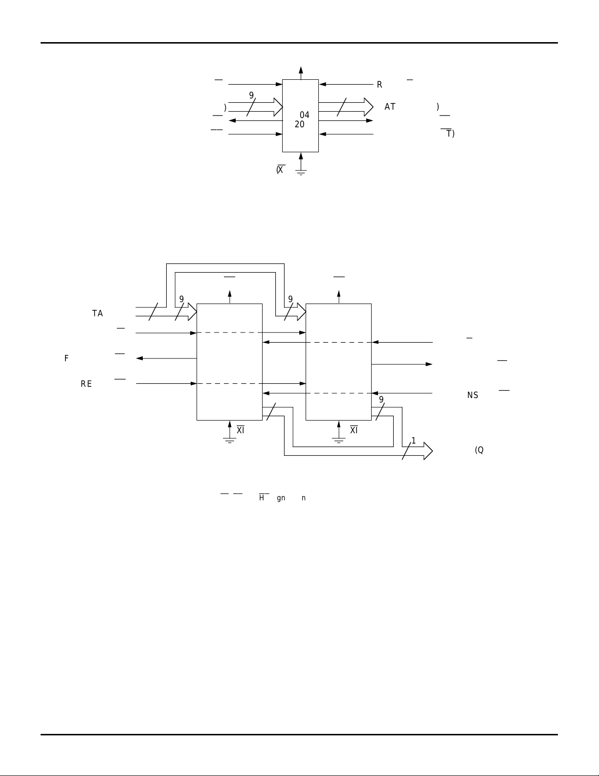
grounded (see Figure 12).
Depth Expansion
The IDT7203/7204/7205/7206 can easily be adapted to
applications when the requirements are for greater than 2048/
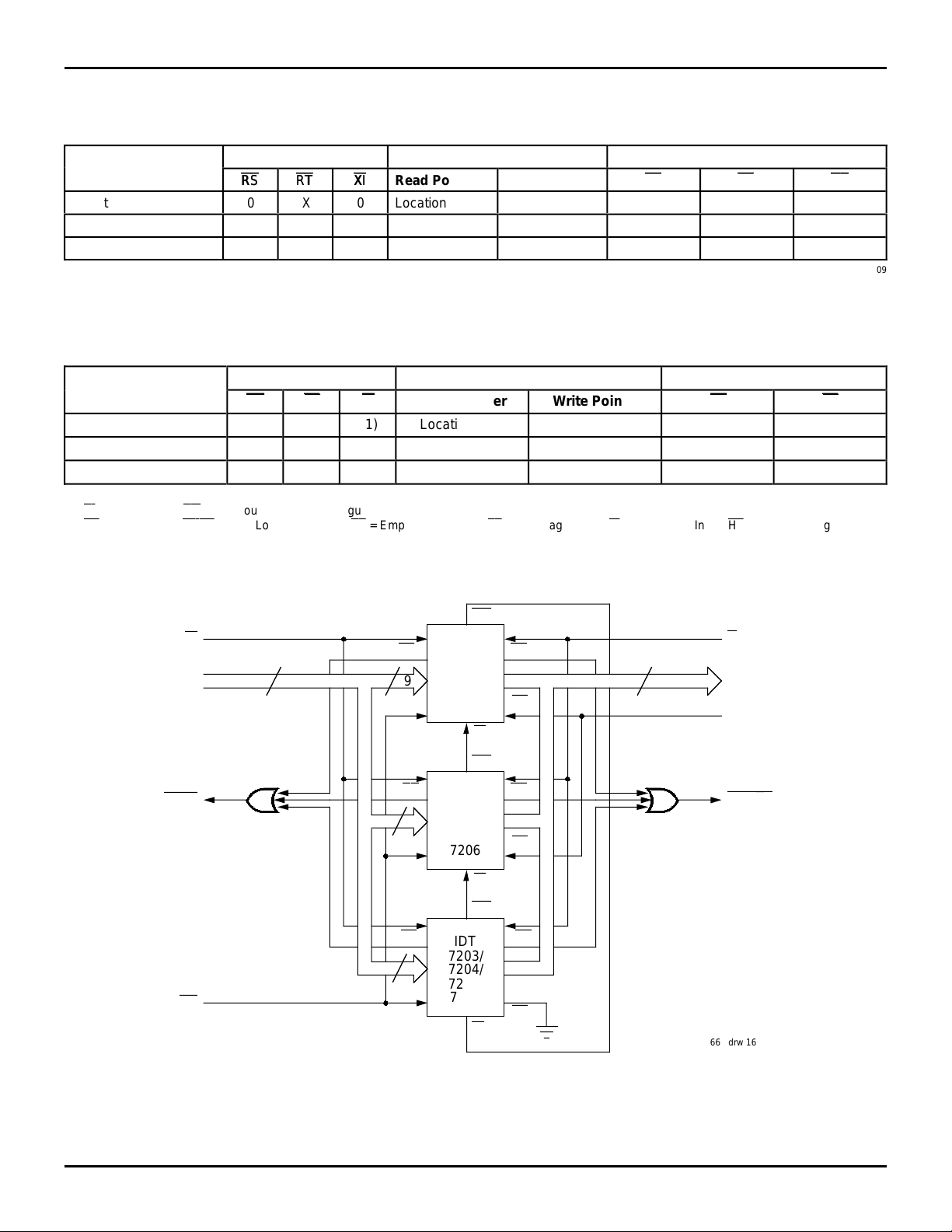
4096/8192/16384 words. Figure 14 demonstrates Depth Expansion using three IDT7203/7204/7205/7206s. Any depth
can be attained by adding additional IDT7203/7204/7205/
7206s. The IDT7203/7204/7205/7206 operates in the Depth
Expansion mode when the following conditions are met:
1. The first device must be designated by grounding the First
Load (FL) control input.
2. All other devices must have FL in the HIGH state.
3. The Expansion Out (XO) pin of each device must be tied to
the Expansion In (XI) pin of the next device. See Figure 14.
4. External logic is needed to generate a composite Full Flag
(FF) and Empty Flag (EF). This requires the ORing of all
EF
s and ORing of all FFs (i.e. all must be set to generate the
correct composite FF or EF). See Figure 14.
5. The Retransmit (RT) function and Half-Full Flag (HF) are
not available in the Depth Expansion Mode.
For additional information, refer to Tech Note 9:
FIFOs or FIFO Modules.
Oper-
and
Cascading
t
XIR
t
XIS
READ FROM
FIRST PHYSICAL
LOCATION
2661 drw 11
USAGE MODES:
Width Expansion
Word width may be increased simply by connecting the
corresponding input control signals of multiple devices. Status flags (EF, FF and HF) can be detected from any one device.
Figure 13 demonstrates an 18-bit word width by using two
IDT7203/7204/7205/7206s. Any word width can be attained
by adding additional IDT7203/7204/7205/7206s (Figure 13).
Bidirectional Operation
Applications which require data buffering between two
systems (each system capable of Read and Write operations)
can be achieved by pairing IDT7203/7204/7205/7206s as
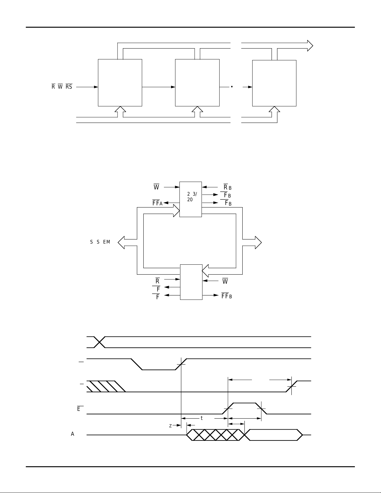
shown in Figure 16. Both Depth Expansion and Width Expansion may be used in this mode.
Data Flow-Through
Two types of flow-through modes are permitted, a read
flow-through and write flow-through mode. For the read flowthrough mode (Figure 17), the FIFO permits a reading of a
single word after writing one word of data into an empty FIFO.
The data is enabled on the bus in (t
edge of W, called the first write edge, and it remains on the bus
until the R line is raised from LOW-to-HIGH, after which the
bus would go into a three-state mode after tRHZ ns. The EF line
would have a pulse showing temporary deassertion and then
would be asserted.
In the write flow-through mode (Figure 18), the FIFO
permits the writing of a single word of data immediately after
reading one word of data from a full FIFO. The R line causes
the FF to be deasserted but the W line being LOW causes it to
be asserted again in anticipation of a new data word. On the
rising edge of W, the new word is loaded in the FIFO. The
line must be toggled when FF is not asserted to write new data
in the FIFO and to increment the write pointer.
Compound Expansion
The two expansion techniques described above can be
applied together in a straightforward manner to achieve large
FIFO arrays (see Figure 15).
WEF + tA) ns after the rising
W
5.04 10
Page 11
IDT7203/7204/7205/7206 CMOS ASYNCHRONOUS FIFO
2048 x 9, 4096 x 9, 8192 x 9 and 16384 x 9 MILITARY AND COMMERCIAL TEMPERATURE RANGES
Figure 12. Block Diagram of 2048 x 9/4096 x 9/8192 x 9/16384 x 9 FIFO Used in Single Device Mode
DATA (D)
IN
WRITE (W)
FULL FLAG (FF)
RESET (RS)
(HALF–FULL FLAG)
WRITE (W)
DATA IN (D)
FULL FLAG (FF)
RESET (RS)
EXPANSION IN (XI)
9918
IDT
7203/
7204/
7205/
7206
(HF)
READ (R)
9
IDT
7203/
7204/
7205/
7206
9
DATA OUT (Q)
EMPTY FLAG (EF)
RETRANSMIT (RT)
2661 drw 14
HFHF
IDT
7203/
7204/
READ (R)
EMPTY FLAG (EF)
7205/
7206
9
9
RETRANSMIT (RT)
XI XI
18
OUT
(Q)
2661 drw 15
DATA
NOTE:
1. Flag detection is accomplished by monitoring the FF, EF and HF signals on either (any) device used in the width expansion configuration.
Do not connect any output signals together.
Figure 13. Block Diagram of 2048 x 18/4096 x 18/8192 x 18/16384 x 18 FIFO Memory Used in Width Expansion Mode
5.04 11
Page 12
IDT7203/7204/7205/7206 CMOS ASYNCHRONOUS FIFO
2048 x 9, 4096 x 9, 8192 x 9 and 16384 x 9 MILITARY AND COMMERCIAL TEMPERATURE RANGES
TRUTH TABLES
TABLE I – RESET AND RETRANSMIT
SINGLE DEVICE CONFIGURATION/WIDTH EXPANSION MODE
Inputs Internal Status Outputs
Mode
RS
RS
RT
RT
XIXIRead Pointer Write Pointer
EF
EF
FF
FF
HF
HF
Reset 0 X 0 Location Zero Location Zero 0 1 1
Retransmit 1 0 0 Location Zero Unchanged X X X
Read/Write 1 1 0 Increment
NOTE:
1. Pointer will Increment if flag is HIGH.
(1)
Increment
(1)
XXX
2661 tbl 09
TABLE II – RESET AND FIRST LOAD
DEPTH EXPANSION/COMPOUND EXPANSION MODE
Inputs Internal Status Outputs
Mode
Reset First Device 0 0 (1) Location Zero Location Zero 0 1
Reset all Other Devices 0 1 (1) Location Zero Location Zero 0 1
Read/Write 1 X (1) X X X X
NOTES:
1. XI is connected to XO of previous device. See Figure 14.
2. RS = Reset Input,
FL/RT
RS
RS
= First Load/Retransmit, EF = Empty Flag Output, FF = Full Flag Output, XI = Expansion Input, HF = Half-Full Flag Output
FL
FL
XI
XI
Read Pointer Write Pointer
EF
EF
FF
FF
2661 tbl 10
W
FULL
RS
XO
FF EF
D
9
99
IDT
7203/
7204/
7205/
7206
FL
R
Q
VCC
XI
XO
FF EF
9
IDT
7203/
7204/
7205/
7206
EMPTY
FL
XI
XO
FF EF
9
IDT
7203/
7204/
7205/
7206
FL
XI
2661 drw 16
Figure 14. Block Diagram of 6149 x 9/12298 x 9/24596 x 9/49152 x 9 FIFO Memory (Depth Expansion)
5.04 12
Page 13
IDT7203/7204/7205/7206 CMOS ASYNCHRONOUS FIFO
2048 x 9, 4096 x 9, 8192 x 9 and 16384 x 9 MILITARY AND COMMERCIAL TEMPERATURE RANGES
Q0–Q8 Q9–Q17
IDT7203/
IDT7204/
IDT7205/
IDT7206
DEPTH
EXPANSION
BLOCK
R, W, RS
IDT7203/
IDT7204/
IDT7205/
IDT7206
DEPTH
EXPANSION
BLOCK
D0 -D8
D9 -DN
NOTES:
1. For depth expansion block see section on Depth Expansion and Figure 14.
2. For Flag detection see section on Width Expansion and Figure 13.
Figure 15. Compound FIFO Expansion
W
FF
A
A
IDT
7203/
IDT
7204/
7201A
7205/
7206
DA 0-8
Q9 –Q17Q0–Q8
D9 -D17
D18 -DN
EF
HF
QB 0-8
Q(N-8) -QN
•••
Q(N-8) -QN
IDT7203/
IDT7204/
IDT7205/
•••
IDT7206
DEPTH
EXPANSION
BLOCK
D(N-8)-DN
•••D0–DN
D(N-8)-DN
R
B
B
B
2661 drw 17
DATA
DATA
SYSTEM A SYSTEM B
A 0-8
IDT
R
A
HF
A
EF
A
Figure 16. Bidirectional FIFO Operation
IN
7203/
7204/
7205/
7206
B 0-8Q
D
W
B
FF
B
W
R
EF
t
WEF
t
A
DATA VALIDOUT
OUT
t
WLZ
2661 drw 18
t
RPE
t
REF
Figure 17. Read Data Flow-Through Mode
5.04 13
2661 drw 19
Page 14
IDT7203/7204/7205/7206 CMOS ASYNCHRONOUS FIFO
2048 x 9, 4096 x 9, 8192 x 9 and 16384 x 9 MILITARY AND COMMERCIAL TEMPERATURE RANGES
R
t
WPF
W
t
RFF
FF
t
DATA
DATA
OUT
WFF
IN
t
A
DATA
Figure 18. Write Data Flow-Through Mode
OUT VALID
DATA IN
t
VALID
DS
t
2661 drw 20
DH
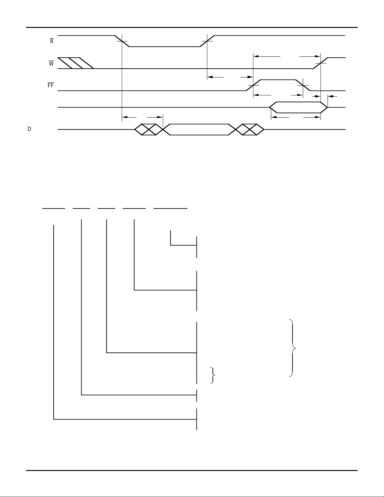
ORDERING INFORMATION
IDT
DeviceType
XXXX
X
PowerXXSpeedXPackage
X
Process/
Temperature
Range
Blank
B
P
TP
D
TD
J
L
SO
12
15
20
25
30
35
40
50
65
80
120
Commercial (0°C to +70°C)
Military (–55°C to +125°C)
Compliant to MIL-STD-883, Class B
Plastic DIP
Plastic THINDIP
Ceramic DIP
Ceramic THINDIP (all except 7206)
Plastic Leaded Chip Carrier
Leadless Chip Carrier (Military only)
Small Outline IC (7204 only)
Commercial 7203/04 Only
Commercial Only
Commercial Only
Military Only
Commercial Only
Access Time (tA)
Speed in ns
Military 7203/04 Only
Military 7203/04DB Only
S
L
7203
7204
7205
7206
5.04 14
Standard Power (7203/7204 only)
Low Power
2048 x 9 FIFO
4096 x 9 FIFO
8192 x 9 FIFO
16384 x 9 FIFO
2661 drw 21
 Loading...