

Datasheet IDT71L024L100PZ, IDT71L024L100PZI, IDT71L024L70PZ, IDT71L024L70PZI Datasheet (Integrated Device Technology Inc)
Integrated Device Technology, Inc.
LOW POWER 3V CMOS SRAM
1 MEG (128K x 8-BIT)
ADVANCE
INFORMATION
IDT71L024
FEATURES:
• 128K x 8 Organization
• Wide Operating Voltage Range: 2.7V to 3.6V
• Speed Grades: 70ns, 100ns
• Low Operating Power: 25mA (max)
• Low Standby Power: 5µA (max)
• Low-Voltage Data Retention: 1.5V (min)
• Available in 32-pin, 13.4mm x 8mm Type I TSOP
package
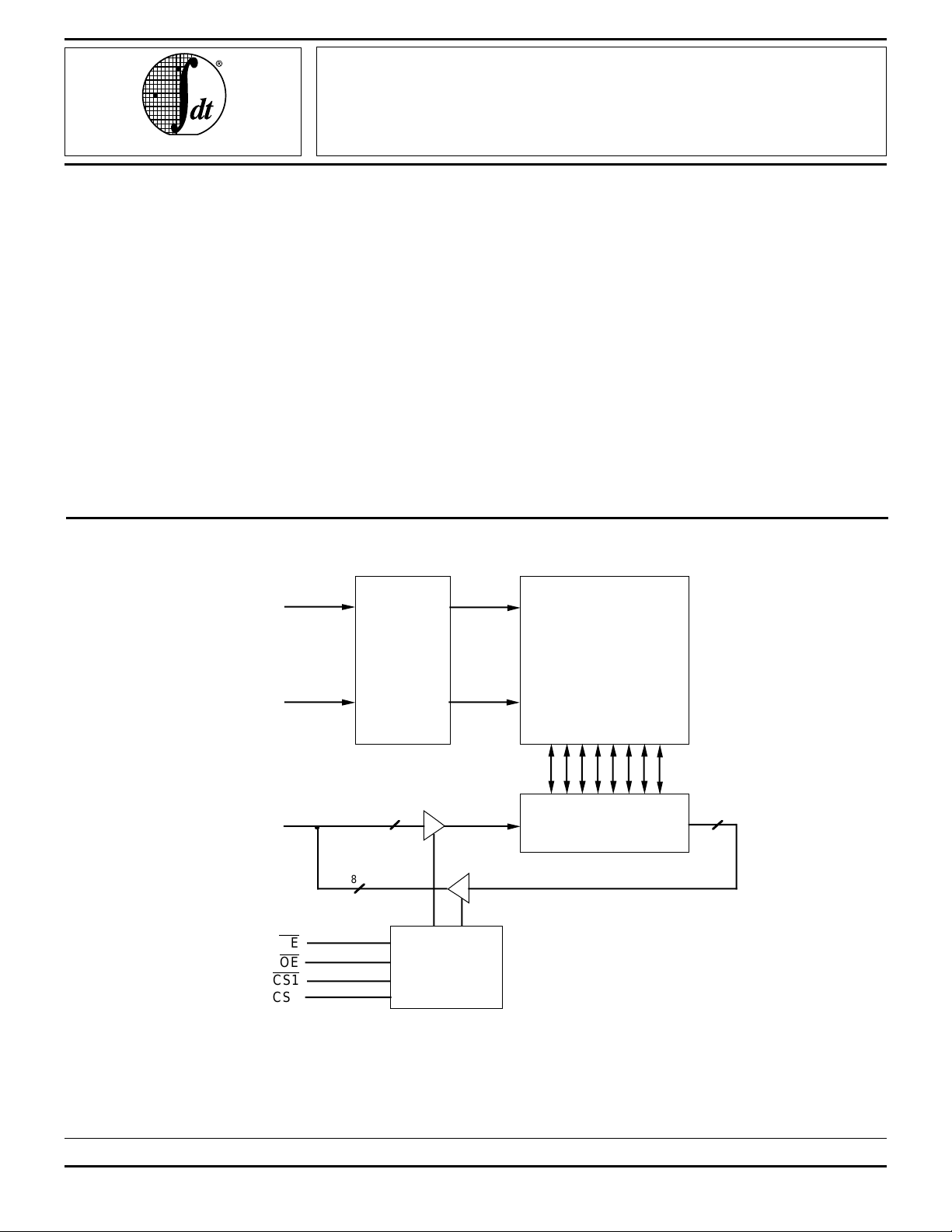
FUNCTIONAL BLOCK DIAGRAM
A0
•
•
•
A16
ADDRESS
DECODER
DESCRIPTION:
The IDT71L024 is a 1,048,576-bit very low-power Static
RAM organized as 128K x 8. It is fabricated using IDT’s highreliability CMOS technology. This state-of-the-art technology,
combined with innovative circuit design techniques, provides
a cost-effective solution for low-power memory needs. It uses
a 6-transistor memory cell.
All input and output signals of the IDT71L024 are LVTTLcompatible and operation is from a single extended-range
3.3V supply. This extended supply range makes the device
ideally suited for unregulated battery-powered applications.
Fully static asynchronous circuitry is used, requiring no clocks
or refresh for operation.
The IDT71L024 is packaged in a JEDEC standard 32-pin
TSOP Type I.
•
•
1,048,576-BIT
MEMORY ARRAY
•
I/O0 – I/O7
The IDT logo is a registered trademark of Integrated Device Technology, Inc.
•
8
WE
OE
CS1
CS2
8
CONTROL
LOGIC
I/O CONTROL
8
3778 drw 01
INDUSTRIAL AND COMMERCIAL TEMPERATURE RANGES MAY 1997
1997 Integrated Device Technology, Inc. DSC-3967/-
1
IDT71L024
LOW POWER 3V CMOS STATIC RAM 1 MEG (128K x 8-BIT) COMMERCIAL AND INDUSTRIAL TEMPERATURE RANGES
PIN CONFIGURATIONS
11
A
A9
A8
A13
WE
CS2
A
VDD
NC
A16
A14
A12
A7
A6
A5
1
2
3
4
5
6
15
7
8
9
10
11
12
13 20
14 19
15 18
16A4 17
TSOP (I)
TSOP
TOP VIEW
32
31
30
29
28
27
26
25
24
23
22
21
3778 drw 02
OE
A10
CS1
I/O
I/O6
I/O5
I/O4
I/O3
VSS
I/O2
I/O1
I/O0
A0
A1
A2
A3
7
TRUTH TABLE
CS1
CS2
CS1
(1)
OEOEWEWE I/O0-I/O7 Function
H X X X High-Z Deselected - Standby
X L X X High-Z Deselected - Standby
L H L H DATA
L H X L DATA
OUT Read
IN Write
L H H H High-Z Outputs Disabled
NOTE: 3778 tbl 02
1.H = VIH, L = VIL, X = Don't care.
PIN DESCRIPTIONS
A0 – A16 Address Inputs Input
CS1
Chip Select Input
CS2 Chip Select Input
WE
OE
I/O
0 - I/O7 Data Input/Output I/O
V
DD Power Pwr
V
SS Ground Gnd
Write Enable Input
Output Enable Input
3778 tbl 01
CAPACITANCE
(TA = +25°C, f = 1.0MHz)
Symbol Parameter
IN Input Capacitance VIN = 3dV 6 pF
C
I/O I/O Capacitance VOUT = 3dV 7 pF
C
NOTE: 3778 tbl 06
1. This parameter is guaranteed by device characterization, but not production tested.
(1)
Conditions Max. Unit
2
IDT71L024
LOW POWER 3V CMOS STATIC RAM 1 MEG (128K x 8-BIT) COMMERCIAL AND INDUSTRIAL TEMPERATURE RANGES
ABSOLUTE MAXIMUM RATINGS
(1)
Symbol Rating Com’l. and Ind'l. Unit
(2)
TERM
V
VTERM
Terminal Voltage with –0.5 to +4.6 V
Respect to V
(3)
Terminal Voltage with –0.5 to VDD+0.5V V
Respect to V
SS
SS
TBIAS Temperature Under Bias –55 to +125 °C
STG Storage Temperature –55 to +125 °C
T
T Power Dissipation 1.0 W
P
OUT DC Output Current 20 mA
I
NOTES: 3778 tbl 03
1. Stresses greater than those listed under ABSOLUTE MAXIMUM
RATINGS may cause permanent damage to the device. This is a stress
rating only and functional operation of the device at these or any other
conditions above those indicated in the operational sections of this
specification is not implied. Exposure to absolute maximum rating
conditions for extended periods may affect reliability.
2. V
DD terminals only.
3. Input, Output,and I/O terminals; 4.6V maximum.
RECOMMENDED OPERATING
TEMPERATURE AND SUPPLY VOLTAGE
Grade Temperature VSS VDD
Commercial 0°C to +70°C 0V 2.7V to 3.6V
Industrial -40°C to +85°C 0V 2.7V to 3.6V
3778 tbl 04
RECOMMENDED DC OPERATING
CONDITIONS
Symbol Parameter Min. Typ. Max. Unit
VDD Supply Voltage 2.7 3.0 3.6 V
VSS Ground 0 0 0 V
VIH Input High Voltage 2.0 — VDD+0.3
V
IL Input Low Voltage –0.3
NOTE: 3778 tbl 05
1. VIH (max.) = VDD + 1.5V for pulse width less than 5ns, once per cycle.
2. V
IL (min.) = –1.5V for pulse width less than 5ns, once per cycle.
(2)
— 0.8 V
(1)
V
DC ELECTRICAL CHARACTERISTICS
VDD = 2.7V to 3.6V, Commercial and Industrial Temperature Ranges
Symbol Parameter Test Conditions Min. Max. Unit
LI| Input Leakage Current VDD = Max., VIN = VSS to VDD — 1 µA
|I
LO| Output Leakage Current VDD = Max.,
|I
OH Output High Voltage IOH = –1mA, VDD = Min. 2.4 — V
V
OL Output Low Voltage IOL = 2mA, VDD = Min. — 0.4 V
V
DC ELECTRICAL CHARACTERISTICS
VDD = 2.7 to 3.6V, VLC = 0.2V, VHC = VDD–0.2V, Commercial and Industrial Temperature Ranges
Symbol Parameter Test Conditions Typ.
CC2 Dynamic Operating Current
I
CC Static Operating Current
I
ISB1 Standby Supply Current
NOTES: 3778 tbl 08
1. All values are maximum guaranteed values.
2. Input low and high voltage levels are 0.2V and V
MAX = 1/tRC (all address inputs are cycling at fMAX).
3. f
4. f = 0 means no address input lines are changing
5. Typical conditions are VDD = 3.0V and specified temperature.
CS1
= VLC, CS2 = VHC, Outputs Open, -70 ns — 25 mA
V
DD = 3.6V, f = fMAX
CS1
= VLC, CS2 = VHC, Outputs Open, — 5 mA
WE
= V
HC, VDD = 3.6V, f = 0
CS1
and CS2 = VHC, or CS2 = VLC, -40 to 85°C— 10 µA
Outputs Open, V
DD-0.2V respectively for all tests.
.
CS
= VIH, VOUT = VSS to VDD — 1 µA
(1, 2)
(5)
(3)
(4)
DD = 3.6V 0 to 70°C— 5
-100 ns — 18
40°C—2
25°C—1
3778 tbl 07
Max. Unit
3

IDT71L024
LOW POWER 3V CMOS STATIC RAM 1 MEG (128K x 8-BIT) COMMERCIAL AND INDUSTRIAL TEMPERATURE RANGES
DATA RETENTION CHARACTERISTICS OVER ALL TEMPERATURE RANGES
(VLC = 0.2V, VHC = VDD - 0.2V)
Symbol Parameter Test Condition Min. Typ.
DR VCC for Data Retention — 1.5 — — V
V
CCDR Data Retention Current 1)
I
(3)
CDR
t
Chip Deselect to Data or 0 — — ns
CS1
≥ VHC and CS2 ≥ VHC —<1 5µA
Retention Time 2) CS2 ≤ VLC
(3)
t
R
NOTES: 3778 tbl 09
1. TA = +25°C.
RC = Read Cycle Time.
2. t
3. This parameter is guaranteed by device characterization, but is not production tested.
Operation Recovery Time tRC
(2)
(1)
Max. Unit
——ns
LOW VDD DATA RETENTION WAVEFORM
DATA
RETENTION
MODE
VDD
2.7V 2.7V
V
CS
IH VIH
AC TEST CONDITIONS
Input Pulse Levels GND to 2.5V
Input Rise/Fall Times 3ns
Input Timing Reference Levels 1.5V
Output Reference Levels 1.5V
AC Test Load See Figure 1
3778 tbl 10
V
DR ≥ 1.5V
DR
V
AC TEST LOAD
DATA
OUT
50pF*
tRtCDR
3778 drw 05
VDD
3070Ω
3150Ω
3778 drw 04
*Including jig and scope capacitance.
Figure 1. AC Test Load
4

IDT71L024
LOW POWER 3V CMOS STATIC RAM 1 MEG (128K x 8-BIT) COMMERCIAL AND INDUSTRIAL TEMPERATURE RANGES
AC ELECTRICAL CHARACTERISTICS (VDD = 2.7 to 3.6V, All Temperature Ranges)
71L024L70 71L024L100
Symbol Parameter Min. Max. Min. Max. Units
Read Cycle
RC Read Cycle Time 70 — 100 — ns
t
AA Address Access Time — 70 — 100 ns
t
ACS Chip Select Access Time — 70 — 100 ns
t
(1)
CLZ
t
(1)
CHZ
t
OE Output Enable Low to Output Valid — 35 — 50 ns
t
(1)
OLZ
t
(1)
OHZ
t
OH Output Hold from Address Change 10 — 15 — ns
t
Write Cycle
WC Write Cycle Time 70 — 100 — ns
t
AW Address Valid to End of Write 65 — 80 — ns
t
CW Chip Select Low to End of Write 65 — 80 — ns
t
AS Address Set-up Time 0 — 0 — ns
t
WR Address Hold from End of Write 0 — 0 — ns
t
WP Write Pulse Width 55 — 70 — ns
t
DW Data Valid to End of Write 30 — 40 — ns
t
DH Data Hold Time 0 — 0 — ns
t
(1)
OW
t
(1)
WHZ
t
NOTE: 3778 tbl 11
1. This parameter is guaranteed by device characterization, but is not production tested.
Chip Select Low to Output in Low-Z 10 — 10 — ns
Chip Select High to Output in High-Z — 25 — 30 ns
Output Enable Low to Output in Low-Z 5 — 5 — ns
Output Enable High to Output in High-Z — 25 — 30 ns
Write Enable High to Output in Low-Z 5 — 5 — ns
Write Enable Low to Output in High-Z — 25 — 30 ns
5

IDT71L024
LOW POWER 3V CMOS STATIC RAM 1 MEG (128K x 8-BIT) COMMERCIAL AND INDUSTRIAL TEMPERATURE RANGES
TIMING WAVEFORM OF READ CYCLE NO. 1
ADDRESS
t
AA
OE
(5)
t
t
CLZ
OLZ
t
ACS
(5)
DATA
CS1
CS2
OUT
HIGH IMPEDANCE
(1)
t
RC
OE
t
(3)
(5)
t
OHZ
(5)
t
CHZ
DATA VALID
OUT
3778 drw 06
TIMING WAVEFORM OF READ CYCLE NO. 2
ADDRESS
tAA
tOH tOH
DATAOUT
NOTES:
1.WE is HIGH for Read Cycle.
2. Device is continuously selected;
3. Address must be valid prior to or coincident with the later of
4.OE is LOW.
5. Transition is measured ±200mV from steady state.
CS1
is LOW and CS2 is HIGH.
CS1
transition LOW and CS2 transition HIGH; otherwise t
(1, 2, 4)
tRC
DATAOUT VALIDPREVIOUS DATAOUT VALID
3778 drw 07
AA is the limiting parameter.
6

IDT71L024
LOW POWER 3V CMOS STATIC RAM 1 MEG (128K x 8-BIT) COMMERCIAL AND INDUSTRIAL TEMPERATURE RANGES
TIMING WAVEFORM OF WRITE CYCLE NO. 1 (
t
ADDRESS
tAW
tCW
tWHZ
tWP
(6)
DATA
DATAIN
CS1
CS2
tAS
WE
OUT
WEWE CONTROLLED TIMING)
WC
(3)
(7)
HIGH IMPEDANCE
tDW
DATAIN VALID
tWR
tOW
tDH
(6)
(1, 2, 5)
(6)
tCHZ
(4)(4)
3778 drw 09
TIMING WAVEFORM OF WRITE CYCLE NO. 2 (
CS1
AND CS2 CONTROLLED TIMING)
CS1
tWC
ADDRESS
tAW
CS1
CS2
tAS
tCW
WE
tDW
DATA
IN
NOTES:
1.WE or
2. A write occurs during the overlap of a LOW
3. t
4. During this period, I/O pins are in the output state, and input signals must not be applied.
5. If the
6. Transition is measured ±200mV from steady state.
7.OE is continuously HIGH. If during a WE controlled write cycle OE is LOW, t
CS1
must be HIGH, or CS2 must be LOW during all address transitions.
WR is measured from the earlier of either
CS1
LOW transition or CS2 HIGH transition occurs simultaneously with or after the WE LOW transition, the outputs remain in a high-impedance state.
off and data to be placed on the bus for the required t
minimum write pulse is as short as the specified t
CS1
, HIGH CS2, and a LOW WE.
CS1
or WE going HIGH or CS2 going LOW to the end of the write cycle.
WP.
DW. If
OE
is HIGH during a WE controlled write cycle, this requirement does not apply and the
WP must be greater than or equal to tWHZ + tDW to allow the I/O drivers to turn
tWR
DATAIN VALID
(1,2,5)
(3)
tDH
3778 drw 10
7

IDT71L024
LOW POWER 3V CMOS STATIC RAM 1 MEG (128K x 8-BIT) COMMERCIAL AND INDUSTRIAL TEMPERATURE RANGES
ORDERING INFORMATION
IDT
71L024
Device
Type
L
Power
XXX
SpeedXXPackage
X
Process/
Temperature
Range
Blank
I
PZ
70
100
Commercial (0°C to +70°C)
Industrial (-40°C to +85°C)
8mm x 13.4mm TSOP Type I
Speed in nanoseconds
3778 drw 11
8
 Loading...