

Datasheet IDT7187L25DB, IDT7187L35DB, IDT7187L35L22B, IDT7187L45DB, IDT7187L55DB Datasheet (Integrated Device Technology Inc)
...Page 1
Integrated Device Technology, Inc.
CMOS STATIC RAM
64K (64K x 1-BIT)
IDT7187S
IDT7187L
FEATURES:
• High speed (equal access and cycle time)
— Military: 25/35/45/55/70/85ns (max.)
• Low power consumption
• Battery backup operation—2V data retention (L version
only)
• JEDEC standard high-density 22-pin ceramic DIP, 22-pin
leadless chip carrier
• Produced with advanced CMOS high-performance
technology
• Separate data input and output
• Input and output directly TTL-compatible
• Military product compliant to MIL-STD-883, Class B
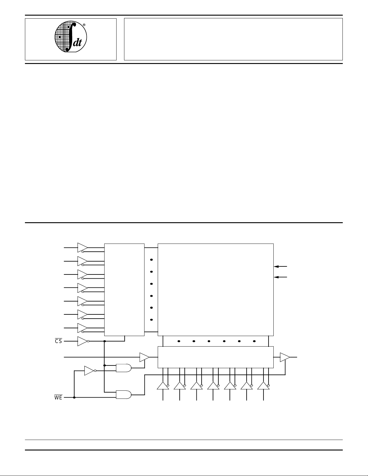
FUNCTIONAL BLOCK DIAGRAM
A
DESCRIPTION:
The IDT7187 is a 65,536-bit high-speed static RAM
organized as 64K x 1. It is fabricated using IDT’s highperformance, high-reliability CMOS technology. Access times
as fast as 25ns are available.
Both the standard (S) and low-power (L) versions of the
IDT7187 provide two standby modes—ISB and ISB1. ISB
provides low-power operation; ISB1 provides ultra-low-power
operation. The low-power (L) version also provides the capability for data retention using battery backup. When using a 2V
battery, the circuit typically consumes only 30µW.
Ease of system design is achieved by the IDT7187 with full
asynchronous operation, along with matching access and
cycle times. The device is packaged in an industry standard
22-pin, 300 mil ceramic DIP, or 22-pin leadless chip carriers.
Military grade product is manufactured in compliance with
the latest revision of MIL-STD-883, Class B, making it ideally
suited to military temperature applications demanding the
highest level of performance and reliability.
DATA
A
A
A
A
A
A
CS
IN
WE
ROW
SELECT
65,536-BIT
MEMORY ARRAY
COLUMN I/O
AAAAAAA
V
CC
GND
DATA
2986 drw 01
OUT
The IDT logo is a registered trademark of Integrated Device Technology, Inc.
MILITARY TEMPERATURE RANGE AUGUST 1996
1996 Integrated Device Technology, Inc. 2986/7
For latest information contact IDT's web site at www.idt.com or fax-on-demand at 408-492-8391.
6.2
1
Page 2
IDT7187S/L
CMOS STATIC RAM 64K (64K x 1-BIT) MILITARY TEMPERATURE RANGE
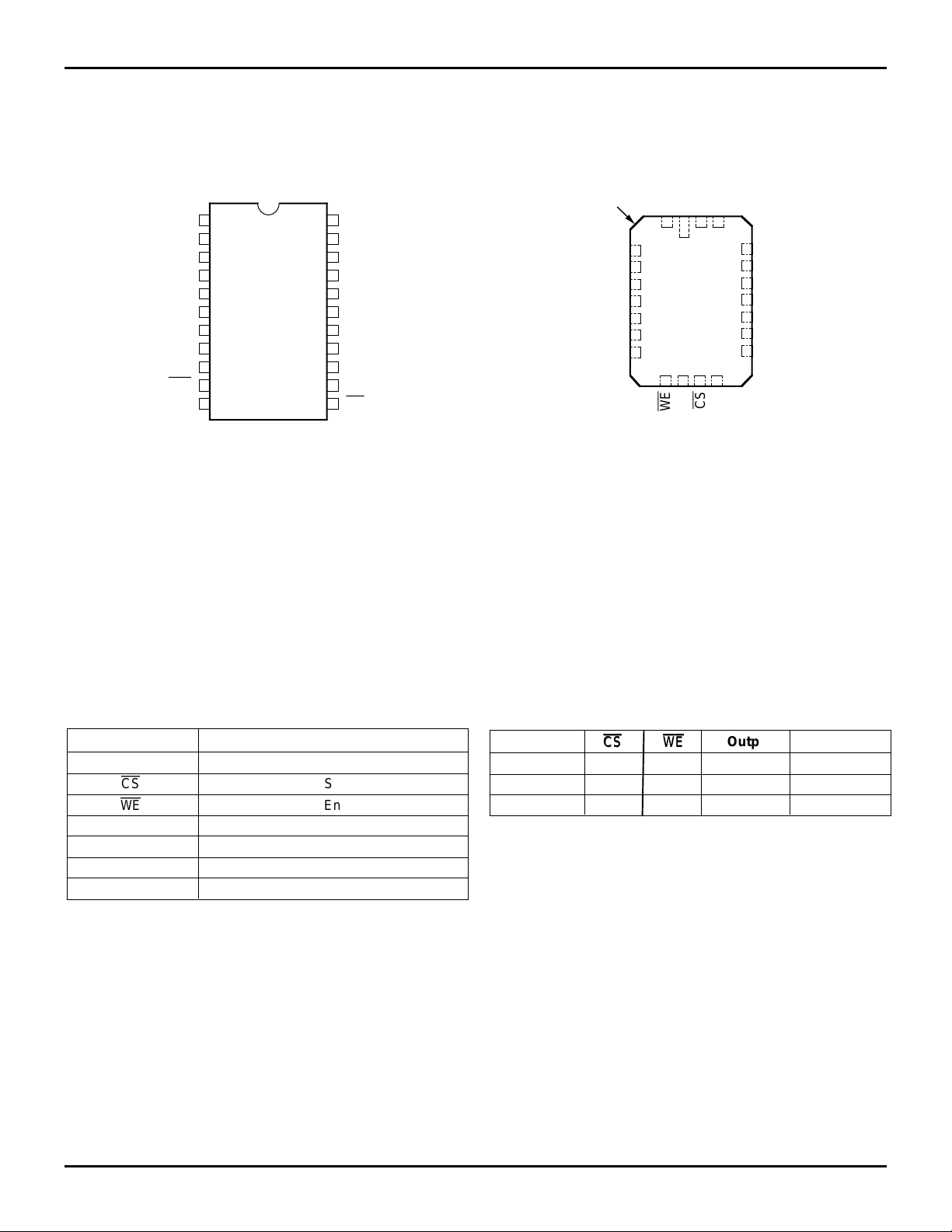
PIN CONFIGURATIONS
0
1
A0
2
A1
3
A2
4
A3
5
A4
6
A
5
A6
A7
DATA
OUT
WE
GND CS
D22-1
7
8
9
10
11
22
21
20
19
18
17
16
15
14
13
12
VCC
A15
A14
A13
A12
A11
A10
A9
A8
DATAIN
2986 drw 02
INDEX
A2
A3
A4
A5
A6
A7
DATAOUT
1
A
2
3
4
5
L22-1
6
7
8
9
10 11 12 13
WE
A
1
GND
VCC
22 21
CS
15
A
20
19
18
17
16
15
14
IN
2986 drw 03
DATA
A14
A13
A12
A11
A10
A
A8
9
DIP
TOP VIEW
PIN DESCRIPTIONS
Name Description
A
0–A15 Address Inputs
CS
WE
V
CC Power
DATA
IN Data Input
DATA
OUT Data Output
GND Ground
Chip Select
Write Enable
2986 tbl 01
22-PIN LCC
TOP VIEW
CS
CS
(1)
WE
WE
Output Power
TRUTH TABLE
Mode
Standby H X High-Z Standby
Read L H D
OUT Active
Write L L High-Z Active
NOTE: 2986 tbl 02
1. H = VIH, L = VIL, X = don't care.
6.2 2
Page 3
IDT7187S/L
CMOS STATIC RAM 64K (64K x 1-BIT) MILITARY TEMPERATURE RANGE
ABSOLUTE MAXIMUM RATINGS
(1)
Symbol Rating Com’l. Mil. Unit
V
TERM Terminal Voltage –0.5 to +7.0 –0.5 to +7.0 V
with Respect
to GND
T
A Operating 0 to +70 –55 to +125 °C
Temperature
T
BIAS Temperature –55 to +125 –65 to +135 °C
Under Bias
T
STG Storage –55 to +125 –65 to +150 °C
Temperature
P
T Power Dissipation 1.0 1.0 W
I
OUT DC Output 50 50 mA
Current
NOTE: 2986 tbl 03
1. Stresses greater than those listed under ABSOLUTE MAXIMUM
RATINGS may cause permanent damage to the device. This is a stress
rating only and functional operation of the device at these or any other
conditions above those indicated in the operational sections of this
specification is not implied. Exposure to absolute maximum rating
conditions for extended periods may affect reliability.
CAPACITANCE (TA = +25°C, F = 1.0MHZ)
Symbol Parameter
C
IN Input Capacitance VIN = 0V 8 pF
C
OUT Output Capacitance VOUT = 0V 8 pF
NOTE: 2986 tbl 04
1. This parameter is determined by device characterization, but is not
production tested.
(1)
Conditions Max. Unit
RECOMMENDED DC OPERATING
CONDITIONS
Symbol Parameter Min. Typ. Max. Unit
V
CC Supply Voltage 4.5 5.0 5.5 V
G
ND Supply Voltage 0 0 0 V
V
IH Input High Voltage 2.2 — 6.0 V
V
IL Input Low Voltage –0.5
NOTE: 2986 tbl 05
1. VIL (min.) = –3.0V for pulse width less than 20ns, once per cycle.
(1)
— 0.8 V
RECOMMENDED OPERATING
TEMPERATURE AND SUPPLY VOLTAGE
Grade Temperature GND VCC
Military –55°C to +125°C 0V 5V ± 10%
Commercial 0°C to +70°C 0V 5V ± 10%
2986 tbl 06
DC ELECTRICAL CHARACTERISTICS
(VCC = 5.0V ± 10%)
IDT7187S IDT7187L
Symbol Parameter Test Condition Min. Max. Min. Max. Unit
|I
LI| Input Leakage Current VCC = Max., MIL. — 10 — 5 µA
V
IN = GND to VCC COM’L. — 5 — 2
|I
LO| Output Leakage Current VCC = Max.,
V
OUT = GND to VCC COM’L. — 5 — 2
V
OL Output Low Voltage IOL = 10mA, VCC = Min. 0.5 — 0.5 V
I
OL = 8mA, VCC = Min. — 0.4 — 0.4
V
OH Output High Voltage IOH = –4mA, VCC = Min. 2.4 — 2.4 — V
CS
= VIH, MIL. — 10 — 5 µ A
2986 tbl 07
6.2 3
Page 4

IDT7187S/L
CMOS STATIC RAM 64K (64K x 1-BIT) MILITARY TEMPERATURE RANGE
DC ELECTRICAL CHARACTERISTICS
(1)
(VCC = 5V ± 10%, VLC = 0.2V, VHC = VCC - 0.2V)
7187S25 7187S35 7187S45 7187S55/70 7187S85
7187L25 7187L35 7187L45 7187L55/70 7187L85
Symbol Parameter Power Com’l. Mil. Com’l. Mil. Com’l. Mil. Com’l. Mil. Com’l. Mil. Unit
CC1 Operating Power S — 105 — 105 — 105 — 105 — 105 mA
I
Supply Current
CS
= V
IL, Outputs Open L — 85 — 85 — 85 — 85 — 85
VCC = Max., f = 0
ICC2 Dynamic Operating S — 130 — 120 — 120 — 120 — 120 mA
Current
CS
= V
IL, Outputs Open L — 110 — 100 — 95 — 90 — 90
VCC = Max., f = fMAX
ISB Standby Power Supply S — 55 — 50 — 50 — 50 — 50 mA
Current (TTL Level)
CS
≥ V
IH, VCC = Max., L — 50 — 40 — 35 — 30/28 — 28
Outputs Open, f = fMAX
ISB1 Full Standby Power S — 20 — 20 — 20 — 20 — 20 mA
Supply Current (CMOS
Level) CS ≥ V
V
CC=Max., VIN ≥ VHC or
V
IN ≤ VLC, f = 0
NOTES: 2986 tbl 08
1. All values are maximum guaranteed values.
2. At f = f
MAX address and data inputs are cycling at the maximum frequency of read cycles of 1/tRC. f = 0 means no input lines change.
(2)
(2)
(2)
HC, L — 1.5 — 1.5 — 1.5 — 1.5 — 1.5
(2)
DATA RETENTION CHARACTERISTICS OVER ALL TEMPERATURE RANGES
(L Version Only) VHC = VCC - 0.2V, VLC = 0.2V
(1)
Typ.
V
CC @VCC @
Symbol Parameter Test Condition Min. 2.0v 3.0V 2.0V 3.0V Unit
DR VCC for Data Retention — 2.0 — — — — V
V
CCDR Data Retention Current MIL. — 10 15 600 900 µA
I
COM’L. — 10 15 150 225
(3)
t
CDR
(3)
tR
(3)
LI|
|I
NOTES: 2986 tbl 09
1. TA = +25°C.
RC = Read Cycle Time.
2. t
3. This parameter is guaranteed, but not tested.
Chip Deselect to Data
Retention Time V
Operation Recovery Time tRC
CS
≥ VHC 0————ns
IN ≥ VHC or ≤ VLC
(2)
————ns
Input Leakage Current — — — 2 2 µA
Max.
LOW VCC DATA RETENTION WAVEFORM
DATA
RETENTION
MODE
VCC
tCDR
4.5V
DR ≥2V
V
4.5V
tR
CS
V
IH
DR
V
6.2 4
VIH
2986 drw 04
Page 5

IDT7187S/L
CMOS STATIC RAM 64K (64K x 1-BIT) MILITARY TEMPERATURE RANGE
AC TEST CONDITIONS
Input Pulse Levels GND to 3.0V
Input Rise/Fall Times 5ns
Input Timing Reference Levels 1.5V
Output Reference Levels 1.5V
AC Test Load See Figures 1 and 2
2986 tbl 10
5V
480Ω
5pF*
2986 drw 06
DATA
5V
480
Ω
OUT
255
Ω
Figure 1. AC Test Load Figure 2. AC Test Load
30pF*
2986 drw 05
*Includes scope and jig capacitances
DATA
OUT
255Ω
(for t
HZ, tLZ, tWZ and tOW)
AC ELECTRICAL CHARACTERISTICS (VCC = 5.0V ± 10%, All Temperature Ranges)
7187S25 7187S35/45
7187L25 7187L35/45
(1)
(1)
7187S55
7187L55
Symbol Parameter Min. Max. Min. Max. Min. Max. Min. Max. Min. Max. Unit
Read Cycle
tRC Read Cycle Time 25 — 35/45 — 55 — 70 — 85 — ns
tAA Address Access Time — 25 — 35/45 — 55 — 70 — 85 ns
tACS Chip Select Access Time — 25 — 35/45 — 55 — 70 — 85 ns
tOH Output Hold from Address Change 5 — 5 — 5 — 5 — 5 — ns
(2)
tLZ
tHZ
tPU
PD
t
NOTES: 2986 tbl 11
1. –55°C to +125°C temperature range only.
2. This parameter guaranteed but not tested.
Output Selection to Output in Low-Z 5 — 5 — 5 — 5 — 5 — ns
(2)
Chip Deselect to Output in High-Z — 12 — 17/20 — 30 — 30 — 40 ns
(2)
Chip Select to Power-Up Time 0 — 0 — 0 — 0 — 0 — ns
(2)
Chip Deselect to Power-Down Time — 20 — 30/35 — 35 — 35 — 40 ns
(1)
(1)
7187S70
7187L70
(1)
(1)
7187S85
7187L85
(1)
(1)
6.2 5
Page 6

IDT7187S/L
CMOS STATIC RAM 64K (64K x 1-BIT) MILITARY TEMPERATURE RANGE
TIMING WAVEFORM OF READ CYCLE NO. 1
ADDRESS
tAA
tOH
DATA
OUT
PREVIOUS DATA VALID
TIMING WAVEFORM OF READ CYCLE NO. 2
CS
(4)
tLZ
DATAOUT
tPU
V
CC
SUPPLY
CURRENT
ICC
ISB
(1,2)
(1,3)
tACS
tRC
tRC
(5)
(5)
DATA VALID
DATA VALID
2986 drw 07
(4)
HZ
t
HIGH
IMPEDANCE
tPD
2986 drw 08
NOTES:
1.WE is HIGH for Read cycle.
2.CS is LOW for Read cycle.
3. Address valid prior to or coincident with CS transition LOW.
4. Transition is measured ±200mV from steady state voltage with specified loading in Figure 2.
5. All Read cycle timings are referenced from the last valid address to the first transitioning address.
AC ELECTRICAL CHARACTERISTICS (VCC = 5.0V ± 10%, All Temperature Ranges)
7187S25 7187S35/45
7187L25 7187L35/45
(1)
(1)
7187S55
7187L55
Symbol Parameter Min. Max. Min. Max. Min. Max. Min. Max. Min. Max. Unit
Write Cycle
tWC Write Cycle Time 25 — 35/45 — 55 — 70 — 85 — ns
tCW Chip Select to End-of-Write 20 — 25/40 — 50 — 55 — 65 — ns
tAW Address Valid to End-of-Write 20 — 25/40 — 50 — 55 — 65 — ns
tAS Address Set-up Time 0 — 0 — 0 — 0 — 0 — ns
tWP Write Pulse Width 20 — 20/25 — 35 — 40 — 45 — ns
tWR Write Recovery Time 0 — 0 — 0 — 0 — 0 — ns
tDW Data Valid to End-of-Write 15 — 15/25 — 25 — 30 — 35 — ns
tDH Data Hold Time 5 — 5 — 5 — 5 — 5 — ns
(2)
tWZ
OW
t
NOTES: 2986 tbl 12
1. –55°C to +125°C temperature range only.
2. This parameter guaranteed but not tested.
Write Enable to Output in High-Z — 12 — 15/30 — 30 — 30 — 40 ns
(2)
Output Active from End-of-Write 0 — 0 — 0 — 0 — 0 — ns
(1)
(1)
7187S70
7187L70
(1)
(1)
7187S85
7187L85
(1)
(1)
6.2 6
Page 7

IDT7187S/L
CMOS STATIC RAM 64K (64K x 1-BIT) MILITARY TEMPERATURE RANGE
TIMING WAVEFORM OF WRITE CYCLE NO. 1 (
t
WEWE CONTROLLED TIMING)
WC
(1,2,3,4)
ADDRESS
t
AW
CS
t
t
AS
WP
t
WR
WE
(5)
t
WZ
DATA
OUT
t
DW
DATA
IN
NOTES:
1.WE or CS must be HIGH during all address transitions.
2. A write occurs during the overlap (t
WR is measured from the earlier of
3. t
4. If the CS LOW transition occurs simultaneously with or after the WE LOW transition, the outputs remain in the high-impedance state.
5. Transition is measured ±200mV from steady state with a 5pF load (including scope and jig).
WP) of a LOW
CS
or WE going HIGH to the end of the write cycle.
CS
and a LOW WE.
VALID DATA
t
DH
t
OW
(5)
2986 drw 09
TIMING WAVEFORM OF WRITE CYCLE NO. 2 (
CSCS CONTROLLED TIMING)
(1,2,4)
tWC
ADDRESS
tAW
CS
(3)
ASt t
tCW
tWR
WE
tDW
DATAIN
NOTES:
1.WE or CS must be HIGH during all address transitions.
2. A write occurs during the overlap (t
WR is measured from the earlier of
3. t
4. If the CS LOW transition occurs simultaneously with or after the WE LOW transition, the outputs remain in the high-impedance state.
5. Transition is measured ±200mV from steady state with a 5pF load (including scope and jig).
WP) of a LOW
CS
or WE going HIGH to the end of the write cycle.
CS
and a LOW WE.
VALID DATA
tDH
2986 drw 10
6.2 7
Page 8

IDT7187S/L
CMOS STATIC RAM 64K (64K x 1-BIT) MILITARY TEMPERATURE RANGE
ORDERING INFORMATION
IDT7187
Device
Type
X
PowerXXSpeedXPackage
X
Process/
Temperature
Range
B
D
L22
25
35
45
55
70
85
S
L
Military (–55°C to +125°C)
Compliant to MIL-STD-883, Class B
300 mil Ceramic DIP (D22-1)
Leadless Chip Carrier (L22-1)
Speed in nanoseconds
Standard Power
Low Power
2989 drw 11
6.2 8
 Loading...