

Datasheet IDT71215S10PF, IDT71215S12PF, IDT71215S8PF, IDT71215S9PF Datasheet (Integrated Device Technology Inc)
Integrated Device Technology, Inc.
BiCMOS StaticRAM
240K (16K x 15-BIT)
CACHE-TAG RAM
For the Pentium
Processor
IDT71215
FEATURES:
• 16K x 15 Configuration
– 12 TAG Bits
– 3 Separate I/O Status Bits (Valid, Dirty, Write Through)
• Match output uses Valid bit to qualify MATCH output
• High-Speed Address-to-Match comparison times
– 8/9/10/12ns over commercial temperature range
•
BRDY
circuitry included inside the Cache-Tag for highest
speed operation
• Asynchronous Read/Match operation with Synchronous
Write and Reset operation
• Separate WE for the TAG bits and the Status bits
• Separate OE for the TAG bits, the Status bits, and
• Synchronous
RESET
pin for invalidation of all Tag entries
BRDY
• Dual Chip selects for easy depth expansion with no
performance degredation
• I/O pins both 5V TTL and 3.3V LVTTL compatible with
V
CCQ pins
•
PWRDN
pin to place device in low-power mode
• Packaged in a 80-pin Thin Plastic Quad Flat Pack
(TQFP)
DESCRIPTION:
The IDT71215 is a 245,760-bit Cache Tag StaticRAM,
organized 16K x 15 and designed to support the Pentium and
other Intel processors at bus speeds up to 66MHz. There are
twelve common I/O TAG bits, with the remaining three bits
used as status bits. A 12-bit comparator is on-chip to allow fast
comparison of the twelve stored TAG bits and the current Tag
input data. An active HIGH MATCH output is generated when
these two groups of data are the same for a given address.
This high-speed MATCH signal, with t
ADM as fast as 8ns,
provides the fastest possible enabling of secondary cache
accesses.
The three separate I/O status bits (VLD, DTY, and WT) can
be configured for either dedicated or generic functionality,
depending on the SFUNC input pin. With SFUNC LOW, the
status bits are defined and used internally by the device,
allowing easier determination of the validity and use of the
given Tag data. SFUNC HIGH releases the defined internal
status bit usage and control, allowing the user to configure the
status bit information to fit his system needs. A synchronous
RESET
pin, when held LOW at a rising clock edge, will reset
all status bits in the array for easy invalidation of all Tag
addresses.
The IDT71215 also provides the option for Burst Ready
(
BRDY
) generation within the cache tag itself, based upon
MATCH, VLD bit, WT bit, and external inputs provided by the
user. This can significantly simplify cache controller logic and
minimize cache decision time. Match and Read operations
are both asynchronous in order to provide the fastest access
times possible, while Write operations are synchronous for
ease of system timing.
The IDT71215 uses a 5V power supply on Vcc with sepa-
rate V
CCQ pins provided for the outputs to offer compliance
with both 5.0V TTL and 3.3V LVTTL Logic levels. The
PWRDN
pin offers a low-power standby mode to reduce power consumption by 90%, providing significant system power savings.
The IDT71215 is fabricated using IDT's high-performance,
high-reliability BiCMOS technology and is offered in a spacesaving 80-pin Thin Plastic Quad Flat Pack (TQFP) package.
PIN DESCRIPTIONS
A0 – A13 Address Inputs Input
CS1
, CS2 Chip Selects Input
WET
WES
OET
OES
RESET
PWRDN
SFUNC Status Bit Function Control Pin Input
W/
R
VLD
IN / S1IN Valid Bit / S1 Bit Input Input
DTY
IN / S2IN Dirty Bit / S2 Bit Input Input
WT
IN / S3IN Write Through Bit / S3 Bit Input Input
The IDT logo is a registered trademark of Integrated Device Technology, Inc.
Pentium is a trademark of Intel Corporation
Write Enable - Tag Bits Input
Write Enable - Status Bits Input
Output Enable - Tag Bits Input
Output Enable - Status Bits Input
Status Bit Reset Input
Powerdown Mode Control Pin Input
Write/Read Input from Processor Input
COMMERCIAL TEMPERATURE RANGE AUGUST 1996
1996 Integrated Device Technology, Inc. DSC-3075/3
CLK System Clock Input
BRDYH
BRDYOE BRDY
BRDYIN
BRDY
TAG
0 – TAG11 Tag Data Input/Outputs I/O
VLD
OUT / S1OUT Valid Bit / S1 Bit Output Output
DTY
OUT / S2OUT Dirty Bit / S2 Bit Output Output
WT
OUT / S3OUT Write Through Bit / S3 Bit Output Output
MATCH Match Output
V
CC +5V Power Pwr
V
CCQ Output Buffer Power QPwr
V
SS Ground Gnd
14.3
BRDY
Force High Input
Output Enable Input
Additional
Burst Ready Output
BRDY
Input Input
3075 tbl 01
1

IDT71215
BiCMOS 16Kx15 CACHE-TAG RAM COMMERCIAL TEMPERATURE RANGE
PIN CONFIGURATION
IN
/ S1
IN
VLD
CC
V
SS
V
CS2
PWRDN
CS1
WET
WES
CC
V
SS
V
CLK
RESET
OES
OET
TAG11
BRDYOE
SS
V
CCQ
V
TAG10
TAG9
DTYIN / S2
IN
/ S3
WT
SS
SS
SS
SS
80
1
IN
IN
V
V
V
V
A0
A1
A2
V
CC
V
SS
PN80-1
A3
A4
A5
A6
A7
V
SS
V
SS
V
SS
V
SS
V
SS
V
SS
V
SS
TAG8
TAG7
TAG6
VLD
OUT
V
CCQ
SS
V
BRDY
MATCH
V
SS
V
CCQ
OUT
WT
TAG5
TAG4
NC
V
SS
V
SS
V
SS
/ S1
/ S3
OUT
OUT
A8
SS
V
SFUNC
SS
V
CC
V
W/R
BRDYH
BRDYIN
A10
A9
TQFP
TOP VIEW
A11
A12
A13
OUT
/ S2
OUT
DTY
SS
V
TAG0
TAG1
CCQ
V
TAG2
TAG3
3075 drw 01
14.3 2
IDT71215
BiCMOS 16Kx15 CACHE-TAG RAM COMMERCIAL TEMPERATURE RANGE
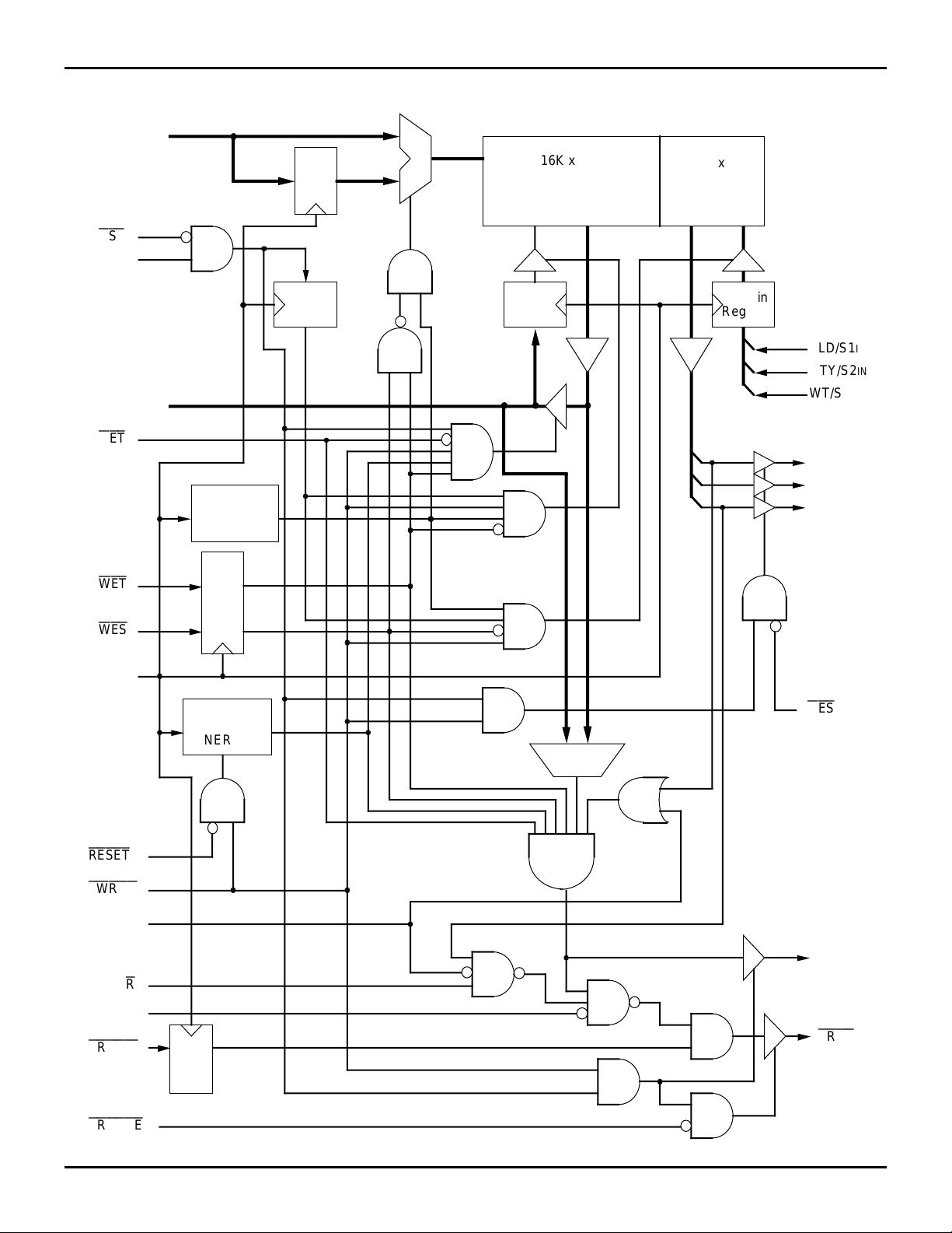
FUNCTIONAL BLOCK DIAGRAM
ADDR (0:13)
CS1
CS2
TAG (0:11)
OET
WET
WRITE
(pos) PULSE
GENERATOR
Reg
Reg
Reg
0
16K x 12
1
MEMORY
TAG BITS
Data in
Register
SA
16K x 3
MEMORY
STATUS BITS
Data in
Register
SA
VLD/S1IN
DTY/S2IN
WT/S3IN
VLD/S1
OUT
DTY/S2OUT
WT/S3OUT
WES
CLK
RESET
PWRDN
SFUNC
W/
BRDYH
BRDYIN
RESET
OES
(neg) PULSE
GENERATOR
COMPARE
MATCH
R
BRDY
Reg
BRDYOE
14.3 3
IDT71215
BiCMOS 16Kx15 CACHE-TAG RAM COMMERCIAL TEMPERATURE RANGE
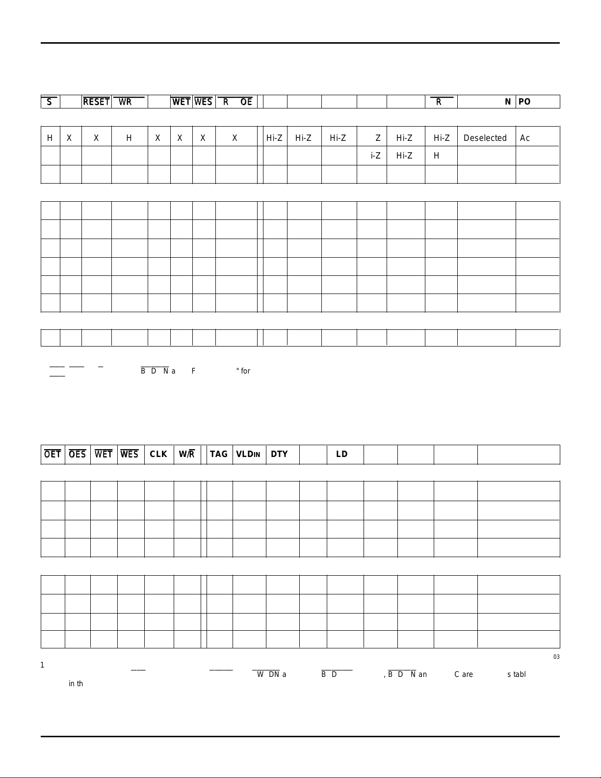
TRUTH TABLES
CHIP SELECT, RESET, AND POWER-DOWN FUNCTIONS
CS1
CS2
CS1
RESET
RESET
PWRDN
PWRDN
CLK
WET
WET
WES
WES
BRDYOE
BRDYOE
TAG VLDOUT DTYOUT WTOUT MATCH
(1, 2)
BRDY
OPERATION POWER
BRDY
CHIP SELECT FUNCTION
H X X H X X X X Hi-Z Hi-Z Hi-Z Hi-Z Hi-Z Hi-Z Deselected Active
X L X H X X X X Hi-Z Hi-Z Hi-Z Hi-Z Hi-Z Hi-Z Deselected Active
L H X H X X X X – – – – – – Selected Active
RESET FUNCTION
LH L H ↑ H H L Hi-Z L
LH L H ↑ H H H Hi-Z L
(3)
(3)
HX L H ↑ H H X Hi-Z Hi-Z Hi-Z Hi-Z Hi-Z Hi-Z Reset Status Active
XL L H ↑ H H X Hi-Z Hi-Z Hi-Z Hi-Z Hi-Z Hi-Z Reset Status Active
XX L H ↑ L X X – – – – – – Not Allowed –
XX L H ↑ X L X – – – – – – Not Allowed –
(3)
L
(3)
L
(3)
L
(3)
L
(3)
L
(3)
L
H Reset Status Active
Hi-Z Reset Status Active
POWER-DOWN FUNCTION
X X X L X H H X Hi-Z Hi-Z Hi-Z Hi-Z Hi-Z Hi-Z Power-down Standby
NOTES:
1. "H" = VIH, "L" = VIL, "X" = don't care, "–" = unrelated.
2.
OET, OES
3.
OES
, W/R, BRDYH,
is LOW.
BRDYIN
and SFUNC are "X" for this table.
3075 tbl 02
READ AND WRITE FUNCTIONS
OET
OES
WET
WES
OET
OES
WET
WES
CLK W/
(1, 2)
RRTAG VLDIN DTYIN WTIN VLDOUT DTYOUT WTOUT MATCH OPERATION
READ FUNCTION
LXHX XXD
XLXX XX – – – –D
H X X X X X Hi-Z – – – – – – D
X H X X X X – – – – Hi-Z Hi-Z Hi-Z D
OUT ––––––DOUT Read TAG I/O
OUT DOUT D OUT DOUT Read Status Bits
OUT TAG I/O Disable
OUT Status Disabled
WRITE FUNCTION
HXLX ↑XD
LXLX ↑X – – – – – – – – Not Allowed
XLXL ↑X–D
XHXL ↑X–D
NOTES:
1. "H" = VIH, "L" = VIL, "X" = don't care, "–" = unrelated.
2. This table applies when
3. D
OUT in this case is the same as DIN; that is, the input data is written through to the outputs during the write operation.
CS1
is LOW and CS2,
IN –––DOUT DOUT DOUT L Write TAG I/O
RESET
IN DIN DIN DOUT
IN DIN DIN Hi-Z Hi-Z Hi-Z L Write Status Bits
, and
PWRDN
are HIGH.
BRDYOE
(3)
, BRDYH,
DOUT
(3)
BRDYIN
(3)
DOUT
and SFUNC are "X" for this table.
L Write Status Bits
3075 tbl 03
14.3 4
IDT71215
BiCMOS 16Kx15 CACHE-TAG RAM COMMERCIAL TEMPERATURE RANGE
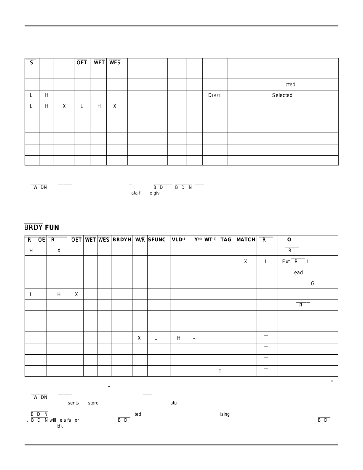
TRUTH TABLES (CONT.)
OET
OET
(1, 2, 3)
WET
WET
WES
WES
TAG VLD
(4)
DTY
(4)
(4)
WT
MATCH OPERATION
MATCH FUNCTION
CS1
CS2 SFUNC
CS1
H X X X X X Hi-Z – – – Hi-Z Deselected
X L X X X X Hi-Z – – – Hi-Z Deselected
LHXXXX ––––D
LH X L HX D
LH X H LX D
LH X X XL – D
L H L H H H TAG
L H L H H H TAG
L H H H H H TAG
NOTES: 3075 tbl 04
1. "H" = VIH, "L" = VIL, "X" = don't care, "–" = unrelated.
2. M = HIGH if TAG
3.
PWRDN
4. This column represents the stored memory cell data for the given Status bit at the selected address.
and
IN equals the memory contents at that address; M = LOW if TAGIN does not equal the memory contents at that address.
RESET
are HIGH for this table. W/R, BRDYH,
OUT – – – L Read Tag I/O
IN – – – L Write Tag I/O
IN DIN DIN L Write Status Bits
IN L – – L Invalid Data - Dedicated Status Bits
IN H – – M Match - Dedicated Status Bits
IN X – – M Match - Generic Status Bits
BRDYOE, BRDYIN, OES
OUT Selected
, and CLK are "X".
(6)
OET
OET
(1, 2, 3, 5)
WET
WET
WES
WES
BRDYH W/
RR SFUNC VLD
(4)
DTY
(4)WT(4)
TAG MATCH
BRDY
BRDY
OPERATION
BRDY
Disabled
BRDY
Input
(7)
BRDY
BRDY
BRDYOE
BRDYOE
FUNCTION
BRDYIN
BRDYIN
H X X X X X X X X – X – – Hi-Z
L L X X X X X X X – X – X L Ext
LHLXXXXXX–XDOUT L H Read TAG
LHXLXXXXX–XD
LHXXLXXXD
IN DIN DIN – L H Write Status
L H X X X H X X X – X – X H Force
IN L H Write TAG
BRDY
HIGH
L H X X X X X L L – X – L H Invalid TAG
L H X X X X H L X – H – X H Write Through
L H H H H L X L H – L TAG
L H H H H L L L H – X TAG
L H H H H L X L H – X TAG
L H H H H L X H X – X TAG
NOTES: 3075 tbl 05
1. "H" = VIH, "L" = VIL, "X" = don't care, "–" = unrelated.
2. M = HIGH if TAG
3.
PWRDN
4. This column represents the stored memory cell data for the given Status bit at the selected address.
5.
6.
7.
and
CS1
is LOW, CS2 is HIGH for this table.
BRDYIN
is a synchronous input; thus the inputs noted in the table must be applied during a rising CLK edge.
BRDYIN
will be a factor in determining the
be LOW(Valid).
IN equals the memory contents at that address; M = LOW if TAGIN does not equal the memory contents at that address.
RESET
are HIGH for this table. CLK and
BRDY
OES
are "X".
output in all cases except when BRDYH is HIGH and there is a valid MATCH. In that case,
IN M
IN M
IN M
IN M
M
M
M
M
Compare
Compare
Compare
Compare
BRDY
will
14.3 5

IDT71215
BiCMOS 16Kx15 CACHE-TAG RAM COMMERCIAL TEMPERATURE RANGE
RECOMMENDED DC
OPERATING CONDITIONS
Symbol Parameter Min. Typ. Max. Unit
VCC Supply Voltage 4.75 5.0 5.25 V
VCCQ 5V Output Buffers 4.75 5.0 5.25 V
VCCQ 3.3V Output Buffers 3.0 3.3 3.6 V
VSS Supply Ground 0 0 0 V
VIH Input High Voltage 2.2 3.0 VCC+0.3 V
IHQ I/O High Voltage 2.2 3.0 VCCQ+0.3 V
V
IL Input Low Voltage –0.5
V
NOTE: 3075 tbl 06
1. VIL (min.) = –1.5V for pulse width of less than 10ns, once per cycle.
(1)
— 0.8 V
CAPACITANCE
(TA = +25°C, f = 1.0 MHz)
Symbol Parameter
C
IN Input Capacitance VIN = 0V 5 pF
TAG TAG Input/Output VI/O = 0V 7 pF
C
Capacitance
OUT Output Capacitance VOUT = 0V 7 pF
C
NOTE: 3075 tbl 07
1. This parameter is determined by device characterization but is not production tested.
(1)
Condition Max. Unit
ABSOLUTE MAXIMUM RATINGS
(1)
Symbol Rating Value Unit
TERM Terminal Voltage with Respect –0.5 to +7.0
V
(2)
V
to GND
A Operating Temperature –0 to +70 °C
T
BIAS Temperature Under Bias –65 to +135 °C
T
STG Storage Temperature –65 to +150 °C
T
T Power Dissipation 1.7 W
P
OUT DC Output Current 20 mA
I
NOTES: 3075 tbl 08
1. Stresses greater than those listed under ABSOLUTE MAXIMUM RATINGS may cause permanent damage to the device. This is a stress rating
only and functional operation of the device at these or any other conditions
above those indicated in the operational sections of this specification is not
implied. Exposure to absolute maximum rating conditions for extended
periods may affect reliabilty.
2. V
IN should not exceed Vcc+0.5V. All pins should not exceed 7.0V.
CCQ should never exceed VCC, and VCC should never exceed
V
CCQ + 4.0V.
V
DC ELECTRICAL CHARACTERISTICS OVER THE OPERATING
TEMPERATURE AND SUPPLY VOLTAGE RANGE
(VCC = 5.0V ± 5%, VCCQ = 5.0V ± 5% OR 3.3V ± 0.3V)
Symbol Parameter Test Condition Min. Max. Unit
|I
LI| Input Leakage Current VCC = Max., VIN = 0V to VCC —5µA
|I
LO| Output Leakage Current
V
OL Output Low Voltage IOL = 4mA, VCC = Min. — 0.4 V
V
OH Output High Voltage IOH = –4mA, VCC = Min. 2.4 — V
CS1
≥ VIH, CS2 ≤ VIL, OE ≥ VIH, VCC = Max. — 5 µA
V
OUT = 0V to VCCQ, VCCQ = Max.
3075 tbl 09
DC ELECTRICAL CHARACTERISTICS OVER THE OPERATING
TEMPERATURE AND SUPPLY VOLTAGE RANGE
71215S8 71215S9 71215S10 71215S12
Symbol Parameter Test Condition Com'l. Mil. Com'l. Mil. Com'l. Mil. Com'l. Mil. Unit
CC Operating Power
I
Supply Current Outputs Open, V
ISB Standby Power
Supply Current V
ISB1 Full Standby Power
Supply Current V
NOTES: 3075 tbl 10
1. All values are maximum guaranteed values.
2.
3. f
4. V
IL, CS2 ≥ VIH.
CS1
≤ V
MAX =1/tCYC (all address inputs are cycling at fMAX). f = 0 means no address input lines are changing.
HC = VCC - 0.2V, VLC = 0.2V
PWRDN
PWRDN
PWRDN
≥ VIH 330 — 300 — 290 — 280 — mA
≤ VIL, VIN ≥ VIH or ≤ VIL 30 — 30 — 30 — 30 — mA
CC = Max., f = fMAX
≤ VIL, VIN ≥ VHC or ≤ VLC
CC = Max., f = 0
CC = Max., f = fMAX
(3)
(3)
(1, 2)
(VCC = 5.0V ± 5%)
(3)
(4)
25 — 25 — 25 — 25 — mA
14.3 6

IDT71215
BiCMOS 16Kx15 CACHE-TAG RAM COMMERCIAL TEMPERATURE RANGE
AC ELECTRICAL CHARACTERISTICS
(VCC = 5.0V ± 5%, VCCQ = 5.0V ± 5% OR 3.3V ± 0.3V, TA = 0 to 70°C)
IDT71215S8 IDT71215S9 IDT71215S10 IDT71215S12
Symbol Parameter Min. Max. Min. Max. Min. Max. Min. Max. Unit
Read Cycle
t
AAT Address Access Time Tag Bits — 10 — 11 — 12 — 14 ns
t
ACST Chip Select Access Time Tag Bits — 8 — 9 — 10 — 12 ns
(1)
CLZ
t
t
CHZ
t
OET Output Enable to Tag Bits Valid — 5 — 6 — 6 — 7 ns
OTLZ
t
t
OTHZ
t
TOH Tag Bit Hold from Address Change 2 — 2 — 2 — 2 — ns
t
OES Output Enable to Status Bits Valid — 5 — 6 — 6 — 7 ns
t
OSLZ
t
OSHZ
t
AAS Address Access Time Status Bits — 8 — 9 — 10 — 12 ns
t
ACSS Chip Select Access Time Status Bits — 6 — 7 — 8 — 10 ns
t
SOH Status Bit Hold from Address Change 2 — 2 — 2 — 2 — ns
NOTE: 3075 tbl 11
1. This parameter is guaranteed with the AC Load (Figure 3) by device characterization, but is not production tested.
Chip Select to Tag and Status Bits in Low-Z 1 — 1 — 1 — 1 — ns
(1)
Chip Select to Tag and Status Bits in High-Z 1 5161617ns
(1)
Output Enable to Tag Bits in Low-Z 0 — 0 — 0 — 0 — ns
(1)
Output Enable to Tag Bits in High-Z 1 5161617ns
(1)
Output Enable to Status Bits in Low-Z 0 — 0 — 0 — 0 — ns
(1)
Output Enable to Status Bits in High-Z 1 5161617ns
AC ELECTRICAL CHARACTERISTICS
(1)
(VCC = 5.0V ± 5%, VCCQ = 5.0V ± 5% OR 3.3V ± 0.3V, TA = 0 to 70°C)
IDT71215S8 IDT71215S9 IDT71215S10 IDT71215S12
Symbol Parameter Min. Max. Min. Max. Min. Max. Min. Max. Unit
Reset and Power Down Cycles
SR
t
t
HR
t
SRST Status Bit Reset Time — 50 — 60 — 60 — 70 ns
t
SHRS Status Bit Hold from
t
RSMI
RSMV
t
RSHZ
t
t
RSLZ
t
PDSR
t
RHPL
t
RHWL
t
PD
t
PU
PDHZ
t
PDLZ
t
PUV
t
WHPL
t
t
PUWL
NOTES: 3075 tbl 12
1. Power-down mode is intended to be used during extended time periods of device inactivity.
2. This parameter is guaranteed with the AC Load (Figure 3) by device characterization, but is not production tested.
RESET
Set-up Time 4 — 4 — 4 — 4 — ns
RESET
Hold Time 1 — 1 — 1 — 1 — ns
RESET
LOW 2 —2—2—2—ns
RESET
LOW to MATCH and
RESET
HIGH to MATCH and
(2)
RESET
LOW to TAG High-Z — 9 — 10 — 10 — 12 n s
(2)
RESET
HIGH to TAG Low-Z — 90 — 100 — 100 — 110 ns
PWRDN
RESET
RESET
(2)
PWRDN
(2)
PWRDN
(2)
PWRDN
(2)
PWRDN
PWRDN
(2)
WET
PWRDN
Set-up to
HIGH to
HIGH to
RESET
PWDRN
WET
and
LOW to Low Power Mode — 50 — 50 — 50 — 50 ns
HIGH to Active Power Mode 0 — 0 — 0 — 0 — ns
LOW to Outputs in High-Z — 9 — 10 — 10 — 12 ns
HIGH to Outputs in Low-Z 0 — 0 — 0 — 0 — ns
HIGH to Outputs Valid — 50 — 50 — 50 — 50 ns
and
WES
HIGH to
HIGH to
WET
BRDY
Invalid — 9 — 10 — 10 — 12 ns
BRDY
Valid — 110 — 120 — 120 — 130 ns
LOW 30 — 30 — 30 — 30 — ns
LOW 1 —1—1—1—CLK
WES
LOW 90 — 95 — 95 — 105 — ns
PWRDN
and
LOW 5 —5—5—5—ns
WES
Active 50 — 50 — 50 — 50 — ns
14.3 7

IDT71215
BiCMOS 16Kx15 CACHE-TAG RAM COMMERCIAL TEMPERATURE RANGE
AC ELECTRICAL CHARACTERISTICS
(1)
(VCC = 5.0V ± 5%, VCCQ = 5.0V ± 5% OR 3.3V ± 0.3V, TA = 0 to 70°C)
IDT71215S8 IDT71215S9 IDT71215S10 IDT71215S12
Symbol Parameter Min. Max. Min. Max. Min. Max. Min. Max. Unit
Write Cycle and Clock Parameters
t
CYC Clock Cycle Time 15 — 15 — 15 — 16.6 — ns
(2, 3)
t
CH
(2, 3)
t
CL
t
S
t
H
t
SA Address Set-up Time 3 — 3 — 3 — 3 — ns
t
HA Address Hold Time 1 — 1 — 1 — 1 — ns
t
WMI CLK HIGH Write to MATCH and
t
CKLZ
(4)
t
CTV
t
CSV
t
CSH
t
WHPL
t
PUWL
NOTES: 3075 tbl 14
1. All Write cycles are synchronous and referenced from rising CLK.
2. This parameter is measured as a HIGH time above 2.0V and a LOW time below 0.8V.
3. This parameter is guaranteed with the AC Load (Figure 3) by device characterization, but is not production tested.
4. Addresses are stable prior to CLK transition HIGH.
Clock Pulse HIGH 4.5 — 4.5 — 4.5 — 5 — ns
Clock Pulse LOW 4.5 — 4.5 — 4.5 — 5 — ns
WET, WES
WET, WES
3)
(
CLK HIGH Read to Outputs in Low-Z 1.5 — 1.5 — 1.5 — 1.5 — ns
, Chip Select, and Input Data Set-up Time 3 — 3 — 3 — 3 — ns
, Chip Select, and Input Data Hold Time 1 — 1 — 1 — 1 — ns
BRDY
Invalid — 6 — 7 — 7 — 8 ns
CLK HIGH Read to Tag Bits Valid — 9 — 10 — 10 — 12 ns
(4)
CLK HIGH Write to Status Outputs Valid — 8 — 9 — 9 — 10 ns
(3)
Status Output Hold from CLK HIGH Write 0 — 0 — 0 — 0 — ns
WET
and
WES
PWRDN
HIGH to
HIGH to
WET
PWRDN
and
LOW 5—5—5 —5—ns
WES
Active 50 — 50 — 50 — 50 — ns
14.3 8

IDT71215
BiCMOS 16Kx15 CACHE-TAG RAM COMMERCIAL TEMPERATURE RANGE
AC ELECTRICAL CHARACTERISTICS
(VCC = 5.0V ± 5%, VCCQ = 5.0V ± 5% OR 3.3V ± 0.3V, TA = 0 to 70°C)
IDT71215S8 IDT71215S9 IDT71215S10 IDT71215S12
Symbol Parameter Min. Max. Min. Max. Min. Max. Min. Max. Unit
MATCH and
t
ADM Address to MATCH Valid — 8 — 9 — 10 — 12 ns
t
DAM Data Input to MATCH Valid — 8 — 9 — 10 — 12 ns
t
CSM Chip Select to MATCH Valid — 8 — 9 — 10 — 12 ns
(1)
CMLZ
t
(1)
t
CMHZ
t
MHA MATCH Valid Hold from Address 2 — 2 — 2 — 2 — ns
t
MHD MATCH Valid Hold from Data 2 — 2 — 2 — 2 — ns
t
BHA
t
BHD
t
ADB Address to
t
DAB Data Input to
t
CSB Chip Select LOW to
t
OEBV
(1)
t
OBLZ
(1)
t
OBHZ
t
BYFH BRDYH HIGH to Force
t
BYHV BRDYH LOW to
t
SB
t
HB
t
BIBL CLK HIGH
t
BIBV CLK HIGH
t
OEMI
t
OEMV
2)
(
t
WRBH
(2)
t
WRBV
t
WMI CLK HIGH Write to MATCH and
(3)
t
WMV
NOTES: 3075 tbl 15
1. This parameter is guaranteed with the AC Load (Figure 3) by device characterization, but is not production tested.
2. These parameters only apply when SFUNC is LOW and the internal WT bit is HIGH.
ADM, tDAM, tCSM and tADB, tDAB, tCSB must also be satisfied.
3. t
BRDY
Cycles
BRDY
Chip Select to MATCH in Low-Z 1 — 1 — 1 — 1 — ns
Chip Select to MATCH in High-Z 1 5 1 6 1 6 1 7 ns
BRDY
Valid Hold from Address 2 — 2 — 2 — 2 — ns
BRDY
Valid Hold from Data 2 — 2 — 2 — 2 — ns
BRDY
Valid — 9 — 10 — 11 — 13 ns
BRDY
Valid — 9 — 10 — 11 — 13 ns
BRDY
Valid — 9 — 10 — 11 — 13 ns
BRDYOE
BRDYOE
BRDYOE
BRDYIN
BRDYIN
OET
OET
W/R HIGH to
W/R LOW to
CLK HIGH Read to MATCH and
LOW to
LOW to
HIGH to
BRDY
Valid — 6 — 6 — 7 — 8 ns
BRDY
in Low-Z 0 — 0 — 0 — 0 — ns
BRDY
in High-Z 1 5 1 6 1 6 1 7 ns
BRDY
HIGH — 5 — 5 — 5 — 6 ns
BRDY
Valid — 5 — 5 — 5 — 6 ns
Set-up Time 4 — 4 — 4 — 4 — ns
Hold Time 1.5 — 1.5 — 1.5 — 1.5 — ns
BRDYIN
BRDYIN
LOW to MATCH and
HIGH to MATCH and
LOW to
HIGH to
BRDY
HIGH — 6 — 7 — 7 — 8 ns
BRDY
Valid — 6 — 7 — 7 — 8 ns
BRDY
LOW — 6 — 6 — 7 — 8 ns
BRDY
Valid — 6 — 6 — 7 — 8 ns
BRDY
Invalid — 6 — 7 — 7 — 8 ns
BRDY
Valid — 7 — 8 — 8 — 10 ns
BRDY
Invalid — 7 — 7 — 7 — 8 ns
BRDY
Valid — 8 — 9 — 10 — 12 ns
14.3 9

IDT71215
BiCMOS 16Kx15 CACHE-TAG RAM COMMERCIAL TEMPERATURE RANGE
AC TEST CONDITIONS
Input Pulse Levels GND to 3.0V
Input Rise/Fall Times 3ns
Input Timing Reference Levels 1.5V
Output Timing Reference Levels 1.5V
AC Test Load See Figs. 1, 2, 3, & 4
3075 tbl 16
AC TEST LOADS
Outputs
347 Ω
CCQ
V
893
30pF *
Figure 1. AC Test Load
CCQ
V
Ω
893
Ω
Tag I/O
347 Ω
3075 drw 03
Figure 2. Tag I/O AC Test Load
* Including scope and jig capacitance
50pF *
3075 drw 04
Tag I/O
and
Outputs
347 Ω
Figure 3. AC Test Load
(for t
HZ and tLZ parameters )
* Including scope and jig capacitance
V
CCQ
893
5pF*
6
5
Ω
4
3
∆t
(Typical, ns)
2
3075 drw 05
1
20 30 50 100
80
∆ Capacitance (pF)
3075 drw 06
Figure 4. Lumped Capacitance Load, Typical Derating
14.3 10

IDT71215
BiCMOS 16Kx15 CACHE-TAG RAM COMMERCIAL TEMPERATURE RANGE
TIMING WAVEFORMS OF WRITE AND READ CYCLES
Valid
Output
Valid
Output
Valid
Valid
3075 drw 07
TAG
READ
VALID
VALID
tAAT
tAAT
tTOH
tACST
tCHZ(1)
tS
tAAS
tOET
tCLZ(1)
tOTLZ(1)
tOTHZ(1)
tSOH
tACSS
tCHZ(1)
tCLZ(1)
Valid
Valid Output
tCTV
tH
tCKLZ(1)
tAAS
tSOH
Valid
TAG WRITE
STATUS WRITE
CLK
VALID
tS
A (0:13)
tCSV
tH
tH
tH
Valid
tS
Valid Input
tS
tCSH
NOTE:
1. Transition is measured ±200mV from steady state.
OUT
WT
CS1
CS2
WET
OET
WES
IN
VLD
WTIN
DTYIN
VLDOUT
DTYOUT
TAG (0:11)
14.3 11

IDT71215
BiCMOS 16Kx15 CACHE-TAG RAM COMMERCIAL TEMPERATURE RANGE
TIMING WAVEFORMS OF MATCH AND
BRDY
BRDY
FUNCTIONS
tCMLZ(1)
tOBLZ(1)
tOEMV
tCSB
tOEBV
tCSM
tOEMI
Valid
3075 drw 08
tOBHZ(1)
Valid
tCMHZ(1)
Valid
Valid
Valid
tWMV
tS
tH
tWMI
tS
tH
tS
tH
tS
tBYHV
tWMV
tWMI
tBYFH
Valid
Valid
Valid BRDY
Valid
MATCH Valid
CLK
tADB
tADM
Valid Address
A (0:13)
tMHA
tBHA
tDAB
Valid Match Data
TAG (0:11)
tDAM
tMHD
tBHD
CS1
CS2
Valid
WES
14.3 12
WET
OET
BRDYH
BRDY
BRDYOE
Valid
MATCH
NOTE:
1. Transition is measured ±200mV from steady state.

IDT71215
BiCMOS 16Kx15 CACHE-TAG RAM COMMERCIAL TEMPERATURE RANGE
TIMING WAVEFORMS OF
CLK
tSR
RESET
tPDSR
PWRDN
VLDOUT
DTYOUT
WT
OUT
WES
WET
BRDY
MATCH
TAG (0:11)
NOTE:
1. Transition is measured ±200mV from steady state.
tS
RESET
RESET
tSHRS
tRSMI
tRSHZ(1)
FUNCTION
tHR
tSRST
tRHWL
tRSMV
VALID
VALID
tRSLZ(1)
3075 drw 09
CLOCK TIMING WAVEFORM
CLK
TIMING WAVEFORMS OF
CLK
BRDYIN
W/
R
BRDY
2.0V 2.0V
tWRBH tWRBV
BRDY
Valid
BRDY
BRDY
Applies when SFUNC is LOW, and the internal WT bit is HIGH
AND W/
tCYCtCH tCL
RR SIGNAL
tSB tHB
BRDY
0.8V
tBIBL tBIBV
Valid
0.8V
3075 drw 10
3075 drw 11
14.3 13

IDT71215
BiCMOS 16Kx15 CACHE-TAG RAM COMMERCIAL TEMPERATURE RANGE
TIMING WAVEFORMS OF
OES
VLDOUT
DTYOUT
WTOUT
NOTE:
1. Transition is measured ±200mV from steady state.
OES
FUNCTION
OES
tOSHZ(1)
Valid Output
TIMING WAVEFORMS OF POWER DOWN FUNCTION
PWRDN
tWHPL tPUWL
CLK
tRHPL
RESET
tS tS
tOES
tOSLZ(1)
Valid Output
3075 drw 12
WET, WES
TAG (0:11)
OUT
VLD
DTYOUT
OUT
WT
BRDY
MATCH
I
CC
NOTE:
1. Transition is measured ±200mV from steady state.
ISB
ORDERING INFORMATION
IDT 71215 PFXX
Device Type Package
S
Power Speed
tPDHZ(1)
tPDLZ(1)
tPD tPU
PF Plastic Thin Quad Flatpack (PN80-1)
tPUV
Valid TAG out
Valid Status out
BRDY
Valid
MATCH Valid
3075 drw 13
8
9
10
12
14.3 14
Speed in nanoseconds
3075 drw 14
 Loading...