


查询IDT70V631S供应商
HIGH-SPEED 3.3V 256K x 18
ASYNCHRONOUS DUAL-PORT
STATIC RAM
Features
◆◆
◆
◆◆
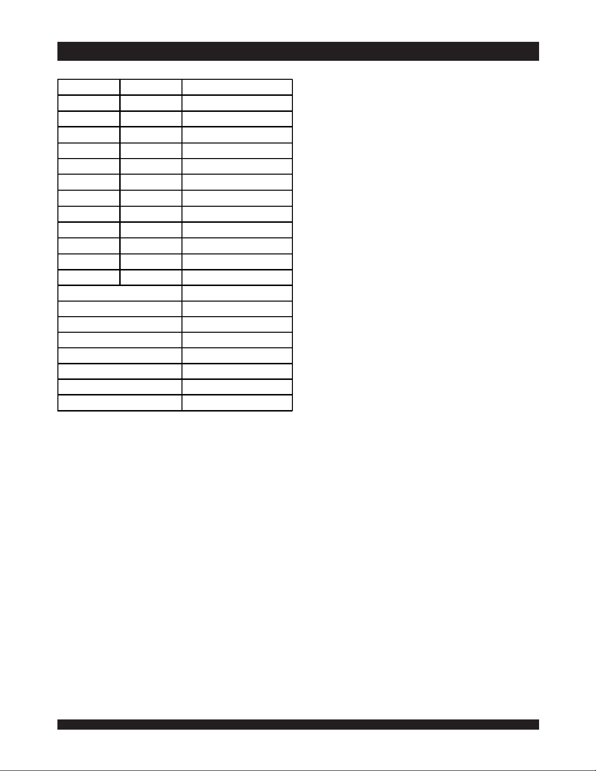
True Dual-Port memory cells which allow simultaneous
access of the same memory location
◆◆
◆
◆◆
High-speed access
– Commercial: 10/12/15ns (max.)
– Industrial: 12ns (max.)
◆◆
◆
◆◆
Dual chip enables allow for depth expansion without
external logic
◆◆
◆
◆◆
IDT70V631 easily expands data bus width to 36 bits or
more using the Master/Slave select when cascading more
than one device
◆◆
◆
◆◆
M/S = VIH for BUSY output flag on Master,
M/S = VIL for BUSY input on Slave
◆◆
◆
◆◆
Busy and Interrupt Flags
◆◆
◆
◆◆
On-chip port arbitration logic
◆◆
◆
◆◆
Full on-chip hardware support of semaphore signaling
between ports
Functional Block Diagram
UB
L
LB
L
IDT70V631S
◆◆
◆
◆◆
Fully asynchronous operation from either port
◆
Separate byte controls for multiplexed bus and bus
matching compatibility
◆◆
◆
◆◆
Supports JTAG features compliant to IEEE 1149.1
– Due to limited pin count, JTAG is not supported on the
128-pin TQFP package.
◆◆
◆
◆◆
LVTTL-compatible, single 3.3V (±150mV) power supply for
core
◆◆
◆
◆◆
LVTTL-compatible, selectable 3.3V (±150mV)/2.5V (±100mV)
power supply for I/Os and control signals on each port
◆◆
◆
◆◆
Available in a 128-pin Thin Quad Flatpack, 208-ball fine
pitch Ball Grid Array, and 256-ball Ball Grid Array
◆◆
◆
◆◆
Industrial temperature range (–40°C to +85°C) is available
for selected speeds
UB
R
LB
R
R/
W
L
CE
0L
CE
1L
OE
L
I/O0L- I/O
17L
A
BUSY
SEM
INT
17L
A
0L
L
L
L
Address
Decoder
CE
0L
CE
1L
OE
R/W
TDI
TDO
NOTES:
1. BUSY is an input as a Slave (M/S=V
IL) and an output when it is a Master (M/S=VIH).
2. BUSY and INT are non-tri-state totem-pole outputs (push-pull).
©2003 Integrated Device Technology, Inc.
R/
W
B
B
B
E
1
L
256K x 18
MEMORY
ARRAY
INTERRUPT
LOGIC
M/S
B
E
E
1
0
R
R
Dout0-8_R
Dout9-17_R
Din_R
ADDR_R
R/W
Address
Decoder
OE
R
CE
0R
CE
R
1R
BUSY
SEM
INT
E
0
L
Dout0-8_L
Dout9-17_L
Din_L
ADDR_L
L
L
ARBITRATION
SEMAPHORE
R
CE
0R
CE
1R
R
OE
I/O0R-I/O
17R
A
17R
A
0R
R
R
R
TMS
JTAG
TCK
TRST
5622 drw 01
OCTOBER 2003
1
DSC-5622/5

IDT70V631S
High-Speed 3.3V 256K x 18 Asynchronous Dual-Port Static RAM Industrial and Commercial Temperature Ranges
Description
The IDT70V631 is a high-speed 256K x 18 Asynchronous Dual-Port
Static RAM. The IDT70V631 is designed to be used as a stand-alone
4608K-bit Dual-Port RAM or as a combination MASTER/SLAVE DualPort RAM for 36-bit-or-more word system. Using the IDT MASTER/
SLAVE Dual-Port RAM approach in 36-bit or wider memory system
applications results in full-speed, error-free operation without the need for
additional discrete logic.
This device provides two independent ports with separate control,
address, and I/O pins that permit independent, asynchronous access for
reads or writes to any location in memory. An automatic power down
feature controlled by the chip enables (either CE
0 or CE1) permit the
on-chip circuitry of each port to enter a very low standby power mode.
The 70V631 can support an operating voltage of either 3.3V or 2.5V
on one or both ports, controlled by the OPT pins. The power supply for
the core of the device (VDD) remains at 3.3V.
Pin Configurations
09/3 0/03
A
B
C
D
E
F
G
H
J
K
L
M
I/O
9L
NC V
V
DDQ L
NC
I/O
11L
V
DDQ L
NC
V
DD
V
DDQL
I/O
14RVSS
NC I/O
V
DDQ L
21
NC V
SS
I/O
9R
V
SS
NC
11R
I/O
V
SS
NC
V
DD
14LVDDQR
NC
(1,2,3,4)
9876543
10
DD
A
SS
TDO
NC
NC
TDI
A
17L
V
DD
V
DDQ R
I/O
10L
V
DDQR
NC
I/O
12L
V
DDQR
VSSV
I/O
13R
15RVSS
I/O
NC
A
15LA11LA7L
NC V
I/O
10R
SS
V
NC
I/O
12R
SS
V
SS
I/O
13L
12L
A
16L
A
13L
A
14L
8L
A
9L
NC
A
10L
UB
L
LB
L
70V631BF
BF-208
208-Ball BGA
Top V iew
V
NCA
V
SS
CE
0L
CE
1L
V
SS
V
DD
OE
(5)
(6)
11
INT
L
SEM
L
A
5L
BUSY
L
A
6
L
R/
W
L
NC
A
L
3L
1412 13
A
A
4L
1L
A
V
A
2L
V
NC
DD
I/O6LNC V
V
NC V
V
V
I/O
NC
V
15
0L
V
DDQR
SS
I/O
8R
DD
V
DDQL
SS
I/O
6R
DDQL
DD
NC
V
DD
SS
V
DDQL
3R
I/O
3L
SS
NC
1716
A
V
SS
NCOPT
L
I/O
8L
NC
B
V
SS
NC
I/O
7L
SS
NC
I/O
5L
V
SS
V
SS
I/O
4R
V
SS
I/O
2R
V
I/O
I/O
V
I/O
V
NC
DDQR
NC
DDQR
V
DDQR
C
7R
D
E
F
G
5R
H
J
SS
K
L
4L
M
NC
V
SS
NC I/O
N
I/O
16R
I/O
SS
V
NC I/O
V
SS
16LVDDQR
NC I/O
17LVDDQL
NC
P
R
T
U
15L
DD
NC
TCK
17R
TMS
V
DD
NC
TRST
A
17R
NC
A
15R
A
16RA12RA8R
A
13RA9R
A
14RA10R
A
11RA7R
NC
UB
R
LB
R
V
NC
V
SS
CE
0R
V
SS
CE
1R
V
DD
OE
R
SEM
BUSY
R/
M/
INT
R
R
A
5R
R
A
6R
W
R
A
3R
S
I/O
1R
V
DDQL
NC I/O
V
SS
V
V
SS
NC
V
DD
OPTRNC I/O
1L
DDQL
A
4R
A
1R
A
2R
0R
A
NOTES:
DD pins must be connected to 3.3V power supply.
1. All V
DDQ pins must be connected to appropriate power supply: 3.3V if OPT pin for that port is set to VIH (3.3V) and 2.5V if OPT pin for that port is
2. All V
3. All V
IL (0V).
set to V
SS pins must be connected to ground.
4. Package body is approximately 15mm x 15mm x 1.4mm with 0.8mm ball pitch.
5. This package code is used to reference the package diagram.
6. This text does not indicate orientation of the actual part-marking.
2
NC
V
SS
I/O0RV
V
SS
I/O
2L
NC
DDQR
NC
0L
5622 tbl 02b
N
P
R
T
U

IDT70V631S
High-Speed 3.3V 256K x 18 Asynchronous Dual-Port Static RAM Industrial and Commercial Temperature Ranges
Pin Configurations
09/30/03
A
14L
A
15L
A
16L
A
17L
IO
9L
IO
9R
V
DDQL
V
SS
IO
10L
IO
10R
V
DDQR
V
SS
IO
11L
IO
11R
IO
12L
IO
12R
V
DD
V
DD
V
SS
V
SS
IO
13R
IO
13L
IO
14R
IO
14L
IO
15R
IO
15L
V
DDQL
V
SS
IO
16R
IO
16L
V
DDQR
V
SS
IO
17R
IO
17L
A
17R
A
16R
A
15R
A
14R
(1,2,3,4,7)
L
3
1
A
8
2
1
1
2
3
4
5
6
7
8
9
10
11
12
13
14
15
16
17
18
19
20
21
22
23
24
25
26
27
28
29
30
31
32
33
34
35
36
37
9
38
3
L
L
2
1
1
1
A
A
6
7
2
2
1
1
1
0
4
4
(con't.)
L
0
1
A
5
2
1
2
4
L
L
L
L
B
9
8
7
A
A
A
U
1
2
3
4
2
2
2
2
1
1
1
1
3
4
5
4
4
4
L
L
1
0
D
L
E
E
D
B
L
C
C
V
7
9
8
0
1
1
1
2
1
1
1
1
L
M
D
S
S
E
D
S
S
V
V
V
S
4
3
5
6
1
1
1
1
1
1
1
1
70V631PRF
PK-128
(5)
128-Pin TQFP
Top View
8
9
7
6
4
4
4
4
0
5
(6)
4
2
3
1
5
5
5
5
L
Y
L
L
L
S
W
T
E
/
U
N
O
R
B
I
0
9
2
1
1
0
1
1
1
1
1
1
6
7
5
5
5
5
L
L
L
L
C
6
N
A
8
7
0
0
1
1
8
9
5
5
L
5
4
3
2
A
A
A
A
5
4
3
6
0
0
0
0
1
102
1
1
1
101
100
99
98
97
96
95
94
93
92
91
90
89
88
87
86
85
84
83
82
81
80
79
78
77
76
75
74
73
72
71
70
69
68
67
66
4
2
3
0
1
6
6
65
6
6
6
A
1L
A
0L
OPT
V
SS
IO
IO
NC
V
SS
V
DDQL
IO
7L
IO
7R
V
SS
V
DDQR
IO
IO
IO
IO
V
DD
V
DD
V
SS
V
SS
IO
IO
IO
IO
IO
IO
V
SS
V
DDQL
IO
IO
V
SS
V
DDQR
IO
IO
OPT
A
0R
A
1R
L
8L
8R
6L
6R
5L
5R
4R
4L
3R
3L
2R
2L
1R
1L
0R
0L
R
.
R
R
3
2
1
1
A
A
R
R
R
R
9
8
1
0
1
1
A
A
A
A
R
R
R
R
7
1
B
B
A
E
L
U
C
S
S
R
R
D
D
R
0
S
D
D
E
V
V
V
C
R
S
E
M
W
V
/
O
E
R
S
R
R
R
R
R
R
S
/
6
T
Y
A
M
S
N
I
U
B
R
2
A
5622 drw 02a
5
4
3
A
A
A
NOTES:
DD pins must be connected to 3.3V power supply.
1. All V
DDQ pins must be connected to appropriate power supply: 3.3V if OPT pin for that port is set to VIH (3.3V) and 2.5V if OPT pin for that port is
2. All V
3. All V
IL (0V).
set to V
SS pins must be connected to ground.
4. Package body is approximately 14mm x 20mm x 1.4mm.
5. This package code is used to reference the package diagram.
6. This text does not indicate orientation of the actual part-marking.
7. Due to the restricted number of pins, JTAG is not supported in the PK-128 package.
3

IDT70V631S
High-Speed 3.3V 256K x 18 Asynchronous Dual-Port Static RAM Industrial and Commercial Temperature Ranges
Pin Configuration
(1,2,3,4)
(con't.)
09/30/03
A3
A2
A1
NC
B1
NC
C1
NC
D1
NC
E1
I/O
10R
F1
I/O
11L
G1
NC
H1
NCH2I/O
J1
I/O
13L
K1
NC
L1
I/O
15L
M1
I/O
16R
N1
NCN2I/O
P1
NCP2I/O
R1
B2
C2
I/O
D2
I/O
E2
I/O
F2
G2
J2
I/O
K2
L2
M2
I/O
TDI
B3
NC
C3
9L
D3
9R
E3
10L
NCF3I/O
G3
NC
I/O
H3
12R
J3
14R
I/O
K3
NC
I/O
L3
I/O
NC
M3
16L
N3
17R
P3
17L
NC
TDO
V
SS
NC
NCE4V
11R
12L
NCH4V
13R
14L
15R
NCM4V
NC
TMSP4A
NCR2NCR3TRSTR4NC
T2
T1
NC
TCKT3NC
A4
A
B4
C4
D4
F4
V
G4
V
J4
V
K4
V
L4
V
N4
T4
17L
NC
A
16L
V
DD
DDQL
DDQL
DDQR
DDQR
DDQL
DDQL
DDQR
DDQR
V
DD
16R
A
17R
A5
A
B5
C5
D5
V
E5
F5
G5
H5
J5
K5
L5
M5
N5
V
P5
A
R5
A
T5
14L
A
15L
A
13L
DDQL
V
DD
V
DD
V
V
SS
V
V
V
V
DDQR
13R
15R
A
14R
SS
SS
SS
DD
DD
A6
A
B6
C6
D6
V
E6
F6
G6
H6
J6
K6
L6
M6
N6
V
P6
R6
A
T6
11L
A
12L
A
10L
DDQL
V
DD
V
SS
V
SS
V
SS
V
SS
V
SS
V
SS
V
DD
DDQR
A
10R
12R
A
11R
70V631BC
BC-256
256-Pin BGA
Top View
A7
A8
NC
A
8L
B7
B8
A
9L
UB
C8
C7
D7
V
E7
F7
G7
H7
J7
K7
L7
M7
N7
V
P7
R7
A
T7
A
7L
DDQR
V
SS
V
SS
V
SS
V
SS
V
SS
V
SS
V
SS
V
SS
DDQL
A
7R
9R
A
8R
NC
D8
V
DDQR
E8
V
F8
V
G8
V
H8
V
J8
V
K8
V
L8
V
M8
V
N8
V
DDQL
P8
NCP9LB
R8
UB
T8
NC
(5)
(6)
A13
A10
OE
B10
R/W
C10
SEM
D10
V
DDQL
E10
V
F10
V
G10
V
H10
V
J10
V
K10
V
L10
V
M10
V
N10
V
DDQR
P10
SEM
R10
R/W
T10
OE
A11
INT
L
B11
L
C11
BUSY
L
D11
V
E11
SS
F11
SS
G11
SS
H11
SS
J11
SS
K11
SS
L11
SS
M11
SS
N11
V
P11
R
BUSY
R11
R
T11
INT
R
NC
DDQR
V
DD
V
SS
V
SS
V
SS
V
SS
V
SS
V
SS
V
DD
DDQL
M/S
A
5L
L
B12
A
4L
C12
A
6L
L
D12
V
DDQR
E12
V
DD
F12
V
DD
G12
V
SS
H12
V
SS
J12
V
SS
K12
V
SS
L12
V
DD
M12
V
DD
N12
V
DDQL
P12
A
6R
R
R12
A
4R
T12
R
A
5R
A9
CE
1L
B9
CE
0L
L
C9
LB
L
D9
V
DDQL
E9
SS
V
SS
F9
V
SS
SS
G9
SS
V
SS
H9
SS
V
SS
J9
SS
V
SS
K9
SS
V
SS
L9
SS
V
SS
M9
SS
V
SS
N9
V
DDQR
R
R9
R
CE
0R
T9
CE
1R
A12
B13
C13
D13
E13
V
F13
V
G13
V
H13
V
J13
V
K13
V
L13
V
M13
V
N13
P13
R13
T13
A
2L
A
1L
A
3L
V
DD
DDQR
DDQR
DDQL
DDQL
DDQR
DDQR
DDQL
DDQL
V
DD
A
3R
A
1R
A
2R
A14
B14
C14
OPT
D14
E14
F14
I/O
G14
I/O
H14
J14
I/O
K14
L14
I/O
M14
I/O
N14
NC
P14
R14
OPT
T14
A
A
NC
NC
NC
NC
NC
NC
0L
0R
A15
B15
C15
L
D15
E15
F15
6R
G15
5L
H15
J15
4R
K15
L15
2L
M15
1R
N15
P15
R15
R
T15NCT16
NC
NC
NC
NC
I/O
NC
NC
NC
I/O
NC
NC
I/O
I/O
NC
NC
A16
NC
B16
NC
C16
I/O
8L
D16
I/O
8R
E16
I/O
7R
7L
F16
I/O
6L
G16
NC
H16
I/O
5R
J16
I/O
4L
3R
K16
I/O
3L
L16
I/O
2R
M16
NC
1L
N16
NC
0R
P16
I/O
0L
R16
NC
,
NC
NOTES:
DD pins must be connected to 3.3V power supply.
1. All V
DDQ pins must be connected to appropriate power supply: 3.3V if OPT pin for that port is set to VIH (3.3V), and 2.5V if OPT pin for that port is
2. All V
3. All V
IL (0V).
set to V
SS pins must be connected to ground supply.
4. Package body is approximately 17mm x 17mm x 1.4mm, with 1.0mm ball-pitch.
5. This package code is used to reference the package diagram.
6. This text does not indicate orientation of the actual part-marking.
4
5622 drw 02c
,
IDT70V631S
High-Speed 3.3V 256K x 18 Asynchronous Dual-Port Static RAM Industrial and Commercial Temperature Ranges
Pin Names
Left Port Right Port Names
0L
CE
R/W
OE
L
0L
- A
A
0L
I/O
SEM
INT
BUSY
UB
L
L
LB
,
L
- I/O
L
L
CE
L
17 L
DD Q L
V
OPT
1L
17L
CE
0R
,
CE
1R
R/ W
R
OE
R
A0R - A
17R
I/O0R - I/O
17R
SEM
R
INT
R
BUSY
R
UB
R
LB
R
V
DDQR
L
OPT
M/S Master or Slave Select
DD
V
V
SS
TDI Test Data Inpu t
TDO Tes t Data Outp ut
TCK Test Logic Clock (10MHz)
TMS Test Mode Select
TRST
Chip Enables
Read/Write E nab le
Output Enable
Address
Data Input/ Outp ut
Semaphore Enable
Inte rrupt Flag
Busy Flag
Uppe r Byte Se lect
Lower Byte Sele ct
Po wer (I/O Bus) (3.3V or 2.5V)
R
Op tio n for se le c ting V
Po wer (3.3V)
Ground (0V)
Re se t (In iti al ize TAP Control le r)
(1)
(1,2)
DDQX
(1 )
NOTES:
DD, OPTX, and VDDQX must be set to appropriate operating levels prior to
1. V
applying inputs on I/O
X selects the operating voltage levels for the I/Os and controls on that port.
2. OPT
X is set to VIH (3.3V), then that port's I/Os and controls will operate at 3.3V
If OPT
levels and V
DDQX must be supplied at 3.3V. If OPTX is set to VIL (0V), then that
port's I/Os and controls will operate at 2.5V levels and V
X.
DDQX must be supplied
at 2.5V. The OPT pins are independent of one another—both ports can operate
at 3.3V levels, both can operate at 2.5V levels, or either can operate at 3.3V
with the other at 2.5V.
56 22 tbl 01
5

IDT70V631S
High-Speed 3.3V 256K x 18 Asynchronous Dual-Port Static RAM Industrial and Commercial Temperature Ranges
Byte 0
I/O
0-8
(1)
MODE
Truth Table I—Read/Write and Enable Control
Byte 1
9-1 7
I/O
OE SEM CE
CE
0
1
UB LB
R/W
X H H X X X X High-Z High-Z Deselected–Power Down
X H X L X X X High-Z High-Z Deselected–Power Down
X H L H H H X High-Z Hig h-Z Both Bytes De se le cte d
IN
IN
OUT
OUT
Write to Byte 0 Only
Write to Both Bytes
Read Byte 0 Only
Read Both Bytes
XHLHHLLHigh-Z D
XHLHLHL D
XHLHL LL D
IN
IN
High-Z Write to Byte 1 Only
D
LHLHHLHHigh-ZD
LHLHLHHD
LHLHLLHD
OUT
OUT
High-Z Re ad Byte 1 Only
D
H H L H L L X High-Z High-Z Outputs Disabled
NOTE:
1. "H" = V
IH, "L" = VIL, "X" = Don't Care.
5622 tbl 0 2
Truth Table II – Semaphore Read/Write Control
(1)
Inputs
CE
R/W
OE UB LB SEM
HHLLLLDATA
H
↑
XXL L X DATAINWrite I/O0 into Semaphore Flag
LXXXX L
NOTE:
1. There are eight semaphore flags written to I/O
2. CE = L occurs when CE
0 = VIL and CE1 = VIH.
0 and read from all the I/Os (I/O0-I/O17). These eight semaphore flags are addressed by A0-A2.
3. Each byte is controlled by the respective UB and LB. To read data UB and/or LB = V
Outputs
1-1 7
I/O
OUT
DATA
______ ______
I/O
0
OUT
Read Data in Se map ho re Flag
Not Al lowed
IL.
(1)
Mode
(3)
5622 tbl 03
6

IDT70V631S
High-Speed 3.3V 256K x 18 Asynchronous Dual-Port Static RAM Industrial and Commercial Temperature Ranges
Recommended Operating
Temperature and Supply Voltage
Ambient
Grade
Commercial 0OC to +70OC0V3.3V
Industrial -40
NOTE:
1. This is the parameter T
Absolute Maximum Ratings
Symbol Rating Commercial
(2)
V
TE R M
Terminal Voltage
with Res pect to
GND
T
BIAS
Te m p e r a tu r e
Unde r Bias
T
STG
Storage
Te m p e r a tu r e
I
OUT
DC Output Current 50 mA
NOTES:
1. Stresses greater than those listed under ABSOLUTE MAXIMUM RATINGS may
cause permanent damage to the device. This is a stress rating only and functional
operation of the device at these or any other conditions above those indicated
in the operational sections of this specification is not implied. Exposure to absolute
maximum rating conditions for extended periods may affect reliability.
TERM must not exceed VDD + 150mV for more than 25% of the cycle time or
2. V
4ns maximum, and is limited to
Capacitance
(TA = +25°C, F = 1.0MHZ) TQFP ONLY
Symbol Parameter Conditions
Temperature GND V
O
C to +85OC0V3.3V + 150mV
A. This is the "instant on" case temperature.
(1)
& Industrial
-0.5 to +4.6 V
-55 to +125
-65 to +150
< 20mA for the period of VTERM > VDD + 150mV.
(1)
(2 )
(1)
DD
+
150mV
5622 tbl 04
Unit
o
C
o
C
56 22 tb l 05
Max. Unit
Recommended DC Operating
Conditions with V
Symbol Parameter Min. Typ. Max. Unit
DD
Core Sup ply Voltage 3.15 3. 3 3.45 V
V
DDQ
I/O Supply Voltage
V
SS
Ground 0 0 0 V
V
Inp ut High Vol tage
IH
V
(Address & Control Inputs)
V
IH
Inp ut High Vol tage - I/O
IL
Inp ut Lo w Vo ltage -0. 5
V
NOTES:
IL > -1.5V for pulse width less than 10 ns.
1. V
TERM must not exceed VDDQ + 100mV.
2. V
3. To select operation at 2.5V levels on the I/Os and controls of a given port, the
OPT pin for that port must be set to V
as indicated above.
DDQ at 2.5V
(3)
(3)
2.4 2.5 2.6 V
____
V
DDQ
V
DDQ
+ 100mV
+ 100mV
0.7 V
1.7
(3 )
IL (0V), and VDDQX for that port must be supplied
1.7
____
(1)
____
(2)
(2)
5622 tbl 06
V
V
Recommended DC Operating
Conditions with V
Symbol Parameter Min. Typ. Max. Unit
DD
Core Supply Voltag e 3.15 3.3 3.45 V
V
V
DDQ
I/O Supply Voltage
SS
Ground 0 0 0 V
V
Input Hig h Voltage
IH
V
(Ad dre ss & Contro l Inputs)
IH
Inp ut High Vol tage - I/O
V
V
IL
Input Lo w Voltage -0.3
NOTES:
IL > -1.5V for pulse width less than 10 ns.
1. V
TERM must not exceed VDDQ + 150mV.
2. V
3. To select operation at 3.3V levels on the I/Os and controls of a given port, the
OPT pin for that port must be set to V
supplied as indicated above.
(3)
DDQ at 3.3V
3.15 3.3 3. 45 V
____
2.0
(3)
(3)
2.0
(1)
IH (3.3V), and VDDQX for that port must be
V
DDQ
+ 150mV
____
V
DDQ
+ 150mV
____
0.8 V
(2)
(2)
5622 tbl 07
V
V
IN
Input Capacitance VIN = 3dV 8 pF
C
(3)
OUT
C
NOTES:
Outp ut Capacitance V
OUT
= 3d V 10.5 pF
5622 tbl 08
1. These parameters are determined by device characterization, but are not
production tested.
2. 3dV references the interpolated capacitance when the input and output switch
from 0V to 3V or from 3V to 0V.
OUT also references CI/O.
3. C
7

IDT70V631S
High-Speed 3.3V 256K x 18 Asynchronous Dual-Port Static RAM Industrial and Commercial Temperature Ranges
DC Electrical Characteristics Over the Operating
Temperature and Supply Voltage Range
(VDD = 3.3V ± 150mV)
70V631S
Symbol Parameter Test Conditions
LI
| Input Leakag e Current
|I
LO
| Output Le akage Curre nt
|I
V
OL
(3.3V) Output Lo w Voltag e
OH
(3.3V) Output High Voltage
V
OL
(2.5V) Output Lo w Voltag e
V
OH
(2.5V) Output High Voltage
V
(1)
(2)
(2)
(2)
(2)
V
DDQ
= Max., VIN = 0V to V
CE
0
= VIH or CE1 = VIL, V
IOL = +4mA, V
IOH = -4mA, V
IOL = +2mA, V
IOH = -2mA, V
DDQ
DDQ
DDQ
DDQ
DDQ
OUT
= 0V to V
DDQ
= Min.
= Min. 2.4
= Min.
= Min. 2.0
NOTE:
DD < - 2.0V input leakages are undefined.
1. At V
DDQ is selectable (3.3V/2.5V) via OPT pins. Refer to p.5 for details.
2. V
DC Electrical Characteristics Over the Operating
(3)
Temperature and Supply Voltage Range
Symbol Parameter Test Condition Version Typ.
DD
Dynamic Operating
I
Current (Both
Ports Active)
CE
L
and CER= VIL,
Outputs Disabled,
(1)
f = f
MAX
COM'L S 340 500 315 465 300 440
IND S
(VDD = 3.3V ± 150mV)
70V631S10
Com'l Only
(4)
____ ____
Max. Typ.
365 515
70V631S12
Com'l
& Ind
(4)
Max. Typ.
___
___
___
___
10 µA
10 µA
0.4 V
___
0.4 V
___
70V631S15
Com'l
(4)
Max. Unit
____ ____
UnitMin. Max.
V
V
5622 tbl 0 9
mA
I
SB1
Standby Current
(Both Ports - TTL
Level Inputs)
I
SB2
Standby Current
(One Po rt - TTL
Level Inputs)
I
SB3
Full Standby Current
(Both Ports - CMOS
Level Inputs)
I
SB4
Full Standby Current
(One Po rt - CMOS
Level Inputs)
CE
L
= CER = V
f = f
MAX
CE
"A"
= VIL and CE
Ac tiv e Po rt Ou tp uts Dis ab l e d,
f=f
MAX
Both Ports CE
CE
R
> VDD - 0.2V, VIN > VDD - 0.2V
or V
IN
< 0.2V, f = 0
CE
"A"
< 0.2V and CE
VIN > VDD - 0.2V or VIN < 0.2V, Active
Port, Outputs Disabled, f = f
IH
(1)
(5)
"B"
= V
IH
(1)
L
and
(2)
"B"
> VDD - 0.2V
(1)
MAX
COM' L S 115 165 90 125 75 100
IND S
COM'L S 225 340 200 325 175 315
IND S
COM'L S 3 15 3 15 3 15
IND S
(5)
COM'L S 220 335 195 320 170 310
IND S
NOTES:
1. At f = f
MAX, address and control lines (except Output Enable) are cycling at the maximum frequency read cycle of 1/tRC, using "AC TEST CONDITIONS" at input
levels of GND to 3V.
2. f = 0 means no address or control lines change. Applies only to input at CMOS level standby.
3. Port "A" may be either left or right port. Port "B" is the opposite from port "A".
DD = 3.3V, TA = 25°C for Typ, and are not production tested. IDD DC(f=0) = 120mA (Typ).
4. V
X = VIL means CE0X = VIL and CE1X = VIH
5. CE
CEX = VIH means CE0X = VIH or CE1X = VIL
CEX < 0.2V means CE0X < 0.2V and CE1X > VCC - 0.2V
X > VCC - 0.2V means CE0X > VCC - 0.2V or CE1X - 0.2V
CE
"X" represents "L" for left port or "R" for right port.
____ ____
____ ____
____ ____
____ ____
115 150
225 365
615
220 360
mA
____ ____
mA
____ ____
mA
____ ____
mA
____ ____
5622 t bl 1 0
8

IDT70V631S
,
High-Speed 3.3V 256K x 18 Asynchronous Dual-Port Static RAM Industrial and Commercial Temperature Ranges
AC Test Conditions (VDDQ - 3.3V/2.5V)
Input Pulse Leve ls
Input Rise /Fall Times
Input Timing Refere nce Levels
Output Refe rence Le vels
Output Load
DATA
OUT
50Ω
Figure 1. AC Output Test load.
GND to 3.0V / GND to 2.5V
2ns Max.
1.5V/1. 25V
1.5V/1. 25V
Figures 1 and 2
5622 tbl 11
50Ω
10pF
(Tester)
1.5V/1.25
5622 drw 03
DATA
DATA
OUT
770Ω
Figure 2. Output Test Load
OUT
435Ω
2.5V
833Ω
3.3V
590Ω
5pF*
5622 drw 04
5pF*
,
,
∆tAA
(Typical, ns)
10.5pF is the I/O capacitance of this
device, and 10pF is the AC Test Load
Capacitance.
7
6
5
4
3
2
1
•
•
•
•
20.5
-1
Figure 3. Typical Output Derating (Lumped Capacitive Load).
50 80 100 200
30
Capacitance (pF)
5622drw 05
Figure 2. Output Test Load
CKLZ, tCKHZ, tOLZ, and tOHZ).
(For t
*Including scope and jig.
,
9

IDT70V631S
High-Speed 3.3V 256K x 18 Asynchronous Dual-Port Static RAM Industrial and Commercial Temperature Ranges
AC Electrical Characteristics Over the
Operating Temperature and Supply Voltage Range
70V631S10
Com'l Only
Symbol Parameter
READ CYCLE
t
t
t
t
t
t
t
t
t
t
t
t
RC
AA
ACE
ABE
AOE
OH
LZ
HZ
PU
PD
SOP
SAA
Read Cycle Time 10
Address Access Time
Chip Enable Access Time
Byte Enable Access Time
Output Enable Access Time
(3)
(3)
____
____
____
____
Output Hold from Add re ss Change 3
Output Low-Z Time
Output Hig h-Z Time
Chip Enable to Power Up Time
Chip Di sable to Po we r Down Time
Semaphore Flag Update Pulse (OE or SEM)
(1,2)
(1, 2)
(2)
(2)
____
____
Semaphore Address Access Time 3 10 3 12 3 20 ns
____
10
10
5
5
____
____
0
040608ns
____
0
10
4
(5)
70V631S12
Com 'l
& Ind
12
____
____
____
____
3
0
0
____
____
70V631S 15
Com'l
UnitMin. Max. Min. Max. Min. Max.
____
____
12
____
12
____
6
____
6
____
____
____
____
10
____
6
____
15
ns
15 ns
15 ns
7ns
7ns
____
3
____
0
____
0
ns
ns
ns
15 ns
8ns
5622 tbl 12
AC Electrical Characteristics Over the
Operating Temperature and Supply Voltage
Symbol Parameter
WRITE C YCL E
t
WC
t
EW
AW
t
t
AS
t
WP
WR
t
t
DW
t
DH
t
WZ
OW
t
SWRD
t
SPS
t
NOTES:
1. Transition is measured 0mV from Low or High-impedance voltage with Output Test Load (Figure 2).
2. This parameter is guaranted by device characterization, but is not production tested.
3. To access RAM, CE= V
4. The specification for t
and temperature, the actual t
5. These values are valid regardless of the power supply level selected for I/O and control signals (3.3V/2.5V). See page 5 for details.
Write Cycl e Time 10
Chip Enable to End-of-Write
(3 )
Address Valid to End-of-Write 8
Address Set-up Time
(3 )
Write Pulse Width 8
Write Recov er y Tim e 0
Data Valid to End-of-Write 6
Data Hold Time
Write Enable to Output in High-Z
Outp ut Active from End-o f-Write
(4)
(1,2)
(1, 2 , 4)
SEM Flag Write to Re ad Time
SEM Flag Contention Window
IL and SEM = VIH. To access semaphore, CE = VIH and SEM = VIL. Either condition must be valid for the entire tEW time.
DH must be met by the device supplying write data to the RAM under all operating conditions. Although tDH and tOW values will vary over voltage
DH will always be smaller than the actual tOW.
(5)
70V631S 10
Com'l Only
8
0
0
____
0
5
5
70V631S12
Com 'l
& Ind
____
____
____
____
____
____
____
____
____
4
____
____
____
____
12
____
10
____
10
____
0
____
10
____
0
____
8
____
0
4
____
0
____
5
____
5
70V631S15
Com 'l
15
12
12
0
12
0
10
0
____
0
5
5
UnitMin. Max. Min. Max. Min. Max.
____
____
____
____
____
____
____
____
ns
ns
ns
ns
ns
ns
ns
ns
4ns
____
____
____
ns
ns
ns
5622 tb l 1 3
10

IDT70V631S
High-Speed 3.3V 256K x 18 Asynchronous Dual-Port Static RAM Industrial and Commercial Temperature Ranges
Waveform of Read Cycles
(5)
t
RC
ADDR
(4)
t
AA
(4)
t
CE
(6)
ACE
t
AOE
(4)
OE
(4)
t
ABE
UB, LB
R/W
t
(1)
t
LZ
DATA
OUT
BUSY
OUT
(3,4)
t
BDD
NOTES:
1. Timing depends on which signal is asserted last, OE, CE, LB or UB.
2. Timing depends on which signal is de-asserted first CE, OE, LB or UB.
BDD delay is required only in cases where the opposite port is completing a write operation to the same address location. For simultaneous read operations BUSY
3. t
has no relation to valid output data.
4. Start of valid data depends on which timing becomes effective last t
5. SEM = V
IH.
AOE, tACE, tAA or tBDD.
VALID DATA
(4)
OH
(2)
t
HZ
5622 drw 06
Timing of Power-Up Power-Down
CE
t
PU
I
I
CC
SB
50% 50%
11
t
PD
5622 drw 07
.

IDT70V631S
High-Speed 3.3V 256K x 18 Asynchronous Dual-Port Static RAM Industrial and Commercial Temperature Ranges
Timing Waveform of Write Cycle No. 1, R/W Controlled Timing
t
WC
(1,5,8)
ADDRESS
(7)
t
HZ
OE
t
AW
t
WP
(2)
(3)
t
WR
CE or SEM
UB, LB
(9)
(9)
(6)
t
AS
R/W
DATA
DATA
OUT
(7)
t
WZ
(4) (4)
t
DW
IN
t
OW
t
DH
5622 drw 08
Timing Waveform of Write Cycle No. 2, CE Controlled Timing
t
WC
(1,5)
ADDRESS
t
AW
UB, LB
(9)
(6)
t
AS
(9)
t
EW
(2)
(3)
t
WR
CE or SEM
R/W
t
DATA
DW
IN
t
DH
5622 drw 09
NOTES:
1. R/W or CE or BEn = V
2. A write occurs during the overlap (t
WR is measured from the earlier of CE or R/W (or SEM or R/W) going HIGH to the end of write cycle.
3. t
IH during all address transitions.
EW or tWP) of a CE = VIL and a R/W = VIL for memory array writing cycle.
4. During this period, the I/O pins are in the output state and input signals must not be applied.
5. If the CE or SEM = V
IL transition occurs simultaneously with or after the R/W = VIL transition, the outputs remain in the High-impedance state.
6. Timing depends on which enable signal is asserted last, CE or R/W.
7. This parameter is guaranteed by device characterization, but is not production tested. Transition is measured 0mV from steady state with the Output Test Load
(Figure 2).
8. If OE = V
placed on the bus for the required t
specified t
9. To access RAM, CE = V
IL during R/W controlled write cycle, the write pulse width must be the larger of tWP or (tWZ + tDW) to allow the I/O drivers to turn off and data to be
DW. If OE = VIH during an R/W controlled write cycle, this requirement does not apply and the write pulse can be as short as the
WP.
IL and SEM = VIH. To access semaphore, CE = VIH and SEM = VIL. tEW must be met for either condition.
12

IDT70V631S
High-Speed 3.3V 256K x 18 Asynchronous Dual-Port Static RAM Industrial and Commercial Temperature Ranges
Timing Waveform of Semaphore Read after Write Timing, Either Side
t
SAA
A0-A
SEM/UB/LB
2
(1)
I/O
VALID ADDRESS
t
AW
t
EW
DATA VALID
t
t
AS
WP
t
t
DW
IN
WR
t
DH
VALID ADDRESS
t
ACE
t
SOP
DATA
VALID
t
OUT
OH
(2)
(1)
R/W
t
SWRD
t
AOE
NOTES:
1. CE = V
UB/LB controls.
2. "DATA
OE
Write Cycle
IH or UB and LB = VIH for the duration of the above timing (both write and read cycle) (Refer to Chip Enable Truth Table). Refer also to Truth Table II for appropriate
OUT VALID" represents all I/O's (I/O0 - I/O17) equal to the semaphore value.
t
SOP
Read Cycle
Timing Waveform of Semaphore Write Contention
A
(2)
SIDE "A"
(2)
SIDE
"B"
0"A"-A2"A"
R/W
SEM
A
0"B"-A2"B"
R/W
"A"
"A"
"B"
MATCH
t
SPS
MATCH
5622 drw 10
(1,3,4)
SEM
"B"
NOTES:
OR = DOL = VIL, CEL = CER = VIH. Refer also to Truth Table II for appropriate UB/LB controls.
1. D
2. All timing is the same for left and right ports. Port "A" may be either left or right port. "B" is the opposite from port "A".
3. This parameter is measured from R/W
SPS is not satisfied,the semaphore will fall positively to one side or the other, but there is no guarantee which side will be granted the semaphore flag.
4. If t
"A" or SEM"A" going HIGH to R/W"B" or SEM"B" going HIGH.
5622 drw 11
13

IDT70V631S
High-Speed 3.3V 256K x 18 Asynchronous Dual-Port Static RAM Industrial and Commercial Temperature Ranges
AC Electrical Characteristics Over the
Operating Temperature and Supply Voltage Range
70V631S10
Com'l Only
Symbol Parameter
Min. Max. Min. Max. Min. Max.
BUSY TIMING (M/S=V
BAA
t
t
BDA
t
BAC
t
BDC
t
APS
t
BDD
t
WH
BUSY TIMING (M/S=V
WB
t
t
WH
IH
)
BUSY Access Time from Address Match
BUSY Disable Time from Address Not Matched
BUSY Ac cess Time from Chip Enab le Lo w
BUSY Disable Time from Chip Enable High
Arb itratio n Priority Set-up Time
BUSY Disable to Valid Data
Write Hold After BUSY
IL
)
BUSY Input to Write
(4)
Write Hold After BUSY
(2)
(3)
(5)
(5)
____
____
____
____
____
10
10
10
10
____
5
10
____
8
____
0
____
8
PORT-TO-PORT DELAY TIMING
WDD
t
DDD
t
Write Puls e to Data De lay
(1)
Wri te Data Vali d to Re ad Data Delay
(1)
____
____
22
20
NOTES:
1. Port-to-port delay through RAM cells from writing port to reading port, refer to "Timing Waveform of Write with Port-to-Port Read and BUSY (M/S = V
2. To ensure that the earlier of the two ports wins.
BDD is a calculated parameter and is the greater of the Max. spec, tWDD – tWP (actual), or tDDD – tDW (actual).
3. t
4. To ensure that the write cycle is inhibited on port "B" during contention on port "A".
5. To ensure that a write cycle is completed on port "B" after contention on port "A".
70V631S12
Com'l
& Ind
____
____
____
____
5
____
10
0
10
____
____
____
____
____
____
70V631S15
Com'l
12
12
12
12
12
25
22
____
____
____
____
____
____
____
15 ns
15 ns
15 ns
15 ns
5
____
15 ns
12
0
12
____
____
____
30 ns
25 ns
5622 tbl 1 4
IH)".
Unit
ns
ns
ns
ns
14
IDT70V631S
2
High-Speed 3.3V 256K x 18 Asynchronous Dual-Port Static RAM Industrial and Commercial Temperature Ranges
Timing Waveform of Write with Port-to-Port Read and BUSY (M/S = VIH)
t
WC
(2,4,5)
t
BAA
MATCH
t
WP
t
DW
MATCH
t
WDD
VALID
t
DDD
DATA
DATA
ADDR
R/W
ADDR
BUSY
OUT "B"
"A"
"A"
IN "A"
"B"
"B"
t
APS
(1)
NOTES:
1. To ensure that the earlier of the two ports wins. t
L = CER = VIL.
2. CE
3. OE = V
4. If M/S = V
IL for the reading port.
IL (slave), BUSY is an input. Then for this example BUSY"A" = VIH and BUSY"B" input is shown above.
APS is ignored for M/S = VIL (SLAVE).
5. All timing is the same for left and right ports. Port "A" may be either the left or right port. Port "B" is the port opposite from port "A".
t
DH
t
BDA
(3)
t
BDD
VALID
5622 drw 1
Timing Waveform of Write with BUSY (M/S = VIL)
t
WP
R/W
"A"
(3)
t
WB
BUSY
"B"
R/W
"B"
NOTES:
WH must be met for both BUSY input (SLAVE) and output (MASTER).
1. t
2. BUSY is asserted on port "B" blocking R/W
WB is only for the 'slave' version.
3. t
"B", until BUSY"B" goes HIGH.
(2)
15
t
WH
(1)
5622 drw 13

IDT70V631S
High-Speed 3.3V 256K x 18 Asynchronous Dual-Port Static RAM Industrial and Commercial Temperature Ranges
Waveform of BUSY Arbitration Controlled by CE Timing
ADDR
and
CE
CE
BUSY
"A"
"B"
"A"
"B"
"B"
t
APS
(2)
ADDRESSES MATCH
t
BAC
t
BDC
(M/S = VIH)
(1)
5622 drw 14
Waveform of BUSY Arbitration Cycle Controlled by Address Match
Timing
ADDR
ADDR
BUSY
NOTES:
1. All timing is the same for left and right ports. Port “A” may be either the left or right port. Port “B” is the port opposite from port “A”.
2. If t
(M/S = VIH)
"A"
"B"
"B"
APS is not satisfied, the BUSY signal will be asserted on one side or another but there is no guarantee on which side BUSY will be asserted.
(1)
ADDRESS "N"
(2)
t
APS
MATCHING ADDRESS "N"
t
BAA
t
BDA
AC Electrical Characteristics Over the
Operating Temperature and Supply Voltage Range
70V631S10
Com'l Only
70V631S12
Com'l
& Ind
70V631S15
Com'l
5622 drw 15
Symbol Parameter Min.Max.Min.Max.Min.Max.Unit
INTERRUPT TIMING
AS
t
WR
t
INS
t
INR
t
Address Set-up Time 0
Write Recovery Time 0
Interrup t Set Time
Inte rrup t Re se t Time
____
____
____
____
0
0
10
10
____
____
____
____
0
0
12
12
____
____
____
____
15 ns
15 ns
5622 tbl 1 5
ns
ns
16

IDT70V631S
High-Speed 3.3V 256K x 18 Asynchronous Dual-Port Static RAM Industrial and Commercial Temperature Ranges
Waveform of Interrupt Timing
ADDR
CE
R/W
INT
ADDR
CE
"A"
"A"
"A"
"B"
"B"
"B"
INTERRUPT SET ADDRESS
(3)
t
AS
(3)
t
INS
INTERRUPT CLEAR ADDRESS
(3)
t
AS
(1)
t
t
WC
RC
(2)
(4)
t
WR
5622 drw 16
(2)
OE
"B"
(3)
t
INR
INT
"B"
NOTES:
1. All timing is the same for left and right ports. Port “A” may be either the left or right port. Port “B” is the port opposite from port “A”.
2. Refer to Interrupt Truth Table.
3. Timing depends on which enable signal (CE or R/W) is asserted last.
4. Timing depends on which enable signal (CE
Truth Table III — Interrupt Flag
Left Port Right Port
L
CE
L
OE
L
LLX3FFFFXXXX X L
X X X X X X L L 3FFFF H
XXX X L
X L L 3FFFE H
or R/W) is de-asserted first.
A
17L-A0L
INT
(3)
(1,4)
R/W
L
(2)
R
CE
R
OE
L L X 3FFFE X Set Left INTL Flag
X X X X X Re se t Le ft INTL Flag
A
R
17R-A0R
INT
R
(2)
Se t Rig ht INTR Flag
(3)
Res et Right INTR Flag
NOTES:
1. Assumes BUSY
2. If BUSY
3. If BUSY
L and INTR must be initialized at power-up.
4. INT
L = BUSYR =VIH.
L = VIL, then no change.
R = VIL, then no change.
5622 drw 17
FunctionR/W
5622 tbl 16
17

IDT70V631S
High-Speed 3.3V 256K x 18 Asynchronous Dual-Port Static RAM Industrial and Commercial Temperature Ranges
Truth Table IV —
Address BUSY Arbitration
Inputs Outputs
AOL-A
17L
AOR-A
CE
L
CE
R
X X NO MATCH H H No rmal
H X MATCH H H Normal
X H MATCH H H Normal
LL MATCH (2) (2)
17R
BUSY
(1)
L
BUSY
(1)
R
Function
Write Inhibit
(3)
NOTES:
1. Pins BUSY
are push-pull, not open drain outputs. On slaves the BUSY
2. "L" if the inputs to the opposite port were stable prior to the address and enable inputs of this port. "H" if the inputs to the opposite port became stable after the address
and enable inputs of this port. If t
3. Writes to the left port are internally ignored when BUSY
when BUSY
L and BUSYR are both outputs when the part is configured as a master. Both are inputs when configured as a slave. BUSY outputs on the IDT70V631
APS is not met, either BUSYL or BUSYR = LOW will result. BUSYL and BUSYR outputs can not be LOW simultaneously.
L outputs are driving LOW regardless of actual logic level on the pin. Writes to the right port are internally ignored
R outputs are driving LOW regardless of actual logic level on the pin.
Truth Table V — Example of Semaphore Procurement Sequence
Functions D0 - D17 Left D0 - D17 Right Status
No Action 1 1 Semaphore free
Left Port Writes "0" to Semaphore 0 1 Left port has semaphore token
Right Port Writes "0" to Se map hore 0 1 No change. Right side has no write access to se maphore
Left Port Writes "1" to Semaphore 1 0 Right port obtains semaphore token
Left Port Writes "0" to Semaphore 1 0 No change. Left port has no write access to semaphore
Right Port Writes "1" to Semaphore 0 1 Left port obtains semaphore token
Left Port Writes "1" to Semaphore 1 1 Semaphore free
Right Port Writes "0" to Semaphore 1 0 Right port has semaphore token
Right Port Writes "1" to Semaphore 1 1 Semaphore free
Left Port Writes "0" to Semaphore 0 1 Left port has semaphore token
Left Port Writes "1" to Semaphore 1 1 Semaphore free
NOTES:
1. This table denotes a sequence of events for only one of the eight semaphores on the IDT70V631.
2. There are eight semaphore flags written to via I/O
3. CE = V
IH, SEM = VIL to access the semaphores. Refer to the Semaphore Read/Write Control Truth Table.
0 and read from all I/O's (I/O0-I/O17). These eight semaphores are addressed by A0 - A2.
56 22 tb l 17
input internally inhibits writes.
(1,2,3)
56 22 tb l 18
Functional Description
The IDT70V631 provides two ports with separate control, address
and I/O pins that permit independent access for reads or writes to any
location in memory. The IDT70V631 has an automatic power down feature
controlled by CE. The CE0 and CE1 control the on-chip power down
circuitry that permits the respective port to go into a standby mode when
not selected (CE = HIGH). When a port is enabled, access to the entire
memory array is permitted.
Interrupts
If the user chooses the interrupt function, a memory location (mail
box or message center) is assigned to each port. The left port interrupt
flag (INTL) is asserted when the right port writes to memory location
3FFFE (HEX), where a write is defined as CE
R = R/WR = VIL per the
Truth Table. The left port clears the interrupt through access of
address location 3FFFE when CEL = OEL = VIL, R/W is a "don't care".
Likewise, the right port interrupt flag (INTR) is asserted when the left
port writes to memory location 3FFFF (HEX) and to clear the interrupt
flag (INTR), the right port must read the memory location 3FFFF. The
message (18 bits) at 3FFFE or 3FFFF is user-defined since it is an
addressable SRAM location. If the interrupt function is not used,
address locations 3FFFE and 3FFFF are not used as mail boxes, but
as part of the random access memory. Refer to Truth Table III for
the interrupt operation.
18

IDT70V631S
.
High-Speed 3.3V 256K x 18 Asynchronous Dual-Port Static RAM Industrial and Commercial Temperature Ranges
Busy Logic
Busy Logic provides a hardware indication that both ports of the RAM
have accessed the same location at the same time. It also allows one of the
two accesses to proceed and signals the other side that the RAM is “Busy”.
The BUSY pin can then be used to stall the access until the operation on
the other side is completed. If a write operation has been attempted from
the side that receives a BUSY indication, the write signal is gated internally
to prevent the write from proceeding.
The use of BUSY logic is not required or desirable for all applications.
In some cases it may be useful to logically OR the BUSY outputs together
and use any BUSY indication as an interrupt source to flag the event of
an illegal or illogical operation. If the write inhibit function of BUSY logic is
not desirable, the BUSY logic can be disabled by placing the part in slave
mode with the M/S pin. Once in slave mode the BUSY pin operates solely
as a write inhibit input pin. Normal operation can be programmed by tying
the BUSY pins HIGH. If desired, unintended write operations can be
prevented to a port by tying the BUSY pin for that port LOW.
The BUSY outputs on the IDT70V631 RAM in master mode, are
push-pull type outputs and do not require pull up resistors to operate.
If these RAMs are being expanded in depth, then the BUSY indication
for the resulting array requires the use of an external AND gate.
A
18
CE
BUSY
CE
BUSY
0
R
1
R
SLAVE
Dual Port RAM
BUSY
L
SLAVE
Dual Port RAM
BUSY
L
MASTER
Dual Port RAM
BUSY
L
MASTER
Dual Port RAM
BUSY
L
Figure 3. Busy and chip enable routing for both width and depth
expansion with IDT70V631 RAMs.
CE
BUSY
CE
BUSY
0
R
1
R
5622 drw 18
Width Expansion with Busy Logic
Master/Slave Arrays
When expanding an IDT70V631 RAM array in width while using
BUSY logic, one master part is used to decide which side of the RAMs
array will receive a BUSY indication, and to output that indication. Any
number of slaves to be addressed in the same address range as the
master use the BUSY signal as a write inhibit signal. Thus on the
IDT70V631 RAM the BUSY pin is an output if the part is used as a
master (M/S pin = VIH), and the BUSY pin is an input if the part used
as a slave (M/S pin = VIL) as shown in Figure 3.
If two or more master parts were used when expanding in width, a
split decision could result with one master indicating BUSY on one side
of the array and another master indicating BUSY on one other side of
the array. This would inhibit the write operations from one port for part
of a word and inhibit the write operations from the other port for the
other part of the word.
The BUSY arbitration on a master is based on the chip enable and
address signals only. It ignores whether an access is a read or write.
In a master/slave array, both address and chip enable must be valid
long enough for a BUSY flag to be output from the master before the
actual write pulse can be initiated with the R/W signal. Failure to
observe this timing can result in a glitched internal write inhibit signal
and corrupted data in the slave.
Semaphores
The IDT70V631 is an extremely fast Dual-Port 256K x 18 CMOS
Static RAM with an additional 8 address locations dedicated to binary
semaphore flags. These flags allow either processor on the left or right
side of the Dual-Port RAM to claim a privilege over the other processor
for functions defined by the system designer’s software. As an example, the semaphore can be used by one processor to inhibit the
other from accessing a portion of the Dual-Port RAM or any other
shared resource.
The Dual-Port RAM features a fast access time, with both ports
being completely independent of each other. This means that the
activity on the left port in no way slows the access time of the right port.
Both ports are identical in function to standard CMOS Static RAM and
can be read from or written to at the same time with the only possible
conflict arising from the simultaneous writing of, or a simultaneous
READ/WRITE of, a non-semaphore location. Semaphores are protected against such ambiguous situations and may be used by the
system program to avoid any conflicts in the non-semaphore portion
of the Dual-Port RAM. These devices have an automatic power-down
feature controlled by CE, the Dual-Port RAM enable, and SEM, the
semaphore enable. The CE and SEM pins control on-chip power
down circuitry that permits the respective port to go into standby mode
when not selected.
Systems which can best use the IDT70V631 contain multiple
processors or controllers and are typically very high-speed systems
which are software controlled or software intensive. These systems
can benefit from a performance increase offered by the IDT70V631s
hardware semaphores, which provide a lockout mechanism without
requiring complex programming.
Software handshaking between processors offers the maximum in
system flexibility by permitting shared resources to be allocated in
varying configurations. The IDT70V631 does not use its semaphore
flags to control any resources through hardware, thus allowing the
system designer total flexibility in system architecture.
An advantage of using semaphores rather than the more common
methods of hardware arbitration is that wait states are never incurred
in either processor. This can prove to be a major advantage in very
high-speed systems.
How the Semaphore Flags Work
The semaphore logic is a set of eight latches which are independent of the Dual-Port RAM. These latches can be used to pass a flag,
or token, from one port to the other to indicate that a shared resource
is in use. The semaphores provide a hardware assist for a use
assignment method called “Token Passing Allocation.” In this method,
the state of a semaphore latch is used as a token indicating that a
shared resource is in use. If the left processor wants to use this
resource, it requests the token by setting the latch. This processor then
19

IDT70V631S
High-Speed 3.3V 256K x 18 Asynchronous Dual-Port Static RAM Industrial and Commercial Temperature Ranges
verifies its success in setting the latch by reading it. If it was successful, it
proceeds to assume control over the shared resource. If it was not
successful in setting the latch, it determines that the right side processor
has set the latch first, has the token and is using the shared resource.
The left processor can then either repeatedly request that
semaphore’s status or remove its request for that semaphore to
perform another task and occasionally attempt again to gain control of
the token via the set and test sequence. Once the right side has
relinquished the token, the left side should succeed in gaining control.
The semaphore flags are active LOW. A token is requested by
writing a zero into a semaphore latch and is released when the same
side writes a one to that latch.
The eight semaphore flags reside within the IDT70V631 in a
separate memory space from the Dual-Port RAM. This address space
is accessed by placing a low input on the SEM pin (which acts as a chip
select for the semaphore flags) and using the other control pins
(Address, CE, R/W and LB/UB) as they would be used in accessing a
standard Static RAM. Each of the flags has a unique address which
can be accessed by either side through address pins A0 – A2. When
accessing the semaphores, none of the other address pins has
any effect.
When writing to a semaphore, only data pin D0 is used. If a low level
is written into an unused semaphore location, that flag will be set to
a zero on that side and a one on the other side (see Truth Table V).
That semaphore can now only be modified by the side showing the zero.
When a one is written into the same location from the same side, the
flag will be set to a one for both sides (unless a semaphore request
from the other side is pending) and then can be written to by both sides.
The fact that the side which is able to write a zero into a semaphore
subsequently locks out writes from the other side is what makes
semaphore flags useful in interprocessor communications. (A thorough discussion on the use of this feature follows shortly.) A zero
written into the same location from the other side will be stored in the
semaphore request latch for that side until the semaphore is freed by
the first side.
When a semaphore flag is read, its value is spread into all data
bits so that a flag that is a one reads as a one in all data bits and a flag
containing a zero reads as all zeros. The read value is latched into one
side’s output register when that side's semaphore, byte select (SEM,
LB/UB) and output enable (OE) signals go active. This serves to disallow
the semaphore from changing state in the middle of a read cycle due to a
write cycle from the other side. Because of this latch, a repeated read
of a semaphore in a test loop must cause either signal (SEM or OE) to
go inactive or the output will never change. However, during reads LB
and UB function only as an output for semaphore. They do not have any
iinfluence on the semaphore control logic.
A sequence WRITE/READ must be used by the semaphore in
order to guarantee that no system level contention will occur. A
processor requests access to shared resources by attempting to write
a zero into a semaphore location. If the semaphore is already in use,
the semaphore request latch will contain a zero, yet the semaphore
flag will appear as one, a fact which the processor will verify by the
subsequent read (see Table V). As an example, assume a processor
writes a zero to the left port at a free semaphore location. On a
subsequent read, the processor will verify that it has written successfully to that location and will assume control over the resource in
question. Meanwhile, if a processor on the right side attempts to write
a zero to the same semaphore flag it will fail, as will be verified by the
fact that a one will be read from that semaphore on the right side
during subsequent read. Had a sequence of READ/WRITE been
used instead, system contention problems could have occurred during
the gap between the read and write cycles.
It is important to note that a failed semaphore request must be
followed by either repeated reads or by writing a one into the same
location. The reason for this is easily understood by looking at the
simple logic diagram of the semaphore flag in Figure 4. Two semaphore request latches feed into a semaphore flag. Whichever latch is
first to present a zero to the semaphore flag will force its side of the
semaphore flag LOW and the other side HIGH. This condition will
LPORT
SEMAPHORE
REQUEST FLIP FLOP
0
D
D
WRITE
SEMAPHORE
READ
Figure 4. IDT70V631 Semaphore Logic
SEMAPHORE
REQUEST FLIP FLOP
Q
Q
RPORT
0
D
D
WRITE
SEMAPHORE
READ
5622 drw 19
continue until a one is written to the same semaphore request latch.
Should the other side’s semaphore request latch have been written to
a zero in the meantime, the semaphore flag will flip over to the other
side as soon as a one is written into the first side’s request latch. The
second side’s flag will now stay LOW until its semaphore request latch
is written to a one. From this it is easy to understand that, if a
semaphore is requested and the processor which requested it no
longer needs the resource, the entire system can hang up until a one
is written into that semaphore request latch.
The critical case of semaphore timing is when both sides request
a single token by attempting to write a zero into it at the same time. The
semaphore logic is specially designed to resolve this problem. If
simultaneous requests are made, the logic guarantees that only one
side receives the token. If one side is earlier than the other in making
the request, the first side to make the request will receive the token. If
both requests arrive at the same time, the assignment will be arbitrarily
made to one port or the other.
One caution that should be noted when using semaphores is that
semaphores alone do not guarantee that access to a resource is
secure. As with any powerful programming technique, if semaphores
are misused or misinterpreted, a software error can easily happen.
Initialization of the semaphores is not automatic and must be
handled via the initialization program at power-up. Since any semaphore request flag which contains a zero must be reset to a one,
all semaphores on both sides should have a one written into them
at initialization from both sides to assure that they will be free
when needed.
20

IDT70V631S
x
High-Speed 3.3V 256K x 18 Asynchronous Dual-Port Static RAM Industrial and Commercial Temperature Ranges
JTAG Timing Specifications
t
JCYC
t
t
JCL
JR
t
JCH
TCK
t
JF
Device Inputs
(1)
/
TDI/TMS
t
JStJH
(2)
TDO
/
t
JRSR
Device Outputs
TRST
t
JRST
NOTES:
1. Device inputs = All device inputs except TDI, TMS, and TRST.
2. Device outputs = All device outputs except TDO.
JTAG AC Electrical
Characteristics
Symbol Parameter Min. Max. Units
JCYC
t
t
JCH
JCL
t
t
JR
t
JF
JRST
t
t
JRSR
JCD
t
t
JDC
t
JS
JH
t
NOTES:
1. Guaranteed by design.
2. 30pF loading on external output signals.
3. Refer to AC Electrical Test Conditions stated earlier in this document.
4. JTAG operations occur at one speed (10MHz). The base device may run at
any speed specified in this datasheet.
JTAG Clock Input Period 100
JTAG Clock HIGH 40
JTAG Cloc k Rise Time
JTAG Clock Fall Time
JTAG Reset Recovery 50
JTAG Data Output
JTAG Data Output Hold 0
(1,2,3,4)
JTAG Clock Low 40
____
____
JTAG Reset 50
____
JTAG Setup 15
JTAG Hold 15
____
____
____
(1)
3
(1)
3
____
____
25 ns
____
____
____
5622 tbl 19
ns
ns
ns
ns
ns
ns
ns
ns
ns
ns
t
JDC
JCD
t
5622 drw 20
21
IDT70V631S
High-Speed 3.3V 256K x 18 Asynchronous Dual-Port Static RAM Industrial and Commercial Temperature Ranges
Identification Register Definitions
Instruction Field Value Description
Revisio n Numbe r (31:28) 0x0 Reserve d for v ersion number
IDT Device ID (27: 12) 0x304 Defines IDT part numb er
IDT JEDEC ID (11:1) 0x33 Allows unique identification of device vendor as IDT
ID Register Indicator Bit (Bit 0) 1 Indicates the presence of an ID register
Scan Register Sizes
Register Name Bit Size
Instruction (IR) 4
Bypass (BYR) 1
Identi fica tion (IDR) 32
Boundary Scan (BSR) Note (3)
5622 tbl 21
5622 tbl 20
System Interface Parameters
Instruction Code Description
EXTEST 0000 Forces co ntents o f the bo u nd ary sc an c ells onto the d evic e ou tp uts
Places the boundary scan register (BSR) between TDI and TDO.
BYPASS 1111 Places the bypass register (BYR) between TDI and TDO.
IDCODE 0010 Loads the ID register (IDR) with the vendor ID code and places the
HIGHZ
0100 Places the bypass register (BYR) between TDI and TDO. Forces all
CLAMP 0011
SAMPLE/PRELOAD 0001 Places the boundary scan register (BSR) between TDI and TDO.
RESERVED All other codes Several combinations are reserved. Do not use codes other than those
NOTES:
1. Device outputs = All device outputs except TDO.
2. Device inputs = All device inputs except TDI, TMS, and TRST.
3. The Boundary Scan Descriptive Language (BSDL) file for this device is available on the IDT website (www.idt.com), or by contacting your local
IDT sales representative.
register between TDI and TDO.
device output drivers to a High-Z state.
Uses BYR. Forces contents of the boundary scan cells onto the device
outputs. Places the bypass register (BYR) between TDI and TDO.
SAMPLE allows data from device inputs
(2)
and outp uts
(1)
to be captured
in the bound ary scan cells and shifted serially thro ug h TDO. PRELOAD
allows data to be input serially into the boundary scan cells via the TDI.
identified abo ve .
5622 tbl 22
(1)
.
22

IDT70V631S
T
High-Speed 3.3V 256K x 18 Asynchronous Dual-Port Static RAM Industrial and Commercial Temperature Ranges
Ordering Information
XXXXX
ID
Device
Type
NOTE:
1. Contact your local sales office for industrial temp range for other speeds, packages and powers.
A
Power
999
SpeedAPackage
A
Process/
Temperature
Range
Blank
(1)
I
BF
PRF
BC
10
12
15
S Standard Power
70V631
Commercial (0°Cto+70°C)
Industrial (-40°C to +85°C)
208-ball fpBGA (BF-208)
128-pin TQFP (PK-128)
256-ball BGA (BC-256)
Commercial Only
Commercial & Industrial
Commercial Only
4608K (256K x 18) 3.3V
Asynchronous Dual-Port RAM
Speed in nanoseconds
5622 drw 21
Datasheet Document History:
06/01/00: Initial Public Offering
08/07/00: Page 6, 13 & 20 Inserted additional LB and UB information
06/20/01: Page 1 Added JTAG information for TQFP package
Page 14 Increased BUSY TIMING parameters tBDA, tBAC, tBDC and tBDD for all speeds
Page 21 Changed maximum value for JTAG AC Electrical Characteristics for tJCD from 20ns to 25ns
08/08/01: Page 3 Corrected pin 4 designation error from A17R to A17L on PK-128 pinout
10/01/03: Removed Preliminary status
Page 2, 3 & 4 Added date revision for pin configurations
Page 8, 10, 14 & 16 Removed I-temp 15ns speed from DC & AC Electrical Characteristics Tables
Page 23 Removed I-temp 15ns speed from ordering information
Added I-temp footnote to ordering information
Page 1 & 23 Replaced TM logo with ® logo
CORPORATE HEADQUARTERS for SALES: for Tech Support:
2975 Stender Way 800-345-7015 or 408-727-6116 831-754-4613
Santa Clara, CA 95054 fax: 408-492-8674 DualPortHelp@idt.com
www.idt.com
The IDT logo is a registered trademark of Integrated Device Technology, Inc.
23
 Loading...