

Datasheet IDT70825L35GB, IDT70825L35PF, IDT70825L35PFB, IDT70825L45G, IDT70825L45GB Datasheet (Integrated Device Technology Inc)
...
Integrated Device Technology, Inc.
HIGH-SPEED 8K x 16
SEQUENTIAL ACCESS
RANDOM ACCESS MEMORY (SARAM™)
IDT70825S/L
FEATURES:
• 8K x 16 Sequential Access Random Access Memory
(SARAM™)
- Sequential Access from one port and standard Random
Access from the other port
- Separate upper-byte and lower-byte control of the
Random Access Port
• High-speed operation
- 20ns tAA for random access port
- 20ns tCD for sequential port
- 25ns clock cycle time
• Architecture based on Dual-Port RAM cells
• Electrostatic discharge > 2001V, Class II
• Compatible with Intel BMIC and 82430 PCI Set
• Width and Depth Expandable
• Sequential side
- Address based flags for buffer control
- Pointer logic supports two internal buffers
• Battery backup operation—2V data retention
• TTL-compatible, single 5V (±10%) power supply
• Available in 80-pin TQFP and 84-pin PGA
• Military product compliant to MIL-STD-883.
• Industrial temperature range (–40°C to +85°C) is available,
tested to military electrical specifications.
DESCRIPTION:
The IDT70825 is a high-speed 8K x 16-bit Sequential
Access Random Access Memory (SARAM). The SARAM
offers a single-chip solution to buffer data sequentially on one
port, and be accessed randomly (asynchronously) through
the other port. The device has a Dual-Port RAM based
architecture with a standard SRAM interface for the random
(asynchronous) access port, and a clocked interface with
counter sequencing for the sequential (synchronous) access
port.
Fabricated using CMOS high-performance technology,
this memory device typically operates on less than 900mW of
power at maximum high-speed clock-to-data and Random
Access. An automatic power down feature, controlled by CE,
permits the on-chip circuitry of each port to enter a very low
standby power mode.
The IDT70825 is packaged in a 80-pin Thin Plastic Quad
Flatpack (TQFP) or 84-pin Ceramic Pin Grid Array (PGA).
Military grade product is manufactured in compliance with the
latest revision of MIL-STD-883, Class B, making it ideally
suited to military temperature applications demanding the
highest level of performance and reliability.
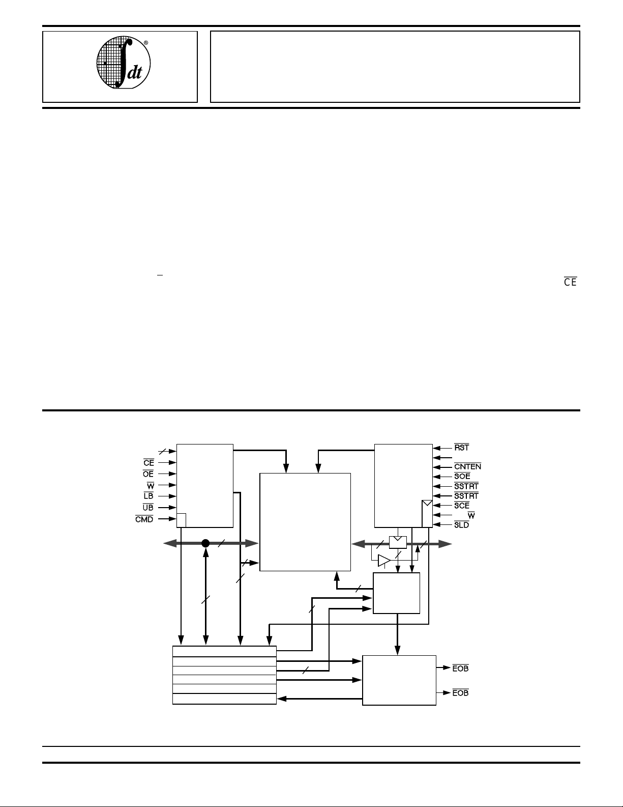
FUNCTIONAL BLOCK DIAGRAM
13
A
0-12
Random
R/
I/O0-15
LSB
MSB
Access
Port
Controls
16
13
Start Address for Buffer #1
End Address for Buffer #1
Start Address for Buffer #2
End Address for Buffer #2
Flow Control Buffer
Flag Status
SCLK
Sequential
Access
Port
Controls
8K X 16
Memory
Array
Data
Addr
R
R
Data
L
13
Addr
L
13
13
13
16
13
COMPARATOR
Reg.
13
Pointer/
Counter
16
RST
1
2
SR/
SI/O0-15
1
2
3016 drw 01
The IDT logo is a registered trademark and SARAM is a trademark of Integrated Device Technology, Inc.
MILITARY AND COMMERCIAL TEMPERATURE RANGES OCTOBER 1996
©1996 Integrated Device Technology, Inc. DSC-3016/6
For latest information contact IDT’s web site at www.idt.com or fax-on-demand at 408-492-8391.
6.31 1
IDT70825S/L
HIGH-SPEED 8K x 16 SEQUENTIAL ACCESS RANDOM ACCESS MEMORY MILITARY AND COMMERCIAL TEMPERATURE RANGES
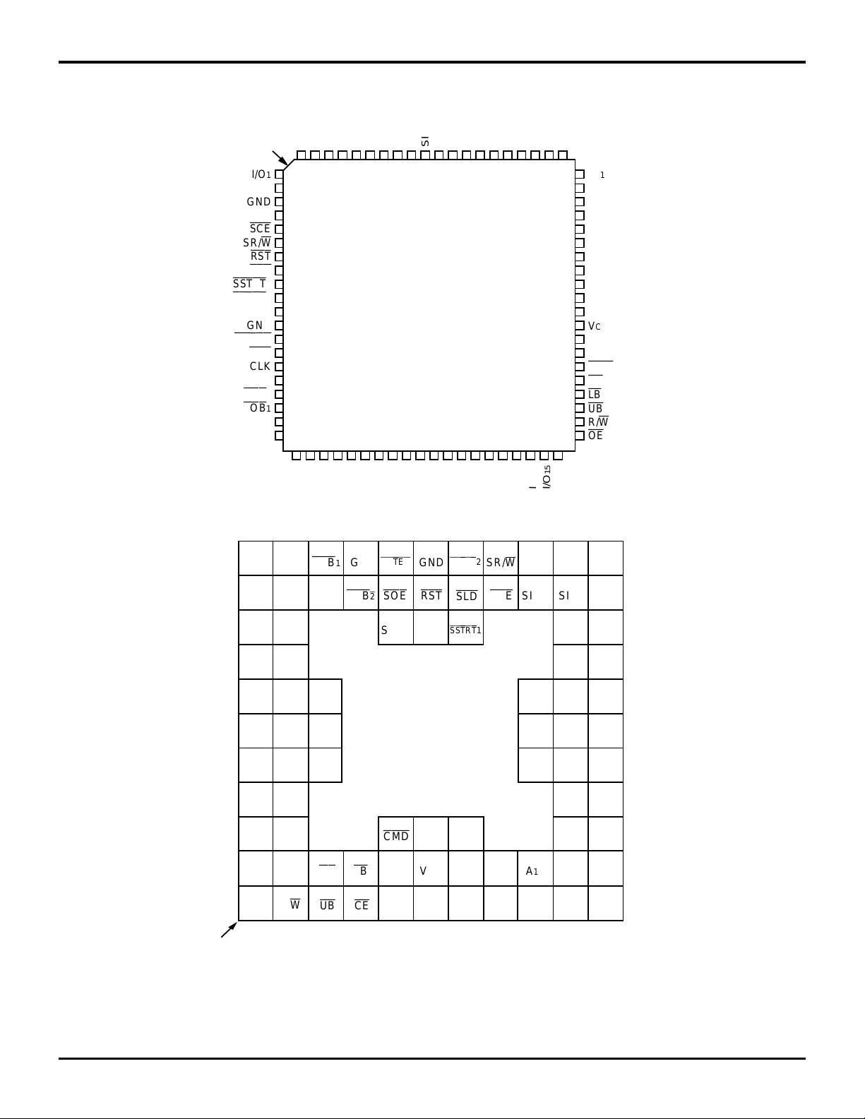
PIN CONFIGURATIONS
(1,2)
INDEX
SI/O
SI/O
GND
N/C
SCE
SR/
RST
SLD
SSTRT
SSTRT
GND
GND
CNTEN
SOE
SCLK
GND
EOB
EOB
V
I/O
2
SI/O
80 79 78 77 76 75 74 73 72 71
1
1
0
2
3
4
5
W
6
7
8
2
9
1
10
11
12
13
14
15
16
2
17
1
18
CC
19
0
20
21 22 36 37 38 39 40
1
I/O
GND
5
3
4
CC
V
SI/O
SI/O
SI/O
23 24 25 26 27 28 29 30 31 32 33 34 35
4
2
3
CC
V
I/O
I/O
I/O
6
SI/O
5
I/O
7
SI/O
6
I/O
GND
8
10
9
SI/O
SI/O
SI/O
70 69 68 67 66 65
IDT70825
PN80-1
TQFP
TOP
(3)
VIEW
7
8
I/O
I/O
GND
11
SI/O
9
I/O
10
I/O
CC
V
11
I/O
12
SI/O
CC
V
13
SI/O
12
I/O
14
SI/O
13
I/O
15
SI/O
6364
14
I/O
GND
N/C
62 61
15
I/O
12
A
60
59
58
57
56
55
54
53
52
51
50
49
48
47
46
45
44
43
42
41
3016 drw 02
GND
11
A
A
10
A
9
A
8
A
7
A
6
A
5
A
4
A
3
A
2
V
CC
V
CC
A
1
A
0
CMD
CE
LB
UB
R/
W
OE
63 61 60 58 55 54
V
CC
646562
NC
GND
68
V
CC
71
EOB1GND
0
I/O
73
66
67
69
72
I/O
I/O
I/O
I/O
1
2
3
4
I/O7I/O6GND SI/O
75
I/O
9
76
I/O
10
79
I/O
12
818283
70
77
80
I/O
I/O
I/O
74
5
I/O
8
78
V
CC
11
13
I/O14NC V
125
OE
GND
I/O
15
8434 6915131618
NC
R/
W
UB
CNTEN
GND
59 56 49
EOB2SOE
RST
57 53
SCLK GND
IDT70825
G84-3
84-PIN PGA
TOP VIEW
7
CMD
811101214 17 20
LB
CE
CC
A
0
CC
V
A
5
1
A
48 46 45
51
SSTRT
50
SLD
52
SSTRT
2
1
NC
SR/W GND NC
47 44
SCE
SI/O
33 35
32 31
SI/O
(3)
28 29
SI/O
2
A
A
7
4
A
A
3
A
A
6
12
10
A
8
ABCDEFGHJKL
INDEX
43
SI/O
0
41
SI/O
38
SI/O4SI/O
8
SI/O
9
SI/O
V
CC
26
SI/O
23
NC SI/O
22 24
A
12
19 21
A9A
10
14
1
2
7
42
40
SI/O
39
V
37
34
GND
36
SI/O
30
SI/O
27
SI/O
25
GND
CC
3
5
6
11
13
15
11
3016 drw 03
11
10
09
08
07
06
05
04
03
02
01
NOTES:
1. All V
CC pins must be connected to power supply.
2. All GND pins must be connected to ground supply.
3. This text does not indicate orientation of the actual part-marking.
6.31 2
IDT70825S/L
HIGH-SPEED 8K x 16 SEQUENTIAL ACCESS RANDOM ACCESS MEMORY MILITARY AND COMMERCIAL TEMPERATURE RANGES
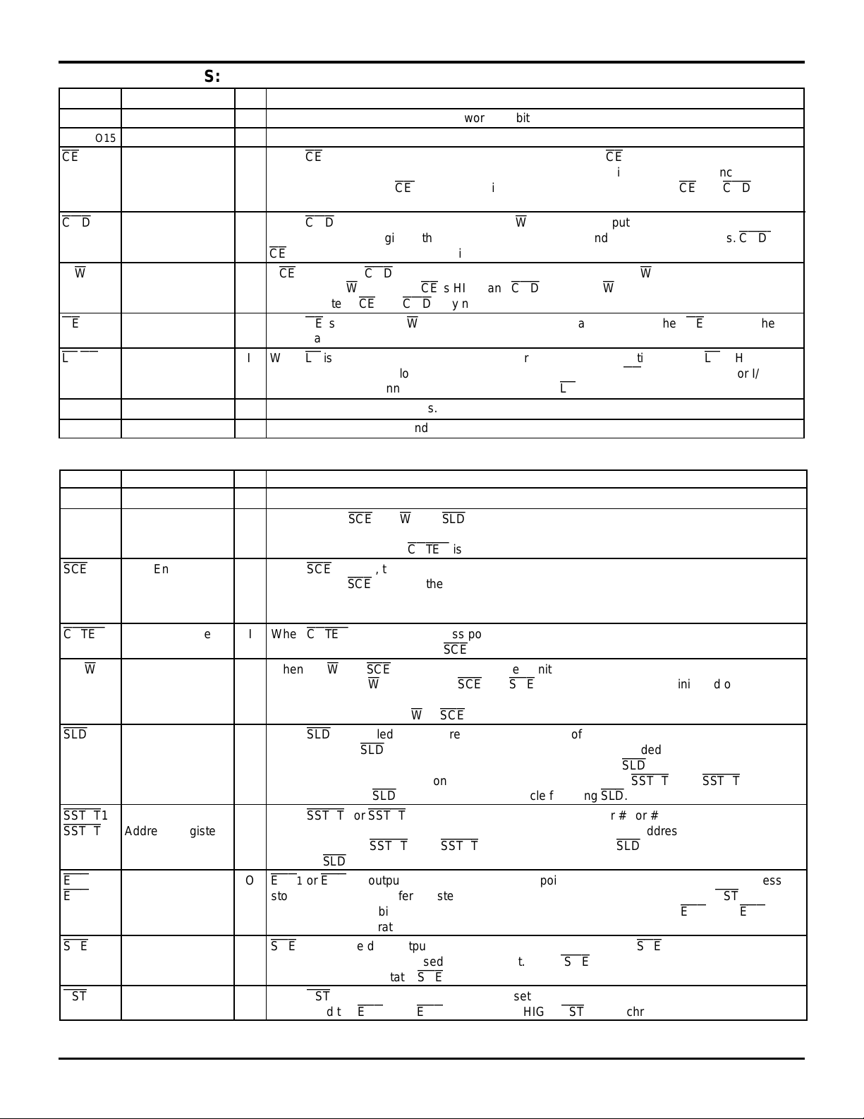
PIN DESCRIPTIONS: RANDOM ACCESS PORT
SYMBOL NAME I/O
A
0-A12 Address Lines I Address inputs to access the 8192-word (16 bit) memory array.
I/
O0-I/O15 Inputs/Outputs I Random access data inputs/outputs for 16-bit wide data.
CE
CMD
Chip Enable I When CE is LOW, the random access port is enabled. When CE is HIGH, the random access
Control Register I When
Enable access the control register, the flag register, and the start and end of buffer registers.
R/
W
OE
LB,UB
Read/Write Enable I If CE is LOW and
Output Enable I When OE is LOW and R/W is HIGH, I/O0-I/O15 outputs are enabled. When OE is HIGH, the I/O
Lower Byte, Upper I When LB is LOW, I/O0-I/O7 are accessible for read and write operations. When LB is HIGH, I/
Byte Enables I/
V
CC Power Supply Seven +5V power supply pins. All Vcc pins must be connected to the same +5V VCC supply.
GND Ground Ten Ground pins. All Ground pins must be connected to the same Ground supply.
(1)
DESCRIPTION
port is disabled into power-down mode and the I/O outputs are in the high-impedance state. All
data is retained during
CE
= VIH, unless it is altered by the sequential port. CE and
CMD
be LOW at the same time.
CMD
is LOW, Address lines A
0-A2, R/
W
, and inputs/outputs I/O0-I/O11, are used to
CMD
CE
may not be LOW at the same time.
CMD
is HIGH, data is written into the array when R/W is LOW and read out of the
array when R/W is HIGH. If CE is HIGH and
mand registers. CE and
CMD
may not be LOW at the same time.
CMD
is LOW, R/W is used to access the buffer com-
outputs are in the high-impedance state.
O7 are tri-stated and blocked during read and write operations.
I/
O15 in the same manner and is asynchronous from
LB
.
UB
controls access for I/O8-
may not
and
O0-
3016 tbl 01
PIN DESCRIPTIONS: SEQUENTIAL ACCESS PORT
SYMBOL NAME I/O
SI/O0-15 Inputs I/O Sequential data inputs/outputs for 16-bit wide data.
SCLK Clock I SI/
SCE
CNTEN
SR/
SLD
Chip Enable I When
Counter Enable I When
W
Read/Write Enable I When SR/W and
Address Pointer I When
Load Control changes. When
SSTRT
1, Load Start of I When
SSTRT
2 Address Register address pointer on the LOW-to-HIGH transition of SCLK. The start addresses are stored in
EOB
1, End of Buffer Flag O
EOB
2 stored in the end of buffer registers. The flags can be cleared by either asserting
SOE
RST
NOTE:
1. "I/O" is bidirectional Input and Output. "I" is Input and "O" is Output.
Output Enable I
Reset I When
(1)
O0-SI/O15,
SCE
, SR/W, and
DESCRIPTION
SLD
are registered on the LOW-to-HIGH transition of SCLK.
Also, the sequential access port address pointer increments by 1 on each LOW-to-HIGH
transition of SCLK when
SCE
is LOW, the sequential access port is enabled on the LOW-to-HIGH transition of
SCLK. When
SCE
CNTEN
is LOW.
is HIGH, the sequential access port is disabled into powered-down mode on
the LOW-to-HIGH transition of SCLK, and the SI/O outputs are in the high-impedance state. All
data is retained, unless altered by the random access port.
CNTEN
is LOW, the address pointer increments on the LOW-to-HIGH transition of SCLK.
This function is independant of
SCE
are LOW, a write cycle is initiated on the LOW-to-HIGH transition of
SCLK. When SR/W is HIGH, and
SCE
.
SCE
and
SOE
are LOW, a read cycle is initiated on the
LOW-to-HIGH transition of SCLK. Termination of a Write cycle is done on the Low-to-High
transistion of SCLK if SR/W or
SLD
is sampled LOW, there is an internal delay of one cycle before the address pointer
SLD
is LOW, data on the inputs SI/
on the LOW-to-HIGH transition of SCLK. On the cycle following
changes to the address location contained in the data-in register.
not be LOW while
SSTRT
internal registers.
following
EOB
1 or
SLD
EOB
SLD
is LOW or during the cycle following
1 or
SSTRT
SSTRT
.
2 is output LOW when the address pointer is incremented to match the address
by writing zero into bit 0 and/or bit 1 of the control register at address 101.
SCE
is High.
O0-SI/O11 is loaded into a data-in register
SLD
, the address pointer
SSTRT
1 and
SSTRT
2 may
SLD
.
2 is LOW, the start of address register #1 or #2 is loaded into the
1 and
SSTRT
2 may not be LOW while
SLD
is LOW or during the cycle
RST
EOB
1 and
LOW or
EOB
dependent on separate internal registers, and therefore separate match addresses.
SOE
controls the data outputs and is independent of SCLK. When
and the sequentially addressed data is output. When
the high-impedance state.
RST
is LOW, all internal registers are set to their default state, the address pointer is set
to zero and the
EOB
1 and
SOE
is asynchronous to SCLK.
EOB
2 flags are set HIGH.
SOE
RST
is HIGH, the SI/O output bus is in
is asynchronous to SCLK.
SOE
is LOW, output buffers
2 are
3016 tbl 02
6.31 3
IDT70825S/L
HIGH-SPEED 8K x 16 SEQUENTIAL ACCESS RANDOM ACCESS MEMORY MILITARY AND COMMERCIAL TEMPERATURE RANGES
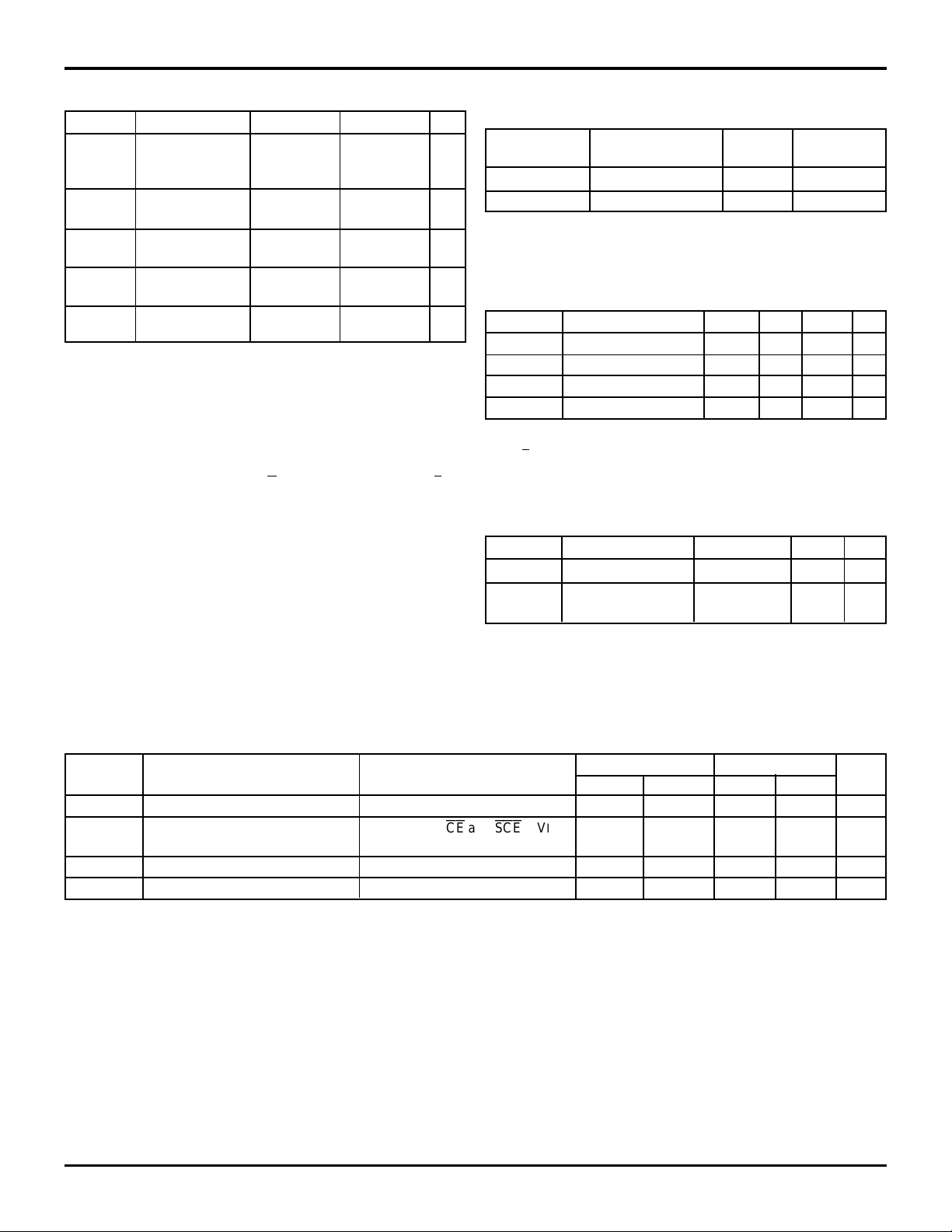
ABSOLUTE MAXIMUM RATINGS
(1)
Symbol Rating Commercial Military Unit
(2)
V
TERM
Terminal Voltage –0.5 to +7.0 –0.5 to +7.0 V
with Respect
to GND
T
A Operating 0 to +70 –55 to +125 ° C
Temperature
T
BIAS Temperature –55 to +125 –65 to +135 °C
Under Bias
T
STG Storage –55 to +125 –65 to +150 °C
Temperature
I
OUT DC Output 50 50 mA
Current
NOTES: 3016 tbl 03
1. Stresses greater than those listed under ABSOLUTE MAXIMUM RATINGS may cause permanent damage to the device. This is a stress rating
only and functional operation of the device at these or any other conditions
above those indicated in the operational sections of this specification is not
implied. Exposure to absolute maximum rating conditions for extended
periods may affect reliability.
TERM must not exceed Vcc + 0.5V for more than 25% of the cycle time
2. V
or 10ns maximum, and is limited to
+ 0.5V.
< 20mA for the period of VTERM > Vcc
RECOMMENDED OPERATING
TEMPERATURE AND SUPPLY VOLTAGE
Ambient
Grade Temperature GND VCC
Military –55°C to +125°C 0V 5.0V ± 10%
Commercial 0°C to +70°C 0V 5.0V ± 10%
3016 tbl 04
RECOMMENDED DC OPERATING
CONDITIONS
Symbol Parameter Min. Typ. Max. Unit
V
CC Supply Voltage 4.5 5.0 5.5 V
GND Supply Voltage 0 0 0 V
V
IH Input High Voltage 2.2 — 6.0
V
IL Input Low Voltage –0.5
NOTES: 3016 tbl 05
1. VIL > –1.5V for pulse width less than 10ns.
TERM must not exceed Vcc + 0.5V.
2. V
CAPACITANCE
(1)
(1)
— 0.8 V
(TA = +25°C, F = 1.0MHz)TQFP ONLY
Symbol Parameter Conditions
C
IN Input Capacitance VIN = 3dV 9 pF
C
OUT Output VOUT = 3dV 10 pF
Capacitance
NOTES: 3016 tbl 06
1. This parameter is determined by device characterization, but is not
production tested.
2. 3dV references the interpolated capacitance when the input and output
signals switch from 0V to 3V or from 3V to 0V.
(2)
(2)
V
Max. Unit
DC ELECTRICAL CHARACTERISTICS OVER THE OPERATING TEMPERATURE
AND SUPPLY VOLTAGE RANGE (V
Symbol Parameter Test Conditions Min. Max. Min. Max. Unit
LI| Input Leakage Current
|I
|I
LO| Output Leakage Current VCC = Max.
VOL Output Low Voltage IOL = 4mA, VCC = Min. — 0.4 — 0.4 V
V
OH Output High Voltage IOH = –4mA, VCC = Min. 2.4 — 2.4 — V
NOTE:
1. At Vcc ≤ 2.0V input leakages are undefined.
(1)
CC = 5.0V ± 10%)
IDT70825S IDT70825L
VCC = Max. VIN = GND to VCC — 5.0 — 1.0 µA
CE
and
SCE
= VIH — 5.0 — 1.0 µA
V
OUT = GND to VCC
3016 tbl 07
6.31 4
IDT70825S/L
HIGH-SPEED 8K x 16 SEQUENTIAL ACCESS RANDOM ACCESS MEMORY MILITARY AND COMMERCIAL TEMPERATURE RANGES
DC ELECTRICAL CHARACTERISTICS OVER THE OPERATING TEMPERATURE
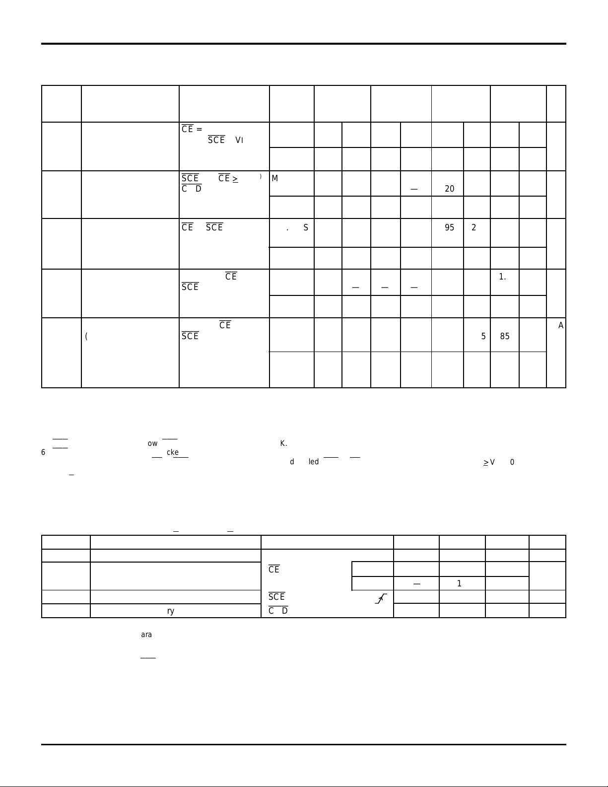
(1)
AND SUPPLY VOLTAGE RANGE
Symbol Parameter Condition Version Typ.
I
CC Dynamic Operating
Current Open,
(Both Ports Active) f = f
SB1 Standby Current
I
(Both Ports - TTL Level
Inputs) f = f
I
SB2 Standby Current
(One Port - TTL Level Active Port Outputs L —— — — 95 250 90 250
Input) Open, f = f
I
SB3 Full Standby Current Both Ports
(Both Ports - CMOS
Level Inputs) V
I
SB4 Full Standby Current One Port
(One Port - CMOS
Level Inputs) Outputs Open
NOTES:
1. "X" in part number indicates power rating (S or L).
2. V
CC = 5V, Ta = +25°C; guaranteed by device characterization but not production tested.
3. At f = f
4. f = 0 means no address or control lines change.
5.
6.
7. If one port is enabled (either CE or
MAX, address, control lines (except Output Enable), and SCLK are cycling at the maximum frequency read cycle of 1/tRC.
SCE
may transition, but is Low (
SCE
may be ≤ 0.2V, after it is clocked in, since SCLK=V
< 0.2V, and TTL High = VIH and Low = VIL.
Low
CE
= VIL, Outputs MIL. S — — — — 160 400 155 400 mA
MAX
SCE
and CE > VIH
CMD
= V
MAX
CE
or
SCE
≥ V
IN ≥ VCC - 0.2V or COM’L.S 1.0 15 1.0 15 1.0 15 1.0 15
V
IN ≤ 0.2V, f = 0
SCE
≥ V
(Active port), f
V
IN ≥ VCC - 0.2V or
V
IN ≤ 0.2V L 110 200 100 190 90 180 85 180
IL) when clocked in by SCLK.
SCE
=V
SCE
= Low) then the other port is disabled (
(VCC = 5.0V ± 10%)
70825X20 70825X25 70825X35 70825X45
Test Com'l. Only Com'l. Only
SCE
(3)
= V
IL
COM’L. S 180 380 170 360 160 340 155 340
L — — — — 160 340 155 340
(5)
L 180 330 170 310 160 290 155 290
(7)
MIL. S — — — — 20 85 16 85 mA
IH L— — — — 20 6516 65
(3)
COM’L. S 25 70 25 70 20 70 16 70
L25502550 20501650
SCE
= VIH MIL. S — — — — 95 290 90 290 mA
(3)
MAX
COM’L. S 115 260 105 250 95 240 90 240
L 115 230 105 220 95 210 90 210
CE
and MIL. S — — — — 1.0 30 1.0 30 mA
CC - 0.2V
CE
CC - 0.2V
(6,7)
(4)
L — — — — 0.2 10 0.2 10
L 0.2 5 0.2 5 0.2 5 0.2 5
or MIL. S — — — — 90 260 85 260 mA
(6)
(3)
= fMAX
COM’L. S 110 240 100 230 90 220 85 220
IH must be clocked in prior to powerdown.
L — — — — 90 215 85 215
(2)
Max. Typ.
SCE
or CE = High, respectively). CMOS High
(2)
Max. Typ.
(2)
Max. Typ.
(2)
> Vcc - 0.2V and
Max. Unit
3016 tbl 08
DATA RETENTION CHARACTERISTICS OVER ALL TEMPERATURE RANGES
(L VERSION ONLY)
Symbol Parameter Test Condition Min. Typ.
V
DR VCC for Data Retention VCC = 2V 2.0 — — V
I
CCDR Data Retention Current
(3)
t
CDR
(3)
t
R
NOTES :
1. T
A = +25°C, VCC = 2V; guaranteed by device characterization but not production tested.
RC = Read Cycle Time
2. t
3. This parameter is guaranteed by device characterization, but is not production tested.
4. To initiate data retention,
Chip Deselect to Data Retention Time
Operation Recovery Time
(VLC < 0.2V, VHC > VCC - 0.2V)
IH must be clocked in.
SCE
= V
(1)
Max. Unit
CE
= VHC MIL. — 100 4000 µA
V
IN = VHC or = VLC COM’L. — 100 1500
SCE
CMD
(4)
= VHC
= VHC tRC
when SCLK= 0 — — ns
(2)
6.31 5
——ns
3016 tbl 09
IDT70825S/L
1
2
3
4
5
6
7
8
20 40 60 80 100 120 140 160 180
200
CAPACITANCE (pF)
10pF is the I/O
capacitance of
this device, and
30pF is the AC
Test Load
capacitance.
3016 drw 07
tAA/tCD/tEB
(Typical, ns)
-1
-2
-3
HIGH-SPEED 8K x 16 SEQUENTIAL ACCESS RANDOM ACCESS MEMORY MILITARY AND COMMERCIAL TEMPERATURE RANGES
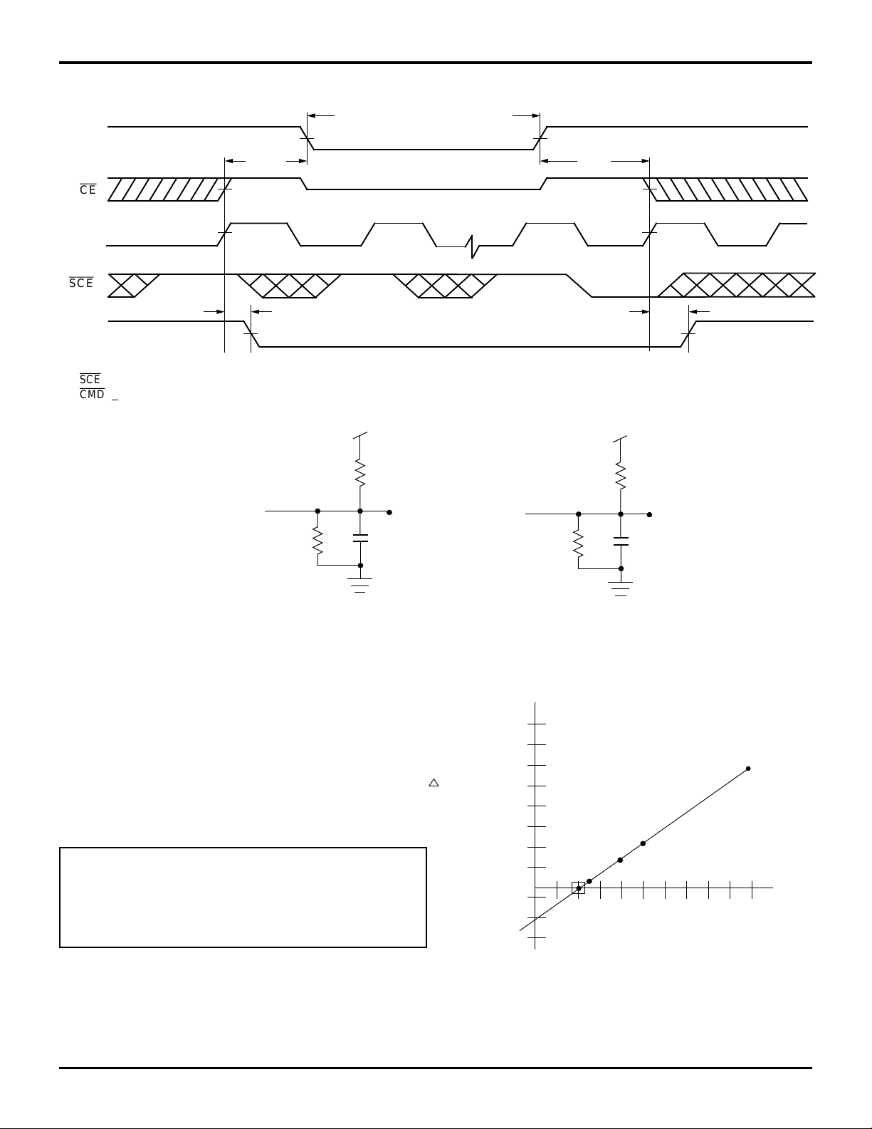
DATA RETENTION AND POWER DOWN/UP WAVEFORM (RANDOM AND SEQUENTIAL PORT)
(1,2)
DATA RETENTION MODE
V
CC
CE
4.5V
t
CDR
V
IH
≥
V
DR
2V
V
DR
4.5V
t
R
V
IH
SCLK
SCE
t
I
CC
NOTES :
1.
SCE
is synchronized to the sequential clock input.
CMD
> VCC - 0.2V.
2.
PD
I
SB
t
PU
I
SB
3016 drw 04
AC TEST CONDITIONS
Input Pulse Levels GND to 3.0V
Input Rise/Fall Times 3ns Max.
Input Timing Reference Levels 1.5V
Output Reference Levels 1.5V
AC Test Load Figures 1, 2, and 3
DATA
OUT
Figure 1. AC Output Test Load
5V
893Ω
30pF347Ω
3016 drw 05
5V
893Ω
DATA
OUT
5pF347Ω
3016 drw 06
Figure 2. Output Test Load (for tCLZ, tBLZ, tOLZ, tCHZ,
3016 tbl 10
Figure 3. Lumped Capacitance Load Typical Derating Curve
6.31 6
t
BHZ, tOHZ, tWHZ, tCKHZ, and tCKLZ)
Including scope and jig.
IDT70825S/L
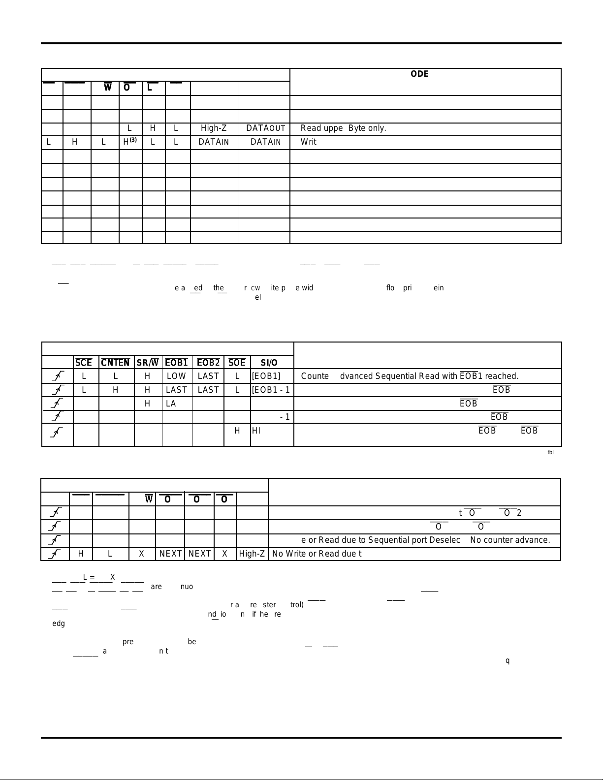
HIGH-SPEED 8K x 16 SEQUENTIAL ACCESS RANDOM ACCESS MEMORY MILITARY AND COMMERCIAL TEMPERATURE RANGES
TRUTH TABLE I – RANDOM ACCESS READ AND WRITE
(1,2)
Inputs/Outputs MODE
CECE
CE
CECE
CMDCMD
CMD
CMDCMD
R/
WW
OEOE
LBLB
W
OE
WW
OEOE
LB
LBLB
UBUB
UB
UBUB
I/O
0-I/O7 I/O8-I/O-
L H H L L L DATAOUT DATAOUT Read both Bytes.
L H H L L H DATA
L H H L H L High-Z DATA
LH LH
LH LH
LH LH
(3)
L L DATAIN DATAIN Write to both Bytes.
(3)
L H DATAIN High-Z Write to lower Byte only.
(3)
H L High-Z DATAIN Write to upper Byte only.
OUT High-Z Read lower Byte only.
OUT Read upper Byte only.
H H X X X X High-Z High-Z Both Bytes deselected and powered down.
L H H H X X High-Z High-Z Outputs disabled but not powered down.
L H X X H H High-Z High-Z Both Bytes deselected but not powered down.
HL LH
HL HLL
NOTES:
1. H = V
2.
3. If OE = V
4. Byte operations to control register using UB and LB separately are also allowed.
IH, L = VIL, X = Don't Care, and High-Z = High-impedance.
RST, SCE, CNTEN
operation.
IL during write, tWHZ must be added to the tWP or tCW write pulse width to allow the bus to float prior to being driven.
TRUTH TABLE II – SEQUENTIAL READ
(3)L(4)L(4)
, SR/W,
SLD, SSTRT
(4)L(4)
DATAIN DATAIN Write I/O0-I/O12 to the Buffer Command Register.
DATAOUT DATAOUT Read contents of the Buffer Command Register via I/O0-I/O12.
1,
SSTRT
2, SCLK, SI/O
(1,2,3,6,8)
0-SI/O15,
EOB
1,
EOB
2, and
SOE
are unrelated to the random access port control and
Inputs/Outputs MODE
SCLK
SCE
SCESCE
CNTENCNTEN
CNTEN
CNTENCNTEN
SR/
W
WW
WW
EOB1EOB1
EOB1
EOB1EOB1
EOB2EOB2
EOB2
EOB2EOB2
SOESOE
SOE
SOESOE
SI/O
SCESCE
L L H LOW LAST L [EOB1] Counter Advanced Sequential Read with
L H H LAST LAST L [EOB1 - 1] Non-Counter Advanced Sequential Read, without
L L H LAST LOW L [EOB2] Counter Advanced Sequential Read with
L H H LAST LAST L [EOB2 - 1] Non-Counter Advanced Sequential Read without
L L H LOW LOW H HIGH-Z Counter Advanced Sequential Non-Read with
reached.
TRUTH TABLE III – SEQUENTIAL WRITE
(1,2,3,4,5,6,7,8)
Inputs/Outputs MODE
SCESCE
SCLK
CNTENCNTEN
SCE
CNTEN
SCESCE
CNTENCNTEN
L H L LAST LAST H SI/O
L L L LOW LOW H SI/O
SR/
WW
W
WW
EOB1EOB1
EOB1
EOB1EOB1
EOB2EOB2
EOB2
EOB2EOB2
SOESOE
SOE
SOESOE
SI/O
IN Non-Counter Advanced Sequential Write, without
IN Counter Advanced Sequential Write with
EOB
1 and
H H X LAST LAST X High-Z No Write or Read due to Sequential port Deselect. No counter advance.
H L X NEXT NEXT X High-Z No Write or Read due to Sequential port Deselect. Conter does advance.
NOTES:
1. H = V
2.
3.CE, OE, R/W,
4.
5. SI/
6. "LAST" refers to the previous value still being output, no change.
7. Termination of a write is done on the Low-to-High transition of SCLK if SR/W or
8. When
IH, L = VIL, X = Don't Care, and High-Z = High-impedance. LOW = VOL.
RST, SLD, SSTRT
with the sequential port operation (due to the counter and register control).
SOE
must be HIGH (
edge of the clock during the cycle in which SR/W = V
OIN refers to SI/O0-SI/O15 inputs.
CLKEN
Enable Cycle after Reset, Read (and write) Cycle".
1,
SSTRT
2 are continuously HIGH during a sequential write access, other than pointer access operations.
CMD, LB, UB
SOE
=V
=Low, the address is incremented on the next rising edge before any operation takes place. See the diagrams called "Sequential Counter
0-I/O15 are unrelated to the sequential port control and operation except for
, and I/O
IH) prior to write conditions only if the previous cycle is a read cycle, since the data being written must be an input at the rising
IL.
CMD
should be HIGH (
SCE
is High.
CMD
CMD
which must not be used concurrently
IH) during sequential port access.
= V
EOB
EOB
EOB
EOB
1 reached.
EOB
2 reached.
EOB
2 reached.
EOB
1 and
1 or
EOB
2 reached.
3016 tbl 11
1 reached.
EOB
2
3016 tbl 12
2 reached
3016 tbl 13
6.31 7

IDT70825S/L
HIGH-SPEED 8K x 16 SEQUENTIAL ACCESS RANDOM ACCESS MEMORY MILITARY AND COMMERCIAL TEMPERATURE RANGES
TRUTH TABLE IV – SEQUENTIAL ADDRESS POINTER OPERATIONS
(1,2,3,4,5)
Inputs/Outputs
SCLK
SLD
SLDSLD
SSTRTSSTRT
SSTRT
SSTRTSSTRT
1
SSTRTSSTRT
SSTRT
SSTRTSSTRT
SOESOE
SOE
2
SOESOE
MODE
SLDSLD
H L H X Start address for Buffer #1 loaded into Address Pointer.
H H L X Start address for Buffer #2 loaded into Address Pointer.
LH HH
NOTES: 3016 tbl 14
1. H = VIH, L = VIL, X = Don't Care, and High-Z = High-impedance.
2.
RST
is continuously HIGH. The conditions of
3.CE, OE, R/W, LB, UB, and I/O
the sequential port operation (due to the counter and register control).
4. Address pointer can also change when it reaches an end of buffer address. See Flow Control Bits table.
5. When
6.
SLD
is not incremented during the two cycles.
SOE
is sampled LOW, there is an internal delay of one cycle before the address pointer changes. The state of
may be LOW with
0-I/O15 are unrelated to the sequential port control and operation, except for
SCE
deselect or in the write mode using SR/W.
(6)
Data on SI/O0-SI/O12 loaded into Address Pointer.
SCE, CNTEN
, and SR/W are unrelated to the sequential address pointer operations.
CMD
should be HIGH (CMD = V
CMD
which must not be used concurrently with
IH) during sequential port access.
CNTEN
is ignored and the address
ADDRESS POINTER LOAD CONTROL (SLD)
In
SLD
mode, there is an internal delay of one cycle before
the address pointer changes in the cycle following
SLD
is LOW, data on the inputs SI/O0-SI/O12 is loaded into a
SLD
data-in register on the LOW-to-HIGH transition of
the cycle following
SLD
, the address pointer changes to the
. When
SCLK
. On
address location contained in the data-in register.
SSTRT
2 may not be low while
following
SLD
. The
SSTRT
SLD
is LOW, or during the cycle
1 and
SSTRT
2 require only one
clock cycle, since these addresses are pre-loaded in the
registers already.
SSTRT
1,
SLDSLD
SLD
SLDSLD
MODE
(1)
SLD
(1)
SCLK
A
ADDR
0-11
SI/O
SSTRT
1,2
NOTE:
1. At SCLK edge (A), SI/O
address pointer changes). At SCLK edge (A),
(B),
SLD
and
for edge (B), while data will not be ready at edge (B) when
SSTRT
0-SI/O12 data is loaded into a data-in register. At edge (B), contents of the data-in register are loaded into the address pointer (i.e.
SSTRT
1,2 must be high to ensure for proper sequential address pointer loading. For
1 and
SSTRT
SLD
IN
2 must be high to ensure for proper sequential address pointer loading. At SCLK edge
is used, but will be ready at edge (C).
SEQUENTIAL LOAD OF ADDRESS INTO POINTER/COUNTER
B
(1)
SSTRT
1 or
C
DATA
OUT
SSTRT
2, the data to be read will be ready
3016 drw 08
MSB
NOTE:
1. "H" = V
15
14 13
H
HHH
IH for the SI/O intput state.
12 ------------------------------------------------------------------------------------------------------------
Address Loaded into Pointer
6.31 8
0
LSB SI/O BITS
3016 drw 09

IDT70825S/L
HIGH-SPEED 8K x 16 SEQUENTIAL ACCESS RANDOM ACCESS MEMORY MILITARY AND COMMERCIAL TEMPERATURE RANGES
Reset (
RST
RSTRST
RST
)
RSTRST
Setting
RST
LOW resets the control state of the SARAM.
functions asynchronously of SCLK, (i.e. not registered).
The default states after a reset operation are as follows:
Register Contents
Address Pointer 0
EOB Flags Cleared to High state
Buffer Flow Mode BUFFER CHAINING
Start Address Buffer #1 0 (1)
End Address Buffer #1 4095 (4K)
Start Address Buffer #2 4096 (4K+1)
End Address Buffer #2 8191 (8K)
Registered State
BUFFER COMMAND MODE (
Buffer Command Mode (
port to control the state of the two buffers. Address pins A0-A2
and I/O pins I/O0-I/O12 are used to access the start of buffer
and the end of buffer addresses and to set the flow control
SCE
= V
IH, SR/
CMDCMD
CMD
)
CMDCMD
CMD
) allows the random access
W
= VIL
3016 tbl 15
reading and clearing the status of the EOB flags. Seven
different CMD cases are available depending on the conditions of A0-A2 and R/W. Address bits A3-A12 and data I/O bits
I/O13-I/O15 are not used during this operation.
mode of each buffer. The Buffer Command Mode also allows
RANDOM ACCESS PORT
Case # A2-A0 R/
1 000 0 (1) Write (read) the start address of Buffer #1 through I/O
2 001 0 (1) Write (read) the end address of Buffer #1 through I/O
3 010 0 (1) Write (read) the start address of Buffer #2 through I/O
4 011 0 (1) Write (read) the end address of Buffer #2 through I/O
5 100 0 (1) Write (read) flow control register
6 101 0 Write only – clear EOB
7 101 1 Read only – flag status register
8 110/111 (X) (Reserved)
NOTE:
1. R/W input "0(1)" indicates a write(0) or read(1) occurring with the same address input.
CMDCMD
CMD
CMDCMD
MODE
WW
W
WW
(1)
1 and/or EOB2 flag
DESCRIPTIONS
0-I/O12.
0-I/O12.
0-I/O12.
0-I/O12.
3016 tbl 16
CASES 1 THROUGH 4: START AND END OF BUFFER REGISTER DESCRIPTION
15
14 13
MSB LSB I/O BITS
NOTES:
1. "H" = V
2. A write into the buffer occurs when R/W = V
H
OH for I/O in the output state and "Don't Cares" for I/O in the input state.
IL and
CE
= V
= VIH.
12 ------------------------------------------------------------------------------------------------------------
HH
IL and a read when R/
Address Loaded into Buffer
W
= VIH.
EOB1/SOB
1 and
EOB2/SOB
2 are chosen through address A0-A2 while
(1,2)
0
3016 drw 10
CMD
CASE 5: BUFFER FLOW MODES
Within the SARAM, the user can designate one of four
buffer flow modes for each buffer. Each buffer flow mode
defines a unique set of actions for the sequential port address
pointer and EOB flags. In BUFFER CHAINING mode, after the
address pointer reaches the end of the buffer, it sets the
corresponding EOB flag and continues from the start address
of the other buffer. In STOP mode, the address pointer stops
incrementing after it reaches the end of the buffer. In LINEAR
mode, the address pointer ignores the end of buffer address
and increments past it, but sets the EOB flag. MASK mode is
the same as LINEAR mode except EOB flags are not set.
6.31 9

IDT70825S/L
HIGH-SPEED 8K x 16 SEQUENTIAL ACCESS RANDOM ACCESS MEMORY MILITARY AND COMMERCIAL TEMPERATURE RANGES
FLOW CONTROL REGISTER DESCRIPTION
15
MSB
HHH HHH432 1 0HHHH
H
(1,2)
0
LSB I/O BITS
Counter Release
(STOP Mode Only)
NOTES:
1. "H" = V
2. Writing a 0 into bit 4 releases the address pointer after it is stopped due to the STOP mode and allows sequential write operations to resume. This occurs
OH for I/O in the output state and "Don't Cares"' for I/O in the input state.
asynchronously of SCLK, and therefore caution should be taken. The pointer will be at address EOB+2 on the next rising edge of SCLK that is enabled
by
CNTEN
. The pointer is also released by
RST, SLD, SSTRT
1 and
SSTRT
2 operations.
Buffer #2 flow control
Buffer #1 flow control
3016 drw 11
FLOW CONTROL BITS
Flow Control Bits
Bit 1 & Bit 0 Mode
(Bit 3 & Bit 2) Functional Description
00 BUFFER
CHAINING #1 (Buffer #2). The pointer value is changed to the start address of Buffer #2 (Buffer #1).
01 STOP
10 LINEAR
11 MASK
NOTES:
1.
EOB
1 and
EOB
2.
CMD
Flow Control bits are unchanged, the count does not continue advancement.
3. If
EOB
4. If counter has stopped at EOBx and was released by bit 4 of the flow control register,
the flow control will remain in the STOP mode.
2 may be asserted (set) at the same time, if both end addresses have been loaded with the same value.
1 and
EOB
2 are equal, then the pointer will jump to the start of Buffer #1.
EOB
1 (
EOB
2) is asserted (Active Low output) when the pointer matches the end address of Buffer
EOB
1 (
EOB
2) is asserted when the pointer matches the end address of Buffer #1 (Buffer #2).
The address pointer will stop incrementing when it reaches the next address (
CNTEN
EOB
released by bit 4 of the flow control register.
EOB
The pointer keeps incrementing for further operations.
EOB
is Low on the next clock's rising edge. Otherwise, the address pointer will stop incrementing on
. Sequential write operations are inhibited after the address pointer is stopped. The pointer can be
1 (
EOB
2) is asserted when the pointer matches the end address of Buffer #1 (Buffer #2).
1 (
EOB
2) is not asserted when the pointer reaches the end address of Buffer #1 (Buffer #2),
(1,2,4)
(1)
EOB
(1,3)
address + 1), if
although the flag status bits will be set. The pointer keeps incrementing for further operations.
CNTEN
must be LOW on the next rising edge of SCLK otherwise
3016 tbl 17
CASES 6 AND 7: FLAG STATUS REGISTER BIT DESCRIPTION
15
MSBHHH HHH HH HH HH H 1 0
NOTE:
1. "H" = V
OH for I/O in the output state and "Don't Cares" for I/O in the input state.
CASE 6: FLAG STATUS REGISTER WRITE CONDITIONS
H
(1)
(1)
0
End of buffer flag for Buffer #1
End of buffer flag for Buffer #2
Flag Status Bit 0, (Bit 1) Functional Description
0 Clears Buffer Flag
1 No change to the Buffer Flag.
NOTES: 3016 tbl 18
1. Either bit 0 or bit 1, or both bits, may be changed simultaneously. One may be cleared while the second is left alone or cleared.
2. Remains as it was prior to the
CMD
operation, either HIGH (1) or LOW (0).
EOB
1, (
EOB
2).
(2)
CASE 7: FLAG STATUS REGISTER READ CONDITIONS
Flag Status Bit 0, (Bit 1) Functional Description
0
1
EOB
1 (
EOB
2) flag has not been set, the
Pointer has not reached the End of the
Buffer.
EOB
1 (
EOB
2) flag has been set, the
Pointer has reached the End of the Buffer.
3016 tbl 19
LSB I/O BITS
3016 drw 12
6.31 10

IDT70825S/L
HIGH-SPEED 8K x 16 SEQUENTIAL ACCESS RANDOM ACCESS MEMORY MILITARY AND COMMERCIAL TEMPERATURE RANGES
CASES 8 AND 9: (RESERVED)
Illegal operations. All outputs will be HIGH on the I/O bus during a READ.
RANDOM ACCESS PORT: AC ELECTRICAL CHARACTERISTICS OVER THE
OPERATING TEMPERATURE AND SUPPLY VOLTAGE RANGE
IDT70825X20 IDT70825X25 IDT70825X35 IDT70825X45
Com'l. Only Com'l. Only
Symbol Parameter Min. Max. Min. Max. Min. Max. Min. Max. Unit
READ CYCLE
t
RC Read Cycle Time 20 — 25 — 35 — 45 — ns
t
AA Address Access Time — 20 — 25 — 35 — 45 ns
t
ACE Chip Enable Access Time — 20 — 25 — 35 — 45 ns
t
BE Byte Enable Access Time — 20 — 25 — 35 — 45 ns
t
OE Output Enable Access Time — 10 — 10 — 15 — 20 ns
t
OH Output Hold from Address Change 3 — 3 — 3 — 3 — ns
t
CLZ Chip Select Low-Z Time
t
BLZ Byte Enable Low-Z Time
t
OLZ Output Enable Low-Z Time
t
CHZ Chip Select High-Z Time
t
BHZ Byte Enable High-Z Time
t
OHZ Output Enable High-Z Time
t
PU Chip Select Power-Up Time 0 — 0 — 0 — 0 — ns
t
PD Chip Select Power-Down Time — 20 — 25 — 35 — 45 ns
NOTES:
1. Transition measured at ±200mV from steady state. This parameter is guaranteed with the AC Test Load (Figure 2) by device characterization, but is not
production tested.
2. "X" in part number indicates power rating (S or L).
3.
CMD
access follows standard timing listed for both read and write accesses, ( CE = V
(1)
(1)
(1)
(1)
(1)
(1)
3 —3—3—3—ns
3 —3—3—3—ns
2 —2—2—2—ns
— 10 — 12 — 15 — 15 ns
— 10 — 12 — 15 — 15 ns
— 9—11—15—15ns
IH when
(2,3)
CMD
= VIL ) or (
CMD
= VIH when CE = VIL ).
3016 tbl 20
RANDOM ACCESS PORT: AC ELECTRICAL CHARACTERISTICS
OVER THE OPERATING TEMPERATURE AND SUPPLY VOLTAGE
IDT70825X20 IDT70825X25 IDT70825X35 IDT70825X45
Com'l. Only Com'l. Only
Symbol Parameter Min. Max. Min. Max. Min. Max. Min. Max. Unit
WRITE CYCLE
t
WC Write Cycle Time 20 — 25 — 35 — 45 — ns
t
CW Chip Select to End-of-Write 15 — 20 — 25 — 30 — ns
t
AW Address Valid to End-of-Write
t
AS Address Set-up Time 0 — 0 — 0 — 0 — ns
t
WP Write Pulse Width
t
BP Byte Enable Pulse Width
t
WR Write Recovery Time 0 — 0 — 0 — 0 — ns
t
WHZ Write Enable Output High-Z Time
t
DW Data Set-up Time 13 — 15 — 20 — 25 — ns
t
DH Data Hold Time 0 — 0 — 0 — 0 — ns
t
OW Output Active from End-of-Write 3 — 3 — 3 — 3 — ns
NOTES:
1. Transition measured at ±200mV from steady state. This parameter is guaranteed with the AC Test Load (Figure 2) by device characterization, but is not
production tested.
2. "X" in part number indicates power rating (S or L).
3.OE is continuously HIGH, OE = V
drivers to turn off and on the data to be placed on the bus for the required t
not apply and the minimum write pulse is the specified t
4.
CMD
access follows standard timing listed for both read and write accesses, ( CE = V
(3)
IH. If during the R/
(3)
15 — 20 — 25 — 30 — ns
13 — 20 — 25 — 30 — ns
(3)
(1)
W
controlled write cycle the OE is LOW, tWP must be greater or equal to tWHZ + tDW to allow the I/O
15 — 20 — 25 — 30 — ns
—10—12 —15—15ns
DW. If
OE
WP. For the
CE
controlled write cycle, OE may be LOW with no degradation to tCW timing.
is HIGH during the R/W controlled write cycle, this requirement does
IH when
CMD
(2,4)
= VIL ) or (
CMD
= VIH when CE = VIL ).
3016 tbl 21
6.31 11

IDT70825S/L
HIGH-SPEED 8K x 16 SEQUENTIAL ACCESS RANDOM ACCESS MEMORY MILITARY AND COMMERCIAL TEMPERATURE RANGES
RANDOM ACCESS PORT WAVEFORM: READ CYCLES
t
RC
ADDR
t
AA
(2)
t
ACS
t
CLZ
,
t
BE
t
BLZ
t
OE
t
OLZ
I/O
OUT
Valid Data Out
(1,2)
t
OH
t
CHZ
t
BHZ
t
OHZ
3016 drw 13
NOTES:
1. R/W is HIGH for Read cycle.
2. Address valid prior to or coincident with CE transition LOW; otherwise t
AA is the limiting parameter.
RANDOM ACCESS PORT WAVEFORM: READ CYCLES BUFFER COMMAND MODE
t
RC
ADDR
t
I/O
,
OUT
(1)
t
CLZ
t
BLZ
AA
t
t
OLZ
ACS
t
BE
t
OE
Valid Data Out
t
OH
t
CHZ
t
BHZ
t
OHZ
3016 drw 14
NOTE:
1. CE = VIH when
CMD
= VIL.
6.31 12

IDT70825S/L
HIGH-SPEED 8K x 16 SEQUENTIAL ACCESS RANDOM ACCESS MEMORY MILITARY AND COMMERCIAL TEMPERATURE RANGES
RANDOM ACCESS PORT WAVEFORM: WRITE CYCLE NO.1 (R/
t
WC
ADDR
t
AW
R/
W
(2)
t
WP
t
DW
Valid Data In
CE, LB, UB
I/O
t
(8)
IN
AS
(5)
OE
t
WHZ
I/O
OUT
Data Out
(4)
t
ACS
t
BE
RANDOM ACCESS PORT WAVEFORM: WRITE CYCLE NO.2
CECE
(
CE
CECE
LBLB
,
LB
, AND/OR
LBLB
UBUB
UB
CONTROLLED TIMING)
UBUB
(1,6,7)
WW
W
CONTROLLED TIMING)
WW
t
WR
t
DH
t
OHZ
Data Out
t
OW
(1,6)
(3)
(4)
3016 drw 15
t
WC
ADDR
t
CE, LB, UB
(8)
t
AS
R/
W
I/O
IN
NOTES:
1. R/W, CE, or LB and UB must be inactive during all address transitions.
2. A write occurs during the overlap of R/W = V
3. t
WR is measured from the earlier of
4. During this period, I/O pins are in the output state and the input signals must not be applied.
5. If the CE LOW transition occurs simultaneously with or after the R/W LOW transition, the outputs remain in the High-impedance state.
6.OE is continuously HIGH, OE = V
drivers to turn off and on the data to be placed on the bus for the required t
not apply and the minimum write pulse is the specified t
OUT is never enabled, therefore the output is in High-Z state during the entire write cycle.
7. I/O
8.
CMD
access follows the standard CE access described above. If
CE
(and LB and/or UB) or R/W going HIGH to the end of the write cycle.
IH. If during the R/
(5)
IL,
CE
= VIL and
W
LB
= VIL and/or
controlled write cycle the OE is LOW, tWP must be greater or equal to tWHZ + tDW to allow the I/O
WP. For the
CMD
AW
(2)
t
CW
(2)
t
BP
t
DW
t
DH
Valid Data
UB
= VIL.
DW. If
OE
CE
controlled write cycle, OE may be LOW with no degregation to tCW timing.
= V
is HIGH during the R/W controlled write cycle, this requirement does
IL, then
CE
must = VIH or, when CE = VIL,
CMD
must = VIH.
t
WR
(3)
3016 drw 16
6.31 13

IDT70825S/L
HIGH-SPEED 8K x 16 SEQUENTIAL ACCESS RANDOM ACCESS MEMORY MILITARY AND COMMERCIAL TEMPERATURE RANGES
SEQUENTIAL PORT: AC ELECTRICAL CHARACTERISTICS OVER THE
OPERATING TEMPERATURE AND SUPPLY VOLTAGE RANGE
IDT70825X20 IDT70825X25 IDT70825X35 IDT70825X45
Com'l. Only Com'l. Only
Symbol Parameter Min. Max. Min. Max. Min. Max. Min. Max. Unit
READ CYCLE
t
CYC Sequential Clock Cycle Time 25 — 30 — 40 — 50 — ns
t
CH Clock Pulse High 10 — 12 — 15 — 18 — ns
t
CL Clock Pulse Low 10 — 12 — 15 — 18 — ns
t
ES Count Enable and Address Pointer Set-up Time 5 — 5 — 6 — 6 — ns
t
EH Count Enable and Address Pointer Hold Time 2 — 2 — 2 — 2 — ns
t
SOE Output Enable to Data Valid
t
OLZ Output Enable Low-Z Time
t
OHZ Output Enable High-Z Time
t
CD Clock to Valid Data — 20 — 25 — 35 — 45 ns
t
CKHZ Clock High-Z Time
t
CKLZ Clock Low-Z Time
t
EB Clock to EOB — 13 — 15 — 18 — 23 ns
NOTES:
1. Transition measured at ±200mV from steady state. This parameter is guaranteed with the AC Test Load (Figure 2) by device characterization, but is not
production tested.
2. "X" in part numbers indicates power rating (S or L).
(1)
(1)
(1)
(1)
—
8 — 10 — 15 — 20 ns
2—2—2—2—ns
—9—11—15—15ns
— 12 — 14 — 17 — 20 ns
3—3—3—3—ns
(2)
3016 tbl 22
SEQUENTIAL PORT: AC ELECTRICAL CHARACTERISTICS
OVER THE OPERATING TEMPERATURE AND SUPPLY VOLTAGE
IDT70825X20 IDT70825X25 IDT70825X35 IDT70825X45
Com'l. Only Com'l. Only
Symbol Parameter Min. Max. Min. Max. Min. Max. Min. Max. Unit
WRITE CYCLE
t
CYC Sequential Clock Cycle Time 25 — 30 — 40 — 50 — ns
t
FS Flow Restart Time 13 — 15 — 20 — 20 — ns
t
WS Chip Select and Read/Write Set-up Time 5 — 5 — 6 — 6 — ns
t
WH Chip Select and Read/Write Hold Time 2 — 2 — 2 — 2 — ns
t
DS Input Data Set-up Time 5 — 5 — 6 — 6 — ns
t
DH Input Data Hold Time 2 — 2 — 2 — 2 — ns
NOTE:
1. "X" in part numbers indicates power rating (S or L).
(1)
3016 tbl 23
SEQUENTIAL PORT: AC ELECTRICAL CHARACTERISTICS
OVER THE OPERATING TEMPERATURE AND SUPPLY VOLTAGE
IDT70825X20 IDT70825X25 IDT70825X35 IDT70825X45
Com'l. Only Com'l. Only
Symbol Parameter Min. Max. Min. Max. Min. Max. Min. Max. Unit
RESET CYCLE
t
RSPW Reset Pulse Width 13 — 15 — 20 — 20 — ns
t
WERS Write Enable High to Reset High 10 — 10 — 10 — 10 — ns
t
RSRC Reset High to Write Enable Low 10 — 10 — 10 — 10 — ns
t
RSFV Reset High to Flag Valid 15 — 20 — 25 — 25 — ns
NOTE:
1. "X" in part numbers indicates power rating (S or L).
(1)
3016 tbl 24
6.31 14

IDT70825S/L
HIGH-SPEED 8K x 16 SEQUENTIAL ACCESS RANDOM ACCESS MEMORY MILITARY AND COMMERCIAL TEMPERATURE RANGES
SEQUENTIAL PORT WAVEFORM: WRITE, POINTER LOAD, NON-INCREMENTING READ
t
CYC
t
CH
SCLK
CNTEN
t
CL
t
EH
t
ES
(3)
t
t
ES
EH
(2)
SLD
SI/O
SR/
W
t
DS
IN
t
WS
t
WH
t
WS
t
WH
A0Dx
(1)
t
DH
HIGH IMPEDANCE
t
WS
t
WH
t
WS
t
WH
SCE
t
CD
SI/O
SOE
OUT
t
SOE
t
OLZ
t
D0 D0
CKLZ
SEQUENTIAL PORT WAVEFORM: WRITE, POINTER LOAD, BURST READ
t
CYC
t
SCLK
CNTEN
SLD
SI/O
CH
IN
t
CL
t
EH
t
(3)
t
t
ES
t
DS
A0Dx
EH
(1)
t
DH
HIGH IMPEDANCE
ES
D0
t
DS
D2
(2)
t
CSZ
t
CKHZ
t
OHZ
3016 drw 17
t
DH
t
WS
t
WH
SR/
W
t
WS
t
WH
SCE
SOE
SI/O
OUT
NOTES:
1. If
2. If
3. Pointer is not incremented on cycle immediately following
IL, then address will be clocked in on the SCLK's rising edge.
SLD
= V
CNTEN
IH for the SCLK's rising edge, the internal address counter will not advance.
= V
t
WS
WS
t
SLD
t
WH
t
WH
t
CD
t
SOE
t
t
OLZ
D1D0
t
CKLZ
even if
CNTEN
is LOW.
6.31 15
OHZ
(2)
3016 drw 18

IDT70825S/L
CNTEN
(2)
t
OLZ
t
OHZ
D1 D2
SSTRT
1/2
SR/
W
SCE
SOE
SCLK
t
CYC
t
CH
t
CL
t
EH
t
ES
t
EH
t
ES
(4)
(1)
Dx
HIGH IMPEDANCE
t
WS
t
WH
t
WS
t
WH
t
CD
t
SOE
t
WS
t
WH
t
WS
t
WH
(2)
D3
t
DS
t
DH
D0
t
CKLZ
(3)
(5)
EOB
1/2
t
EB
SI/O
IN
SI/O
OUT
3016 drw 19
HIGH-SPEED 8K x 16 SEQUENTIAL ACCESS RANDOM ACCESS MEMORY MILITARY AND COMMERCIAL TEMPERATURE RANGES
SEQUENTIAL PORT WAVEFORM: READ STRT/EOB FLAG TIMING
NOTES:
1. If
2. If
3.
4. Unlike
5. If SR/W = V
6.
1 or
SSTRT
SSTRT
CNTEN
SOE
= V
will control the output and should be High on Power-Up. If
that cycle. If
2 = VIL, then address will be clocked in on the SCLK's rising edge.
IH for the SCLK's rising edge, the internal address counter will not advance.
IL and is clocked in while SR/
SCE
= V
W
= VIL, the data addressed will be written to if the last cycle was a Read.
the bus contention and permit a Write on this cycle.
SLD
case,
CNTEN
SOE
IL, data would be written to D0 again since
= V
IL makes no difference at this point since the SR/
is not disabled on cycle immediately following
SCE
= V
IL and is clocked in while SR/
SSTRT
CNTEN
= VIH.
W
= VIL disables the output until SR/W = VIH is clocked in on the next rising clock edge.
.
W
= VIH, the data addressed will be read out within
SOE
may be used to control
6.31 16

IDT70825S/L
HIGH-SPEED 8K x 16 SEQUENTIAL ACCESS RANDOM ACCESS MEMORY MILITARY AND COMMERCIAL TEMPERATURE RANGES
SEQUENTIAL PORT WAVEFORM: WRITE CYCLES
t
CYC
t
SCLK
CNTEN
SLD
SI/O
SR/
SCE
SOE
SI/O
OUT
CH
IN
Dx A0
t
WS
t
WH
W
t
WS
t
WH
t
CL
t
t
EH
t
ES
(3)
t
t
ES
t
DS
EH
(1)
t
t
DH
DS
t
t
WS
WS
D0
t
t
WH
WH
t
DH
HIGH IMPEDANCE
(4)
t
CKHZ
t
OHZ
(5)
t
CD
D0 D0
t
CKLZ
EH
t
ES
t
DS
t
DH
D1
HIGH IMPEDANCE
3016 drw 20
(4)
SEQUENTIAL PORT WAVEFORM: BURST WRITE CYCLES
t
CYC
t
CH
SCLK
CNTEN
SLD
SI/O
IN
t
WS
t
WH
SR/
W
t
WS
t
WH
SCE
SOE
SI/O
OUT
NOTES :
1. If
2. If
3. Pointer is not incrementing on cycle immediately following
4. If SR/W = V
5.
SOE
IL, then address will be clocked in on the SCLK's rising edge.
SLD
= V
CNTEN
= V
IH for the SCLK's rising edge, the internal address counter will not advance.
= V
IL, data would be written to D0 again since
IL makes no difference at this point since the SR/
t
CL
t
ES
t
DS
A0Dx
HIGH IMPEDANCE
t
EH
t
ES
(3)
t
EH
(1)
t
t
DH
DS
D0
t
WS
t
WS
SLD
CNTEN
= VIH.
W
= VIL disables the output until SR/W = VIH is clocked in on the next rising clock edge.
t
WH
t
WH
even if
t
DH
CNTEN
D1
is Low.
D2
(5)
(2)
(5)
t
CKLZ
t
CD
30916 drw 21
D2
6.31 17

IDT70825S/L
HIGH-SPEED 8K x 16 SEQUENTIAL ACCESS RANDOM ACCESS MEMORY MILITARY AND COMMERCIAL TEMPERATURE RANGES
SEQUENTIAL PORT WAVEFORM: WRITE CYCLES (STRT/EOB FLAG TIMING)
t
SCLK
CNTEN
SSTRT
SI/O
SR/
1/2
SCE
CH
IN
Dx
t
WS
t
WH
W
t
WS
t
WH
t
CL
t
EH
t
ES
(4)
t
ES
D0
(3)
t
EH
(1)
t
t
DS
t
D1
WS
WS
t
t
WH
WH
t
DH
D2
D3
HIGH IMPEDANCE
(2)
(5)
SOE
SI/O
OUT
EOB
1/2
NOTES:
1. If
SSTRT
1 or
SSTRT
2. If
CNTEN
3.
SOE
will control the output and should be High on Power-Up. If
that cycle. If
IH for the SCLK's rising edge, the internal address counter will not advance.
= V
SCE
the bus contention and permit a Write on this cycle.
4. Unlike
5. If SR/W = V
6.
SLD
case,
IL, data would be written to D0 again since
IL makes no difference at this point since the SR/
SOE
= V
HIGH IMPEDANCE
2 = VIL, then address will be clocked in on the SCLK's rising edge.
IL and is clocked in while SR/
= V
CNTEN
is not disabled on cycle immediately following
(6)
t
EB
IL and is clocked in while SR/
SCE
W
= VIL, the data addressed will be written to if the last cycle was a Read.
CNTEN
W
= V
SSTRT
.
= VIH.
= VIL disables the output until SR/W = VIH is clocked in on the next rising clock edge.
W
= VIH, the data addressed will be read out within
t
CKLZ
t
CD
SOE
may be used to control
D3
3016 drw 22
6.31 18

IDT70825S/L
HIGH-SPEED 8K x 16 SEQUENTIAL ACCESS RANDOM ACCESS MEMORY MILITARY AND COMMERCIAL TEMPERATURE RANGES
SEQUENTIAL COUNTER ENABLE CYCLE AFTER RESET, WRITE CYCLE
SCLK
(2)
SI/O
IN
D0
D1 D2 D3 D4
SEQUENTIAL COUNTER ENABLE CYCLE AFTER RESET, READ CYCLE
SCLK
(2, 4, 6)
3016 drw 23
(2, 4)
SR/
SI/O
OUT
NOTES:
1. 'D0' represents data input for Address=0, 'D1' represents data input for Address=1, etc.
1. If
CNTEN
3. Data output is available at a t
4.
SCE
5. If
CNTEN
6. SR/W=V
IL then 'D1' would be written into 'A1' at this point.
=V
IL throughout all cycles.
=V
IL then 'D1' would be clocked out (read) at this point.
=V
IL.
CD after the SR/
(3)
(5)
W
=VIH is clocked. The
(5)
D0
RST
sets SR/W=Low internally and therefore disables the output until the next clock.
D1
D2
D3
3016 drw 24
6.31 19

IDT70825S/L
HIGH-SPEED 8K x 16 SEQUENTIAL ACCESS RANDOM ACCESS MEMORY MILITARY AND COMMERCIAL TEMPERATURE RANGES
RANDOM ACCESS PORT WAVEFORM: RESET TIMING
t
RSPW
t
RSRC
R/ , SR/
or
(4)
+ )
(
1/2 Flag Valid
t
WERS
t
RSFV
3016 drw 25
RANDOM ACCESS PORT WAVEFORM: RESTART TIMING OF SEQUENTIAL PORT
0.5 x t
CYC
t
FS
SCLK
R/
(3)
CLR
Block
(Internal Signal)
NOTES:
1. The sequential port is in the STOP mode and is being restarted from the random port by the Bit 4 Counter Release (see Case 5).
2. "0" is written to Bit 4 from the random port at address [A2 - A0] = 100, when
(see Case 5).
3. CLR is an internal signal only and is shown for reference only.
4. Sequential port must also prohibit SR/W or
(2)
SCE
from being low for t
2-5ns
6-7ns
CMD
= V
IL and
CE
= VIH. The device is in the Buffer Command Mode
WERS and tRSRC periods, or SCLK must not toggle from Low-to-High until after tRSRC.
(1)
3016 drw 26
6.31 20

IDT70825S/L
HIGH-SPEED 8K x 16 SEQUENTIAL ACCESS RANDOM ACCESS MEMORY MILITARY AND COMMERCIAL TEMPERATURE RANGES
ORDERING INFORMATION
IDT
XXXXX
Device
Type
A
Power
999
SpeedAPackage
A
Process/
Temperature
Range
Blank
Commercial (0°C to +70°C)
B Military (–55°C to +125°C)
Compliant to MIL-STD-883, Class B
G
PF
20
25
35
84-pin PGA (G84-3)
80-pin TQFP (PN80-1)
Commercial Only
Commercial Only
Speed in nanoseconds
45
S
L
70825
Standard Power
Low Power
128K (8K x 16) Sequential Access Random Access
Memory
3016 drw 27
6.31 21
 Loading...