

Datasheet IDT707288L20G, IDT707288L20PF, IDT707288L25G, IDT707288L25PF, IDT707288S20G Datasheet (Integrated Device Technology Inc)
...
HIGH-SPEED
64K x 16 BANK-SWITCHABLE
DUAL-PORTED SRAM WITH
EXTERNAL BANK SELECTS
FEATURES:
• 64K x 16 Bank-Switchable Dual-Ported SRAM Architecture
- Four independent 16K x 16 banks
- 1 Megabit of memory on chip
• Fast asynchronous address-to-data access time: 20ns
• User-controlled input pins included for bank selects
• Independent port controls with asynchronous address &
data busses
• Four 16-bit mailboxes available to each port for interprocessor communications; interrupt option
• Interrupt flags with programmable masking
• Dual Chip Enables allow for depth expansion without
external logic
•UB and LB are available for bus matching to x8 or x16
busses; also support very fast banking
• TTL-compatible, single 5V (±10%) power supply
• Available in a 100-pin Thin Quad Plastic Flatpack (TQFP)
and a 108-pin ceramic Pin Grid Array (PGA)
ADVANCED
IDT707288S/L
The IDT logo is a registered trademark of Integrated Device Technology
COMMERCIAL TEMPERATURE RANGE OCTOBER 1996
©1996 Integrated Device Technology, Inc. DSC-3592/-
1
Integrated Device Technology, Inc.
For latest information contact IDT's web site at www.idt.com or fax-on-demand at 408-492-8391.
6.29
DESCRIPTION:
The IDT707288 is a high-speed 64K x 16 (1M bit) BankSwitchable Dual-Ported SRAM organized into four independent 16K x 16 banks. The device has two independent ports
with separate controls, addresses, and I/O pins for each port,
allowing each port to asynchronously access any 16K x 16
memory block not already accessed by the other port. Accesses by the ports into specific banks are controlled via bank
select pin inputs under the user's control. Mailboxes are
provided to allow inter-processor communications. Interrupts
are provided to indicate mailbox writes have occurred. An
automatic power down feature controlled by the chip enables
(
CE
0 and CE1) permits the on-chip circuitry of each port to
enter a very low standby power mode and allows fast depth
expansion.
The IDT707288 offers a maximum address-to-data access
time as fast as 20ns, while typically operating on only 900mW
of power, and is available in a 100-pin Thin Quad Plastic
Flatpack (TQFP) and a 108-pin ceramic Pin Grid Array (PGA).
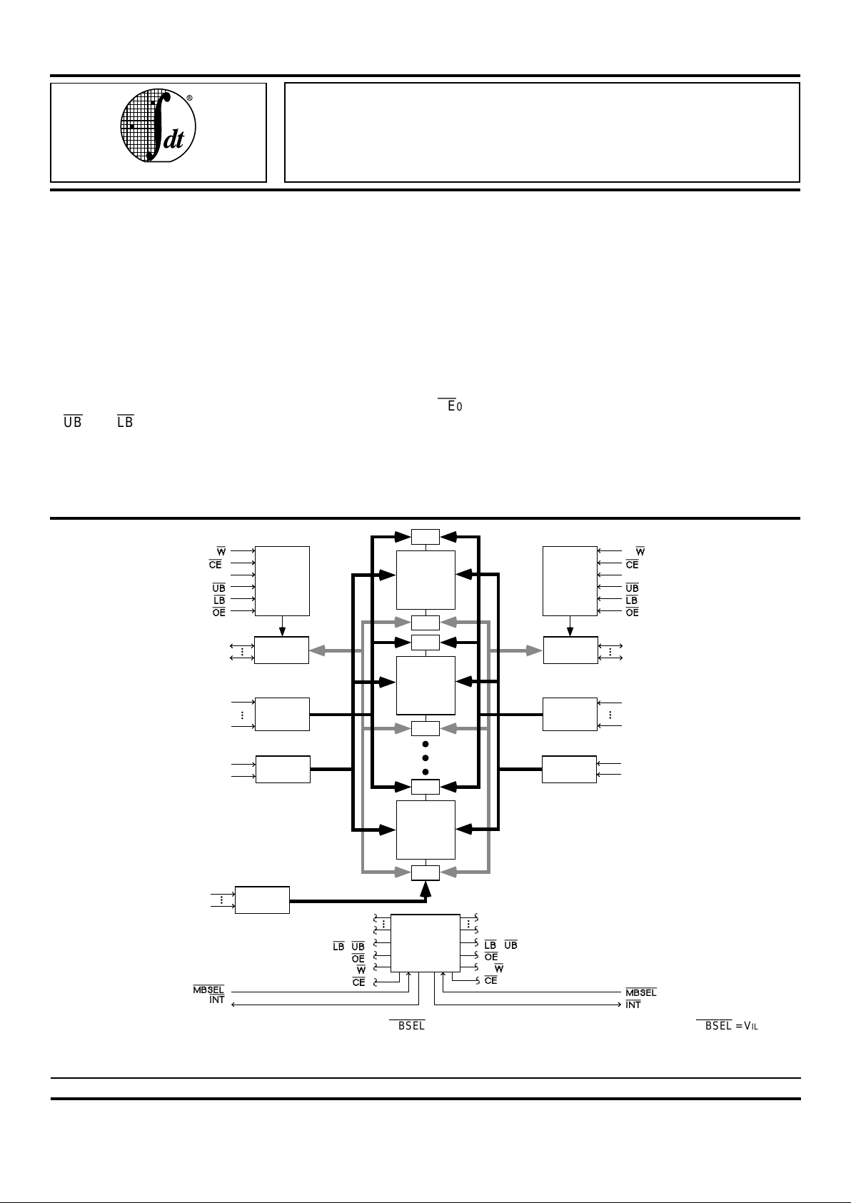
16Kx16
MEMORY
ARRAY
(BANK 3)
MUX
MUX
R/
L
0L
CE
1L
L
L
L
I/O
8L-15L
I/O
0L-7L
A
13L
A
0L
(1)
A
5L
(1)
A
0L
(1)
L/L
L
R/
L
L
MAILBOX
INTERRUPT
LOGIC
16Kx16
MEMORY
ARRAY
(BANK 1)
MUX
MUX
16Kx16
MEMORY
ARRAY
(BANK 0)
MUX
MUX
CONTROL
LOGIC
I/O
CONTROL
BANK
DECODE
ADDRESS
DECODE
R/
R
0R
CE
1R
R
R
R
I/O
8R-15R
I/O
0R-7R
A
13R
A
0R
(1)
CONTROL
LOGIC
I/O
CONTROL
BANK
DECODE
ADDRESS
DECODE
A
5R
(1)
A
0R
(1)
R/R
R
R/
R
R
3592 drw 01
R
R
L
L
BKSEL
3
(2)
BKSEL
0
(2)
BANK
SELECT
BA
1R
BA
0R
BA
1L
BA
0L
FUNCTIONAL BLOCK DIAGRAM
NOTES:
1. The first six address pins for each port serve dual functions. When
MBSEL
= VIH, the pins serve as memory address inputs. When
MBSEL
= VIL, the pins
serve as mailbox address inputs.
2. Each bank has an input pin assigned that allows the user to toggle the assignment of that bank between the two ports. Refer to Table I for more details.
IDT707288S/L
64K x 16 BANK-SWITCHABLE DUAL-PORTED SRAM WITH EXTERNAL BANK SELECTS COMMERCIAL TEMPERATURE RANGE
6.29 2
PIN NAMES
A0 - A13
(1,6)
Address Inputs
BA
0 - BA1
(1)
Bank Address Inputs
MBSEL
(1)
Mailbox Access Control Gate
BKSEL
(2)
Bank Select Inputs
R/
W
(1)
Read/Write Enable
OE
(1)
Output Enable
CE0
, CE1
(1)
Chip Enables
UB, LB
(1)
I/O Byte Enables
I/O
0 – I/O15
(1)
Bidirectional Data Input/Output
INT
(1)
Interrupt Flag (Output)
(3)
VCC
(4)
+5V Power
GND
(5)
Ground
FUNCTIONALITY:
The IDT707288 is a high-speed asynchronous 64K x 16
Bank-Switchable Dual-Ported SRAM, organized in four 16K x
16 banks. The two ports are permitted independent, simultaneous access into separate banks within the shared array.
There are four user-controlled Bank Select input pins , and
each of these pins is associated with a specific bank within the
memory array. Access to a specific bank is gained by placing
the associated Bank Select pin in the appropriate state: VIH
assigns the bank to the left port, and VIL assigns the bank to
the right port (See Truth Table I). Once a bank is assigned to
a particular port, the port has full access to read and write
within that bank. Each port can be assigned as many banks
within the array as needed, up to and including all four banks.
The IDT707288 provides mailboxes to allow inter-processor communications. Each port has four 16-bit mailbox
registers available to which it can write and read and which the
opposite port can read only. These mailboxes are external to
the common SRAM array, and are accessed by setting
MBSEL
= VIL while setting CE = VIH. Each mailbox has an
associated interrupt: a port can generate an interrupt to the
opposite port by writing to the upper byte of any one of its four
16-bit mailboxes. The interrupted port can clear the interrupt
by reading the upper byte. This read will not alter the contents
of the mailbox.
If desired, any source of interrupt can be independently
masked via software. Two registers are provided to permit
interpretation of interrupts: the Interrupt Cause Register and
the Interrupt Status Register. The Interrupt Cause Register
gives the user a snapshot of what has caused the interrupt to
be generated - the specific mailbox written to. The information
in this register provides post-mask signals: Interrupt sources
that have been masked will not be updated. The Interrupt
Status Register gives the user the status of all bits that could
potentially cause an interrupt regardless of whether they have
been masked. Truth Table II gives a detailed explanation of
the use of these registers.
1. All VCC pins must be connected to power supply.
2. All GND pins must be connected to ground supply.
3. This text does not indicate orientation of the actual part-marking.
NOTES:
NOTES:
1. Duplicated per port.
2. Each bank has an input pin assigned that allows the user to toggle the
assignment of that bank between the two ports. Refer to Table I for more
details.
3. Generated upon mailbox access.
4. All Vcc pins must be connected to power supply.
5. All GND pins must be connected to ground supply.
6. The first six address pins for each port serve dual functions. When
MBSEL
= VIH, the pins serve as bank address or memory address inputs. When
MBSEL
= VIL, the pins serve as mailbox address inputs.
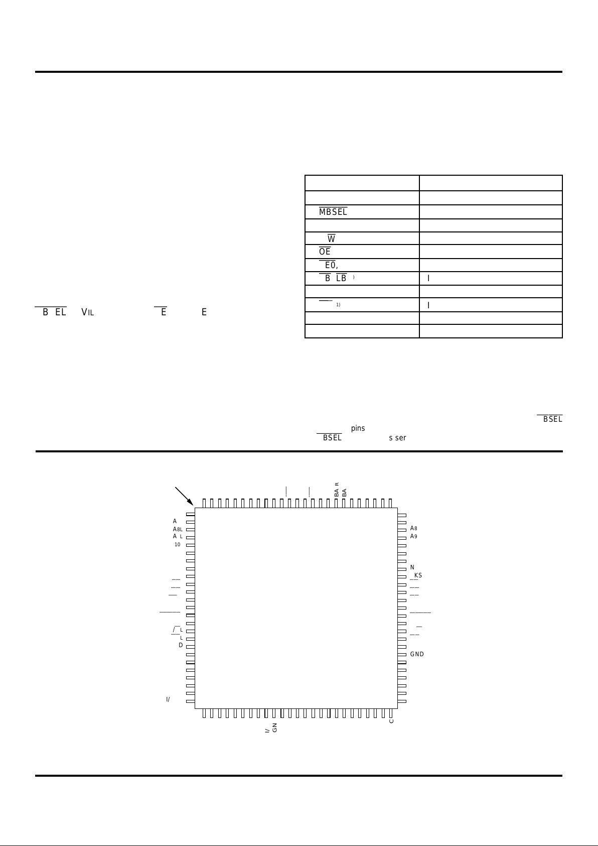
PIN CONFIGURATIONS
(1,2)
3592 tbl 01
INDEX
1
2
3
4
5
6
7
8
9
10
11
12
13
14
15
16
17
18
19
20
21
22
23
24
25
75
74
73
72
71
70
69
68
67
66
65
64
63
62
61
60
59
58
57
56
55
54
53
52
51
26 27 28 29 30 31 32 33 34 35 36 37 38 39 40 41 42 43 44 45 46 47 48 49 50
10099 98 97 96 95 94 93 92 91 90 89 88 87 86 85 84 83 82 81 80 79 78 77 76
IDT707288
PN100-1
100-PIN
TQFP
TOP VIEW
(3)
GND
OE
R
R/
W
R
MBSEL
R
CE
1R
CE
0R
BKSEL
3
NC
GND
A
9R
A
10R
A
8R
A
7R
A
6R
A
11R
I/O
10R
I/O
11R
I/O
12R
I/O
13R
I/O
14R
I/O
15R
GND
UB
R
LB
R
3592 drw 02
I/O
15L
GND
OE
L
R/
W
L
MBSEL
L
CE
1L
CE
0L
Vcc
BKSEL
0
A
11L
A
10L
NC
A
9L
A
8L
A
7L
A
6L
I/O
10L
I/O
11L
I/O
12L
I/O
13L
I/O
14L
UB
L
LB
L
GND
I/O
5R
I/O
4R
I/O
3R
I/O
2R
I/O
0R
I/O
0L
GND
I/O
2L
I/O
4L
I/O
5L
I/O
6L
I/O
7
L
I/O
3L
I/O
1R
I/O
7R
I/O
8R
I/O
9R
I/O
8L
I/O
9L
I/O
6R
A
4R
A
5L
A
4L
A
3R
A
0R
A
12R
INT
R
INT
L
BKSEL
1
A
3L
A
5R
GND
Vcc
I/O1
L
Vcc
GND
A
13R
NC
BA
0RBA1R
A1RA
2R
BKSEL
2
GND
NC
A
0L
A
12L
BA0LBA
1L
A1LA
2L
A
13L

6.29 3
IDT707288S/L
64K x 16 BANK-SWITCHABLE DUAL-PORTED SRAM WITH EXTERNAL BANK SELECTS COMMERCIAL TEMPERATURE RANGE
PIN CONFIGURATIONS (CON'T.)
(1,2)
1. All VCC pins must be connected to power supply.
2. All GND pins must be connected to ground supply.
3. This text does not indicate orientation of the actual part-marking.
NOTES:
3592 drw 03
80 77 74 72 69 68 65 63 60
83 78 76 73 70 67 64 61 5984 56
8687
8890
9192
9495
9796
10099
103101
105104
2
1
5
4
7
8
10
12
13
17
16
21
19
25
22
28
24
32
31 34
35 37
39 40
44 43
48 46
52 49
55 51
IDT707288
G108-1
108-Pin PGA
Top View
ABCDEFGHJKLM
81 57 54
53
82 79 75 71 66 62 58 50
33
36
38
41
42
45
47
369111415182023
29 30
26 27
85
89
93
98
102
106
107
108
12
11
10
09
08
07
06
05
04
03
02
01
I NDEX
(3)
GND
OE
R
R/
W
R
MB
SEL
R
CE
1R
CE
0R
NC
BK
SEL
3
GND
A
9R
A
10R
A
8R
A
7R
A
6R
GND
OE
L
R/
W
L
CE
1L
CE
0L
Vcc
BK
SEL
0
A
11L
A
10L
NC
A
9L
A
8L
A
7L
A
6L
I/O
6R
I/O
5R
I/O
4R
I/O
3R
I/O
2R
I/O
0R
GND
Vcc
I/O
0L
I/O
1L
GNDI/O
2L
I/O
4L
I/O
5L
I/O
6L
I/O7L
I/O
3L
I/O
1R
I/O
7R
NC
I/O
8R
I/O
9R
I/O
8L
I/O
9L
VccA
3R
A
12R
INT
R
INT
L
NC
GND
A
3L
A
5R
A
4R
A
5L
A
4L
A
11R
I/O
10R
I/O
11R
I/O
12R
I/O
13R
I/O
14R
I/O
15R
I/O
10L
I/O
11L
I/O
12L
I/O
13L
I/O
14L
GND
UB
R
LB
R
UB
L
LB
L
GND
NC
NC
NC
NC
NCNC
NC
NC
I/O
15L
BA
1R
BA
0R
A
0R
A
1R
A
2R
A
13R
BK
SEL
2
MB
SEL
L
A
12L
BA
0L
BA
1L
A
0L
A
1L
A
2L
A
13L
BK
SEL
1
GND

IDT707288S/L
64K x 16 BANK-SWITCHABLE DUAL-PORTED SRAM WITH EXTERNAL BANK SELECTS COMMERCIAL TEMPERATURE RANGE
6.29 4
NOTES:
1. Bank 0 refers to the first 16Kx16 memory spaces, Bank 1 to the second
16Kx16 memory spaces, Bank 2 to the third 16Kx16 memory spaces,
and Bank 3 to the fourth 16Kx16 memory spaces. 'LEFT' indicates the
bank is assigned to the left port; 'RIGHT' indicates the bank is assigned
to the right port.
2. The bank select pin inputs must be set at either VIH or VIL - these inputs
are not tri-statable. When changing the bank select inputs (changing
the bank assignments), the device must be write-disabled (CE and/or
R/W set to VIH).
3. 'H' = VIH, 'L' = VIL, 'X' = Don't Care.
ASSIGNING THE BANKS VIA THE EXTERNAL BANK
SELECTS
There are four bank select pins available on the IDT707288,
and each of these pins is associated with a specific bank within
the memory array. The pins are user-controlled inputs:
access to a specific bank is assigned to a particular port by
setting the input to the appropriate level. The process of
assigning the banks is detailed in Truth Table I. Once a bank
is assigned to a port, the owning port has full access to read
and write within that bank. The opposite port is unable to
access that bank until the user reassigns the port. Access by
TRUTH TABLE I –
MEMORY BANK ASSIGNMENT
(
CECE
CECE
CE
AND/OR R/
WW
WW
W
= VIH)
(2,3)
BANK AND
BKSEL0 BKSEL1 BKSEL2 BKSEL3 DIRECTION
(1)
H X X X BANK 0 LEFT
X H X X BANK 1 LEFT
X X H X BANK 2 LEFT
X X X H BANK 3 LEFT
L X X X BANK 0 RIGHT
X L X X BANK 1 RIGHT
X X L X BANK 2 RIGHT
X X X L BANK 3 RIGHT
3592 tbl 02
MAILBOX INTERRUPTS AND INTERRUPT CONTROL
REGISTERS
If the user chooses to use the mailbox interrupt function,
four mailbox locations are assigned to each port. These
mailbox locations are external to the memory array. The
mailboxes are accessed by taking
MBSEL
Low while holding
CE
High.
The mailboxes are 16 bits wide: the message is userdefined since these are addressable SRAM locations. An
interrupt is generated to the opposite port upon writing to the
upper byte of any mailbox location. A port can read the
message it has just written in order to verify it: this read will
not alter the status of the interrupt sent to the opposite port.
The interrupted port can clear the interrupt by reading the
upper byte of the applicable mailbox. This read will not alter
the contents of the mailbox. The use of mailboxes to generate
interrupts to the opposite port and the reading of mailboxes to
clear interrupts is detailed in Truth Table II.
If desired, any of the mailbox interrupts can be independently masked via software. Masking of the interrupt sources
is done in the Mask Register. The masks are individual and
independent: a port can mask any combination of interrupt
sources with no effect on the other sources. Each port can
modify only its own Mask Register. The use of this register is
detailed in Truth Table II.
Two registers are provided to permit interpretation of
interrupts: these are the Interrupt Cause Register and the
Interrupt Status Register. The Interrupt Cause Register gives
the user a snapshot of what has caused the interrupt to be
generated - a specific semaphore granted to that port or a
specific mailbox written to by the opposite port. The information in this register provides post-mask signals: interrupt
sources that have been masked will not be updated. The
Interrupt Status Register gives the user the status of all bits
that could potentially cause an interrupt regardless of whether
they have been masked. The use of the Interrupt Cause
Register and the Interrupt Status Register is detailed in Truth
Table II.
a port to a bank which it does not control will have no effect if
written, and if read unknown values on D0-D15 will be returned.
Each port can be assigned as many banks within the array as
needed, up to and including all four banks.
The bank select pin inputs must be set at either VIH or VIL
- these inputs are not tri-statable. When changing the bank
select inputs (changing the bank assignments), the device
must be write-disabled (CE and/or R/W set to VIH).

6.29 5
IDT707288S/L
64K x 16 BANK-SWITCHABLE DUAL-PORTED SRAM WITH EXTERNAL BANK SELECTS COMMERCIAL TEMPERATURE RANGE
MB
SELR/WUB LB
A5 A4 A3 A2 A1 A0 D0 D1 D2 D3 D4 D5 D6 D7 D8 D9 D10 D11 D12 D13 D14 D15 DESCRIPTION
L X X X L L L L L L RESERVED (7) RESERVED (7)
L X X X RESERVED (7) RESERVED (7)
L(1)(1)(1)HLLLLL XXXXXXXXXXXXXXXX MAILBOX 0 - SET INTERRUPT ON OPPOSITE PORT
L(1)(1)(1)HLLLLHXXXXXXXXXXXXXXXX MAILBOX 1 - SET INTERRUPT ON OPPOSITE PORT
L(1)(1)(1)HLLLHLXXXXXXXXXXXXXXXX MAILBOX 2 - SET INTERRUPT ON OPPOSITE PORT
L(1)(1)(1)HLLLHHXXXXXXXXXXXXXXXX MAILBOX 3 - SET INTERRUPT ON OPPOSITE PORT
H(2)(2)H LLHLLXXXXXXXXXXXXXXXX MAILBOX 0 - CLEAR OPPOSITE PORT INTERRUPT
H(2)(2)H LLHLHXXXXXXXXXXXXXXXX MAILBOX 1 - CLEAR OPPOSITE PORT INTERRUPT
H(2)(2)HLLHHLXXXXXXXXXXXXXXXX MAILBOX 2 - CLEAR OPPOSITE PORT INTERRUPT
H(2)(2)HLLHHHXXXXXXXXXXXXXXXX MAILBOX 3 - CLEAR OPPOSITE PORT INTERRUPT
L (3) (3) (3) H L H L L L (4) (4) (4) (4) (5) (5) (5) (5) (6) (6) (6) (6) X X X X MAILBOX INTERRUPT CONTROLS
L X X X RESERVED (7) RESERVED (7)
L X X X H H H H H H RESERVED (7) RESERVED (7)
3592 tbl 03
TRUTH TABLE II – MAILBOX INTERRUPTS (
CECE
CECE
CE
= VIH)
(8,9)
NOTES:
1. There are four independent mailbox locations available to each side, external to the standard memory array. The mailboxes can be written to in
either 8-bit or 16-bit widths. The upper byte of each mailbox has an associated interrupt to the opposite port. The mailbox interrupts can be
individually masked if desired, and the status of the interrupt determined by polling the Interrupt Status Register (see Note 6 for this table). A port
can read its own mailboxes to verify the data written, without affecting the interrupt which is sent to the opposite port.
2. These registers allow a port to read the data written to a specific mailbox location by the opposite port. Reading the upper byte of the data in a
particular mailbox clears the interrupt associated with that mailbox without modifying the data written. Once the address and R/W are stable, the
actual clearing of the interrupt is triggered by the transition of
MBSEL
from VIH to VIL.
3. This register contains the Mask Register (bits D0-D3), the Interrupt Cause Register (bits D4-D7), and the Interrupt Status Register (bits D8-D11). The
controls for R/W, UB, and LB are manipulated in accordance with the appropriate function. See Notes 4, 5, and 6 for this table. Bits D12-D15 are
"Don't Care".
4. This register, the Mask Register, allows the user to independently mask the various interrupt sources. Writing VIH to the appropriate bit (D0 =
Mailbox 0, D1 = Mailbox 1, D2 = Mailbox 2, and D3 = Mailbox 3) disables the interrupt, while writing VIL enables the interrupt. All four bits in this
register must be written at the same time. This register can be read at any time to verify the mask settings. The masks are individual and
independent: any single interrupt source can be masked with no effect on the other sources. Each port can modify only its own mask settings.
5. This register, the Interrupt Cause Register, gives the user a snapshot of what has caused the interrupt to be generated. Reading VOL for a specific
bit (D4 = Mailbox 0, D5 = Mailbox 1, D6 = Mailbox 2, and D7 = Mailbox 3) indicates that the associated interrupt source has generated an interrupt.
Acknowledging the interrupt clears the bit in this register (see Note 2 for this table). This register provides post-mask information: if the interrupt
source has been masked, the associated bit in this register will not update.
6. This register, the Interrupt Status Register, gives the user the status of all interrupt sources that could potentially cause an interrupt regardless of
whether they have been masked. Reading VOL for a specific bit (D8 = Mailbox 0, D9 = Mailbox 1, D10 = Mailbox 2, and D11 = Mailbox 3) indicates
that the associated interrupt source has generated an interrupt. Acknowledging the interrupt clears the associated bit in this register (see Note 2 for
this table). This register provides pre-mask information: regardless of whether an interrupt source has been masked, the associated bit in this
register will update.
7. Access to registers defined as "RESERVED" will have no effect, if written, and if read unknown values on D0-D15 will be returned.
8. These registers are not guaranteed to initialize in any known state. At power-up, the initialization sequence should include the set-up of these
registers.
9. 'L' = VIL or VOL, 'H' = VIH or VOH, 'X' = Don't Care.

IDT707288S/L
64K x 16 BANK-SWITCHABLE DUAL-PORTED SRAM WITH EXTERNAL BANK SELECTS COMMERCIAL TEMPERATURE RANGE
6.29 6
ORDERING INFORMATION
A
Power
999
SpeedAPackage
A
Process/
Temperature
Range
Blank
Commercial (0°C to +70°C)
PF
G
100-pin TQFP (PN100-1)
108-pin PGA (G108-1)
20
25
S
L
Standard Power
Low Power
XXXXX
Device
Type
1Mbit (4 x 16K x 16)
Bank-Switchable Dual-Ported SRAM
with External Bank Selects
707288
IDT
3592 drw 19
Commercial Only
Commercial Only
Speed in nanoseconds
 Loading...