

Page 1
Integrated Device Technology, Inc.
W
CMOS STATIC RAM
256K (64K x 4-BIT)
IDT61298SA
FEATURES:
• 64K x 4 high-speed static RAM
• Fast Output Enable (OE) pin available for added system
flexibility
• High speed (equal access and cycle times)
— Commercial: 12/15 ns (max.)
• JEDEC standard pinout
• 300 mil 28-pin SOJ
• Produced with advanced CMOS technology
• Bidirectional data inputs and outputs
• Inputs/Outputs TTL-compatible
• Three-state outputs
• Military product compliant to MIL-STD-883, Class B
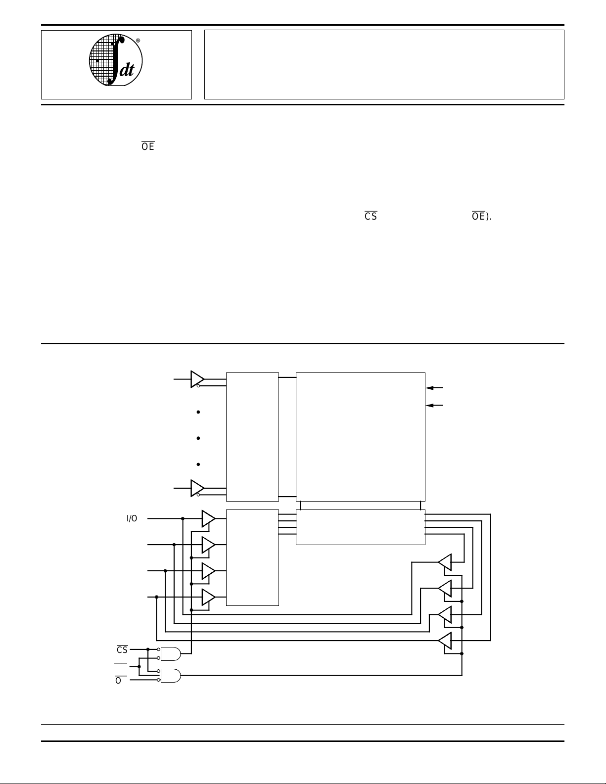
FUNCTIONAL BLOCK DIAGRAM
A0
D
E
C
O
D
E
R
DESCRIPTION:
The lDT61298SA is a 262,144-bit high-speed static RAM
organized as 64K x 4. It is fabricated using IDT’s highperformance, high-reliability CMOS technology. This state-ofthe-art technology, combined with innovative circuit design
techniques, provides a cost-effective approach for memory
intensive applications.
The IDT61298SA features two memory control functions:
Chip Select (CS) and Output Enable (OE). These two functions greatly enhance the IDT61298SA's overall flexibility in
high-speed memory applications.
Access times as fast as 12ns are available. The IDT61298SA
offers a reduced power standby mode, I
the designer to considerably reduce device power requirements. This capability significantly decreases system power
and cooling levels, while greatly enhancing system reliability.
All inputs and outputs are TTL-compatible and the device
operates from a single 5 volt supply. Fully static asynchronous
VCC
GND
262,144-BIT
MEMORY ARRAY
SB1, which enables
A15
I/O0
I/O1
I/O2
I/O3
CS
E
OE
The IDT logo is a registered trademark of Integrated Device Technology, Inc.
INPUT
DATA
CONTROL
I/O CONTROL
2971 drw 01
COMMERCIAL TEMPERATURE RANGES MAY 1996
1996 Integrated Device Technology, Inc. DSC-2971/6
7.1
1
Page 2
IDT61298SA
CMOS STATIC RAM 256K (64K x 4-BIT) COMMERCIAL TEMPERATURE RANGE
DESCRIPTION (Continued)
circuitry, along with matching access and cycle times, favor
the simplified system design approach.
The IDT61298SA is packaged in a 300 mil, 28-pin SOJ,
providing improved board-level packing densities.
PIN CONFIGURATION
NC
A
A
A
A
A
A
A
A
A
A
CS
OE
GND
0
1
2
3
4
5
6
7
8
9
1
2
3
4
5
6
7
SO28-5
8
9
10
11
12
13
14
SOJ
TOP VIEW
28
27
26
25
24
23
22
21
20
19
18
17
16
15
V
CC
A
15
A
14
A
13
A
12
A
11
A
10
NC
NC
3
I/O
I/O
2
I/O
1
I/O
0
WE
2971 drw 02
TRUTH TABLE
(1,2)
CSCSOEOEWEWE I/O Function
L L H DATA
L X L DATA
OUT Read Data
IN Write Data
L H H High-Z Outputs Disabled
H X X High-Z Deselected - Standby (I
(3)
V
HC
NOTES: 2971 tbl 01
1. H = VIH, L = VIL, x = Don't care.
2. V
3. Other inputs ≥V
ABSOLUTE MAXIMUM RATINGS
X X High-Z Deselected - Standby (ISB1)
LC = 0.2V, VHC = VCC -0.2V.
HC or ≤VLC.
(1)
SB)
Symbol Rating Com’l. Unit
(2)
V
TERM
Terminal Voltage –0.5 to +7.0 V
with Respect
to GND
A Operating 0 to +70 °C
T
Temperature
BIAS Temperature –55 to +125 °C
T
Under Bias
STG Storage –55 to +125 °C
T
Temperature
PT Power Dissipation 1.0 W
I
OUT DC Output 50 mA
Current
NOTES: 2971 tbl 02
1. Stresses greater than those listed under ABSOLUTE MAXIMUM
RATINGS may cause permanent damage to the device. This is a stress
rating only and functional operation of the device at these or any other
conditions above those indicated in the operational sections of this
specification is not implied. Exposure to absolute maximum rating
conditions for extended periods may affect reliability.
TERM must not exceed VCC + 0.5V.
2. V
PIN DESCRIPTIONS
Name Description
A
0–A14 Addresses
I/O
0–I/O7 Data Input/Output
CS
WE
OE
GND Ground
V
CC Power
Chip Select
Write Enable
Output Enable
CAPACITANCE
(TA = +25°C, f = 1.0MHz, SOJ Package)
Symbol Parameter
CIN Input Capacitance V IN = 3dV 5 pF
I/O I/O Capacitance VOUT = 3dV 7 pF
C
NOTE: 2971 tbl 03
1. This parameter is determined by device characterization, but is not
2971 tbl 04
production tested.
7.1 2
(1)
Conditions Max. Unit
Page 3
IDT61298SA
CMOS STATIC RAM 256K (64K x 4-BIT) COMMERCIAL TEMPERATURE RANGE
RECOMMENDED OPERATING
TEMPERATURE AND SUPPLY VOLTAGE
Grade Temperature GND Vcc
RECOMMENDED DC OPERATING
CONDITIONS
Symbol Parameter Min. Typ. Max. Unit
VCC Supply Voltage 4.5 5.0 5.5 V
Commercial 0°C to +70°C 0V 5V ± 10%
DC ELECTRICAL CHARACTERISTICS
(1)
2971 tbl 05
GND Supply Voltage 0 0 0 V
VIH Input High Voltage 2.2 — VCC + 0.5V V
IL Input Low Voltage –0.5
V
NOTE: 2971 tbl 06
1. VIL (min.) = –1.5V for pulse width less than 10ns, once per cycle.
(1)
— 0.8 V
(VCC = 5V ± 10%, VLC = 0.2V, VHC = VCC - 0.2V)
61298SA12 61298SA15
Symbol Parameter
CC Dynamic Operating Current
I
CS
= V
IL, Outputs Open 160 — 140 — mA
V
CC = Max., f = fMAX
(2)
ISB Standby Power Supply
Current (TTL Level) 50 — 45 — mA
CS
≥ V
IH, VCC = Max.,
Outputs Open, f = f
MAX
(2)
ISB1 Full Standby Power
Supply Current (CMOS Level) 20 — 20 — mA
CS
≥ V
HC, VCC = Max.,
(2),
f = 0
NOTES: 2971 tbl 07
1. All values are maximum guaranteed values.
MAX = 1/tRC (all address inputs are cycling at fMAX); f = 0 means no address input lines are changing.
2. f
VLC ≥ VIN ≥ VHC
Com’l. Mil. Com’l. Mil. Unit
AC TEST CONDITIONS
Input Pulse Levels GND to 3.0V
Input Rise/Fall Times 3ns
Input Timing Reference Levels 1.5V
Output Reference Levels 1.5V
AC Test Load See Figures 1 and 2
5V
480
Ω
DATA
OUT
255
Ω
Figure 1. AC Test Load Figure 2. AC Test Load
30pF*
2971 drw 03
*Includes scope and jig capacitances
2971 tbl 08
DATA
5V
OUT
255Ω
CLZ, tOLZ, tCHZ, tOHZ, tOW, tWHZ)
(for t
480Ω
5pF*
2971 drw 04
7.1 3
Page 4

IDT61298SA
CMOS STATIC RAM 256K (64K x 4-BIT) COMMERCIAL TEMPERATURE RANGE
DC ELECTRICAL CHARACTERISTICS
VCC = 5.0V ± 10%
IDT61298SA
Symbol Parameter Test Condition Min. Typ. Max. Unit
LI| Input Leakage Current VCC = Max., µA
|I
VIN = GND to VCC —— 5
LO| Output Leakage Current VCC = Max., CS = VIH, µA
|I
VOUT = GND to VCC —— 5
V
OL Output Low Voltage IOL = 8mA, VCC = Min. — — 0.4 V
IOL = 10mA, VCC = Min. — — 0.5
OH Output High Voltage IOH = –4mA, VCC = Min. 2.4 — — V
V
2971 tbl 09
AC ELECTRICAL CHARACTERISTICS (VCC = 5.0V ± 10%)
61298SA12 61298SA15
Symbol Parameter Min. Max. Min. Max. Unit
Read Cycle
t
RC Read Cycle Time 12 — 15 — ns
AA Address Access Time — 12 — 15 ns
t
t
ACS Chip Select Access Time — 12 — 15 ns
(1)
t
CLZ
t
CHZ
t
OE Output Enable to Output Valid — 6 — 7 ns
t
OLZ
t
OHZ
t
OH Output Hold from Address Change 3 — 3 — ns
(1)
t
PU
(1)
t
PD
Write Cycle
t
WC Write Cycle Time 12 — 15 — ns
t
CW Chip Select to End-of-Write 9 — 10 — ns
t
AW Address Valid to End-of-Write 9 — 10 — ns
t
AS Address Set-up Time 0 — 0 — ns
t
WP Write Pulse Width 9 — 10 — ns
t
WR Write Recovery Time 0 — 0 — ns
t
DW Data Valid to End-of-Write 6 — 7 — ns
t
DH Data Hold Time 0 — 0 — ns
t
WHZ
t
OW
NOTES: 2971 tbl 10
1. This parameter is guaranteed with AC test load (Figure 2) by device characterization, but is not production tested.
Chip Select to Output in Low-Z 4 — 4 — ns
(1)
Chip Deselect to Output in High-Z — 6 — 7 ns
(1)
Output Enable to Output in Low-Z 0 — 0 — ns
(1)
Output Disable to Output in High-Z — 6 — 6 ns
Chip Select to Power-Up Time 0 — 0 — ns
Chip Deselect to Power-Down Time — 12 — 15 ns
(1)
Write Enable to Output in High-Z — 6 — 6 ns
(1)
Output Active from End-of-Write 4 — 4 — ns
7.1 4
Page 5

IDT61298SA
CMOS STATIC RAM 256K (64K x 4-BIT) COMMERCIAL TEMPERATURE RANGE
TIMING WAVEFORM OF READ CYCLE NO. 1
tRC
ADDRESS
tAA tOH
OE
tOE
(5)
tOLZ
CS
tACS
(5)
tCLZ
OUT
DATA
TIMING WAVEFORM OF READ CYCLE NO. 2
tRC
(1)
(1,2,4)
DATA VALID
tOHZ
tCHZ
(5)
(5)
2971 drw 05
ADDRESS
tAA
tOH
DATA
OUT
TIMING WAVEFORM OF READ CYCLE NO. 3
CS
tACS
(5)
tCLZ
DATAOUT
t PU
V
CC
SUPPLY
CURRENT
NOTES:
1.WE is HIGH for Read cycle.
2. Device is continuously selected, CS is LOW.
3. Address valid prior to or coincident with CS transition LOW.
4.OE is LOW.
5. Transition is measured ±200mV from steady state.
ICC
ISB
(1,3,4)
DATA VALID
DATA VALID
tOH
tPD
2971 drw 06
(5)
CHZt
2971 drw 07
7.1 5
Page 6

IDT61298SA
CMOS STATIC RAM 256K (64K x 4-BIT) COMMERCIAL TEMPERATURE RANGE
TIMING WAVEFORM OF WRITE CYCLE NO. 1 (
tWC
ADDRESS
tAW
CS
tAS tWP tWR
WE
(6)
tWHZ
DATAOUT
(4)
DATAIN
TIMING WAVEFORM OF WRITE CYCLE NO. 2 (
WEWE CONTROLLED TIMING)
(3)
(6)
tOW
tDW tDH
DATA VALID
CSCS CONTROLLED TIMING)
(1,2,3,5)
(4)
2971 drw 08
(1,2,5)
tWC
ADDRESS
tAW
CS
tAS
tCW
tWR
WE
tDW tDH
DATAIN
NOTES:
1.WE or CS must be HIGH during all address transitions.
2. A write occurs during the overlap of a LOW CS and a LOW WE.
3.OE is continuously HIGH. If OE is LOW during a WE controlled write cycle, the write pulse width must be the greater than or equal to t
the I/O drivers to turn off and data to be placed on the bus for the required t
not apply and the minimum write pulse is as short as the spectified t
4. During this period, I/O pins are in the output state so that the input signals must not be applied.
5. If the CS LOW transition occurs simultaneously with or after the WE LOW transition, the outputs remain in a high-impedance state.
6. Transition is measured ±200mV from steady state.
WP.
DW. If
OE
is HIGH during a WE controlled write cycle, this requirement does
DATA VALID
2971 drw 09
WHZ + tDW to allow
7.1 6
Page 7

IDT61298SA
CMOS STATIC RAM 256K (64K x 4-BIT) COMMERCIAL TEMPERATURE RANGE
ORDERING INFORMATION
IDT
61298
Device
Type
SA
PowerXXSpeedXXPackage
X
Process/
Temperature
Range
Blank Commercial (0°C to +70°C)
Y
12
15
300-mil SOJ (SO28-5)
Commercial Only
Commercial Only
Speed in nanoseconds
2971 drw 10
7.1 7
 Loading...