

查询IDT54FCT2646ATD供应商
FAST CMOS OCTAL
TRANSCEIVER/
REGISTERS (3-STATE)
Integrated Device Technology, Inc.
FEATURES:
• Common features:
– Low input and output leakage ≤1µA (max.)
– Extended commercial range of –40°C to +85°C
– CMOS power levels
– True TTL input and output compatibility
– V
OH = 3.3V (typ.)
– VOL = 0.3V (typ.)
– Meets or exceeds JEDEC standard 18 specifications
– Product available in Radiation Tolerant and Radiation
Enhanced versions
– Military product compliant to MIL-STD-883, Class B
and DESC listed (dual marked)
– Available in DIP, SOIC, SSOP, QSOP, TSSOP,
CERPACK and LCC packages
• Features for FCT646T/648T/652T:
– Std., A, C and D speed grades
– High drive outputs (-15mA IOH, 64mA IOL)
– Power off disable outputs permit “live insertion”
• Features for FCT2646T/2652T:
– Std., A, and C speed grades
– Resistor outputs (-15mA IOH, 12mA IOL Com.)
(-12mA IOH, 12mA IOL Mil.)
– Reduced system switching noise
IDT54/74FCT646T/AT/CT/DT - 2646T/AT/CT
IDT54/74FCT648T/AT/CT
IDT54/74FCT652T/AT/CT/DT - 2652T/AT/CT
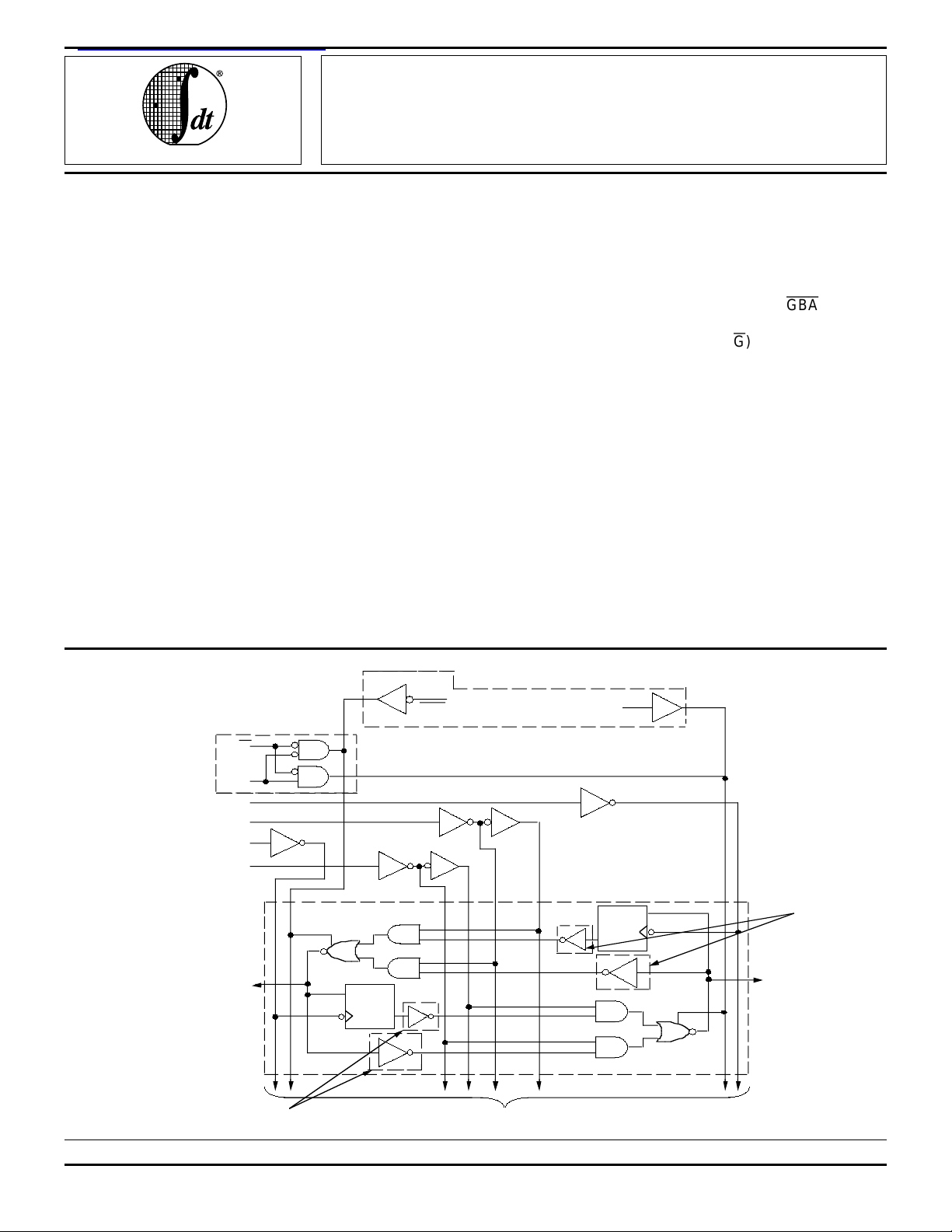
DESCRIPTION:
The FCT646T/FCT2646T/FCT648T/FCT652T/2652T consist of a bus transceiver with 3-state D-type flip-flops and
control circuitry arranged for multiplexed transmission of data
directly from the data bus or from the internal storage registers.
The FCT652T/FCT2652T utilize GAB and
control the transceiver functions. The FCT646T/FCT2646T/
FCT648T utilize the enable control (G) and direction (DIR)
pins to control the transceiver functions.
SAB and SBA control pins are provided to select either realtime or stored data transfer. The circuitry used for select
control will eliminate the typical decoding glitch that occurs in
a multiplexer during the transition between stored and realtime data. A LOW input level selects real-time data and a
HIGH selects stored data.
Data on the A or B data bus, or both, can be stored in the
internal D flip-flops by LOW-to-HIGH transitions at the appropriate clock pins (CPAB or CPBA), regardless of the select or
enable control pins.
The FCT26xxT have balanced drive outputs with current
limiting resistors. This offers low ground bounce, minimal
undershoot and controlled output fall times-reducing the need
for external series terminating resistors. FCT2xxxT parts are
plug-in replacements for FCTxxxT parts.
GBA
signals to
FUNCTIONAL BLOCK DIAGRAM
IDT54/74FCT646/2646/648
646/2646/652/2652
The IDT logo is a registered trademark of Integrated Device Technology, Inc.
DIR
CPBA
SBA
CPAB
SAB
ONLY
ONLY
G
A1
1 OF 8 CHANNELS
A REG
1D
C1
GBA
TO 7 OTHER CHANNELS
IDT54/74FCT652/2652
ONLY
GAB
B REG
C1
1D
646/2646/652/2652
ONLY
B1
2634 drw 01
MILITARY AND COMMERCIAL TEMPERATURE RANGES SEPTEMBER 1996
1996 Integrated Device Technology, Inc. 6.20 DSC-2634/9
1

IDT54/74FCT646/2646/652/2652T/AT/CT/DT, 648T/AT/CT
FAST CMOS OCTAL TRANSCEIVER/REGISTER MILITARY AND COMMERCIAL TEMPERATURE RANGES
PIN CONFIGURATIONS
CPAB
SAB
DIR
GND
CPAB
SAB
GAB
GND
2
3
P24-1
4
A
A2
A3
A4
A5
A6
A
A8
1
7
5
6
7
8
9
10
11
D24-1
SO24-2
SO24-7*
SO24-8
SO24-9*
&
E24-1
12
DIP/SOIC/SSOP/
QSOP/TSSOP/CERPACK
TOP VIEW
* FCT646/2646T/AT/CT/DT only
2
3
P24-1
4
A
A2
A3
A4
A5
A6
A
A8
1
7
5
6
7
8
9
10
11
D24-1
SO24-2
SO24-7*
SO24-8
&
E24-1
12
DIP/SOIC/SSOP/
QSOP/CERPACK
TOP VIEW
* FCT652/2652T/AT/CT/DT only
24
23
22
21
20
19
18
17
16
15
14
13
24
23
22
21
20
19
18
17
16
15
14
13
VCC1
CPBA
SBA
G
B
1
B2
B3
B4
B5
B6
B7
8
B
2634 drw 02
VCC1
CPBA
SBA
GBA
B
1
B2
B3
B4
B5
B6
B7
8
B
2634 drw 04
FCT646/FCT2646T
FCT648
FCT652/FCT2652T
INDEX
INDEX
NC
A1
A2
A3
NC
A
A5
A6
A1
A2
A3
A
A5
A6
CPAB
1
L28-1
15
GND
LCC
CPAB
1
L28-1
15
GND
LCC
NC
NC
NC
NC
CC
V
8
B
CC
V
8
B
CPBA
SBA
262728
25
24
23
22
21
20
19
181716
B7
B6
CPBA
SBA
262728
25
24
23
22
21
20
19
181716
B7
B6
G
1
B
B2
NC
3
B
B4
B5
2634 drw 03
GBA
B
1
B2
NC
B
3
B4
B5
2634 drw 05
SAB
DIR
32
4
5
6
7
8
4
9
10
11
5
6
7
8
4
9
10
11
1213
7
A
GAB
4
1213
7
A
32
14
A8
TOP VIEW
SAB
14
A8
TOP VIEW
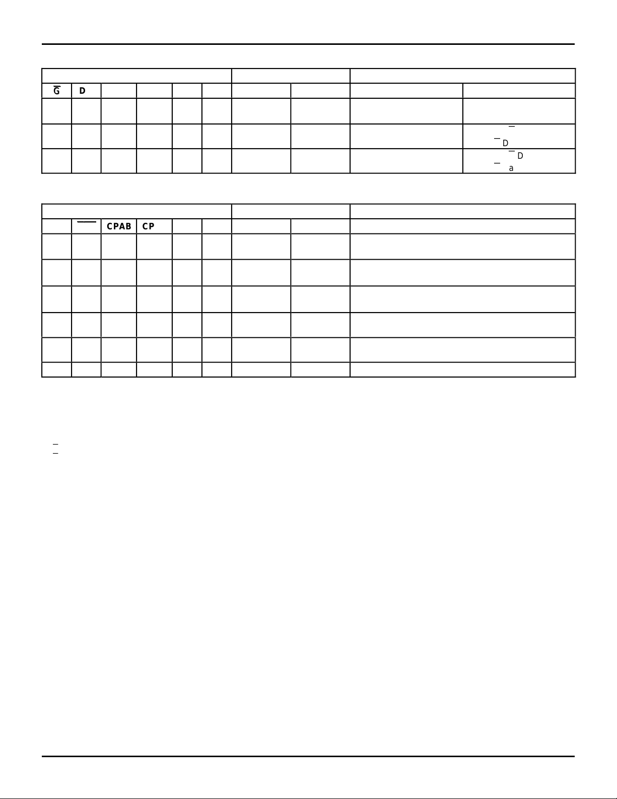
PIN DESCRIPTION
Pin Names Description
A1 - A
8
B1 - B
8
CPAB, CPBA Clock Pulse Inputs
SAB, SBA Output Data Source Select Inputs
DIR,
G
GAB,
GBA
6.20 2
Data Register A Inputs
Data Register B Outputs
Data Register B Inputs
Data Register A Outputs
Output Enable Inputs (646/648)
Output Enable Inputs (652)
2634 tbl 01
IDT54/74FCT646/2646/652/2652T/AT/CT/DT, 648T/AT/CT
FAST CMOS OCTAL TRANSCEIVER/REGISTER MILITARY AND COMMERCIAL TEMPERATURE RANGES
FUNCTION TABLE (646/648)
Inputs Data I/O
GGDIR CPAB CPBA SAB SBA A1 - A8 B1 - B8 FCT646T/FCT2646T FCT648T
H
XXH or L↑H or L↑X
H
L
L
L
L
L
L
H
HXH or L
X
X
X
H or LXX
X
X
X
X
X
L
Input Input Isolation
Output Input Real-Time B Data to A Bus
H
L
X
H
X
Input Output Real-Time A Data to B Bus
(1)
Operation or Function
Store A and B Data
Stored B Data to A Bus
Stored A Data to B Bus
Isolation
Store A and B Data
Real-Time B Data to A Bus
Stored B Data to A Bus
Real-Time A Data to B Bus
Stored A Data to B Bus
2634 tbl 02
FUNCTION TABLE (652)
Inputs Data I/O Operation or Function
GAB
NOTES: 2634 tbl 03
1. The data output functions may be enabled or disabled by various signals at the GAB or GBA inputs. Data
2. Select control = L: clocks can occur simultaneously.
3.A in B Register.
4.B in A Register.
GBA
CPAB CPBA SAB SBA A1 - A8 B1 - B8 FCT652T/FCT2652T
GBA
L
HHH or L↑H or L↑X
L
X
H
L
L
L
L
H
H
H
H
XLH or L
L
L
H
HXH or L
↑
↑
↑
X
X
H or L↑X
X
↑
↑
X
H or LXX
X
X
X
(2)
X
XXX
L
H
X
X
X
X
(2)
L
H
X
X
Input Input Isolation
Store A and B Data
Input
Input
(1)
Store A, Hold B
Store A in Both Registers
Hold A, Store B
Store B in Both Registers
Input
Input
Unspecified
Output
Unspecified
Output
(1)
Output Input Real-Time B Data to A Bus
Stored B Data to A Bus
Input Output Real-Time A Data to B Bus
Stored A Data to B Bus
H L H or L H or L H H Output Output Stored A Data to B Bus and Stored B Data to A Bus
input functions are always enabled, i.e. data at the bus pins will be stored on every LOW-to-HIGH transition
on the clock inputs.
Select control = H: clocks must be staggered in order to load both registers.
H = HIGH, L = LOW, X = Don't Care, ≠ = LOW-to-HIGH transition.
6.20 3

IDT54/74FCT646/2646/652/2652T/AT/CT/DT, 648T/AT/CT
FAST CMOS OCTAL TRANSCEIVER/REGISTER MILITARY AND COMMERCIAL TEMPERATURE RANGES
652/2652
646/2646/
648
BUS
A
BUS
B
GAB GBA CPAB CPBA SAB SBA
LL X X XL
DIR G CPAB CPBA SAB SBA
LL X X XL
REAL-TIME TRANSFER
BUS
A
BUS B TO A
BUS
B
2634 drw 06
652/2652
646/2646/
648
BUS
A
BUS
B
GAB GBA CPAB CPBA SAB SBA
HH
X
XLX
DIR G CPAB CPBA SAB SBA
HL X X L X
REAL-TIME TRANSFER
BUS
A
BUS A TO B
BUS
B
2634 drw 07
652/2652 GAB GBA CPAB CPBA SAB SBA
646/2646/
648
XH
↑
LX X
LH
↑↑
DIR G CPAB CPBA SAB SBA
HL
↑
LL X
XH
STORAGE FROM
↑↑
A AND/OR B
XXX
↑
XX
XX
XXX
↑
XX
XX
2634 drw 08
652/2652 GAB GBA CPAB CPBA SAB SBA
H L H or H or H H
646/2646/
648
(1)
DIR G CPAB CPBA SAB SBA
L L X H or X H
H L H or X H X
TRANSFER STORES
DATA TO A AND/OR B
2634 drw 09
NOTE:
1. 646/2646/648 cannot transfer data to A bus and B bus simultaneously.
6.20 4

IDT54/74FCT646/2646/652/2652T/AT/CT/DT, 648T/AT/CT
FAST CMOS OCTAL TRANSCEIVER/REGISTER MILITARY AND COMMERCIAL TEMPERATURE RANGES
(1)
Symbol Description Max. Unit
(2)
V
TERM
Terminal Voltage with Respect to
–0.5 to +7.0 V
GND
(3)
V
TERM
T
STG
I
OUT
NOTES:
1. Stresses greater than those listed under ABSOLUTE MAXIMUM RATINGS may cause permanent damage to the device. This is a stress rating
only and functional operation of the device at these or any other conditions
above those indicated in the operational sections of this specification is
not implied. Exposure to absolute maximum rating conditions for
extended periods may affect reliability. No terminal voltage may exceed
V
2. Input and V
3. Outputs and I/O terminals only.
Terminal Voltage with Respect to
GND
–0.5 to
V
Storage Temperature –65 to +150°C
DC Output Current –60 to +120 mA
CC by +0.5V unless otherwise noted.
CC terminals only.
CC
+0.5
2634 lnk 04
CAPACITANCE (TA = +25°C, f = 1.0MHz)ABSOLUTE MAXIMUM RATINGS
Symbol Parameter
CIN Input
Capacitance
V
COUT Output
Capacitance
NOTE:
1. This parameter is measured at characterization but not tested.
(1)
Conditions Typ. Max. Unit
VIN = 0V 6 10 pF
VOUT = 0V 8 12 pF
DC ELECTRICAL CHARACTERISTICS OVER OPERATING RANGE
Following Conditions Apply Unless Otherwise Specified:
Commercial: TA = –40°C to +85°C, VCC = 5.0V ± 5%; Military: TA = –55°C to +125°C, VCC = 5.0V ± 10%
Symbol Parameter Test Conditions
(1)
Min. Typ.
VIH Input HIGH Level Guaranteed Logic HIGH Level 2.0 — — V
VIL Input LOW Level Guaranteed Logic LOW Level — — 0.8 V
II H Input HIGH Current
II L Input LOW Current
(4)
(4)
VI = 0.5V — — ±1
VCC = Max. VI = 2.7V — — ±1 µA
IOZH High Impedance Output Current VCC = Max. VO = 2.7V — — ±1 µA
(4)
(4)
VO = 0.5V — — ±1
VCC = Max., VI = VCC (Max.) — — ±1 µA
IOZL (3-State Output pins)
II Input HIGH Current
VIK Clamp Diode Voltage VCC = Min., IIN = –18mA — –0.7 –1.2 V
VH Input Hysteresis — — 200 — mV
ICC Quiescent Power Supply Current VCC = Max., VIN = GND or VCC — 0.01 1 mA
(2)
Max. Unit
OUTPUT DRIVE CHARACTERISTICS FOR FCT646T/648T/652T
Symbol Parameter Test Conditions
VOH Output HIGH Voltage VCC = Min.
IN = VIH or VIL
V
IOH = –6mA MIL.
OH = –8mA COM'L.
I
IOH = –12mA MIL.
OH = –15mA COM'L.
I
VOL Output LOW Voltage VCC = Min.
IN = VIH or VIL
V
IOS Short Circuit Current VCC = Max., VO = GND
IOFF Input/Output Power Off Leakage
(5)
VCC = 0V, VIN or VO ≤ 4.5V — — ±1 µA
IOL = 48mA MIL.
OL = 64mA COM'L.
I
(3)
(1)
Min. Typ.
2.4 3.3 — V
2.0 3.0 — V
— 0.3 0.55 V
–60 –120 –225 mA
(2)
Max. Unit
2634 lnk 05
2634 lnk 05
2634 lnk 06
6.20 5

IDT54/74FCT646/2646/652/2652T/AT/CT/DT, 648T/AT/CT
FAST CMOS OCTAL TRANSCEIVER/REGISTER MILITARY AND COMMERCIAL TEMPERATURE RANGES
OUTPUT DRIVE CHARACTERISTICS FOR FCT2646T/2652T
Symbol Parameter Test Conditions
IODL Output LOW Current VCC = 5V, VIN = VIH or VIL, VOUT = 1.5V
IODH Output HIGH Current VCC = 5V, VIN = VIH or V IL, VOUT = 1.5V
VOH Output HIGH Voltage VCC = Min.
V
IN = VIH or VIL
VOL Output LOW Voltage VCC = Min.
V
IN = VIH or VIL
NOTES:
1. For conditions shown as Max. or Min., use appropriate value specified under Electrical Characteristics for the applicable device type.
2. Typical values are at Vcc = 5.0V, +25°C ambient.
3. Not more than one output should be shorted at one time. Duration of the short circuit test should not exceed one second.
4. The test limit for this parameter is ±5µA at T
5. This parameter is guaranteed but not tested.
A = –55°C.
(1)
(3)
(3)
IOH = –12mA MIL.
I
OH = –15mA COM'L.
Min. Typ.
16 48 — mA
–16 –48 — mA
2.4 3.3 — V
IOL = 12mA — 0.3 0.50 V
(2)
Max. Unit
2634 lnk 07
POWER SUPPLY CHARACTERISTICS
Symbol Parameter Test Conditions
∆ICC Quiescent Power Supply Current
TTL Inputs HIGH
ICCD Dynamic Power Supply Current
VCC = Max.
V
(4)
VCC = Max.
IN = 3.4V
(3)
Outputs Open
GAB =
GBA
= GND or
G
= DIR = GND
(1)
IN = VCC
V
VIN = GND
Min. Typ.
— 0.5 2.0 mA
FCTxxxT — 0.15 0.25 mA/
FCT2xxxT — 0.06 0.12
One Input Toggling
50% Duty Cycle
IC Total Power Supply Current
(6)
VCC = Max.
Outputs Open
fCP = 10MHz
VIN = VCC
VIN = GND
FCTxxxT — 1.5 3.5 mA
FCT2xxxT — 0.6 2.2
50% Duty Cycle
GAB =
GBA
= GND or
G
= DIR = GND
One Bit Toggling
VIN = 3.4
IN = GND
V
FCTxxxT — 2.0 5.5
FCT2xxxT 1.1 4.2
at fi = 5MHz
50% Duty Cycle
VCC = Max.
Outputs Open
fCP = 10MHz
VIN = VCC
VIN = GND
FCTxxxT — 3.8 7.3
FCT2xxxT — 1.5 4.0
50% Duty Cycle
GAB =
GBA
= GND or
G
= DIR = GND
Eight Bits Toggling
V
IN = 3.4
IN = GND
V
FCTxxxT — 6.0 16.3
FCT2xxxT — 3.8 13.0
at fi = 2.5MHz
50% Duty Cycle
NOTES:
1. For conditions shown as Max. or Min., use appropriate value specified under Electrical Characteristics for the applicable device type.
2. Typical values are at V
3. Per TTL driven input (V
4. This parameter is not directly testable, but is derived for use in Total Power Supply Calculations.
5. Values for these conditions are examples of the I
C = IQUIESCENT + IINPUTS + IDYNAMIC
6. I
IC = ICC + ∆ICC DHNT + ICCD (fCP/2 + fiNi)
CC = Quiescent Current
I
CC = Power Supply Current for a TTL High Input (VIN = 3.4V)
∆I
H = Duty Cycle for TTL Inputs High
D
T = Number of TTL Inputs at DH
N
ICCD = Dynamic Current Caused by an Input Transition Pair (HLH or LHL)
CP = Clock Frequency for Register Devices (Zero for Non-Register Devices)
f
i = Input Frequency
f
i = Number of Inputs at fi
N
All currents are in milliamps and all frequencies are in megahertz.
CC = 5.0V, +25°C ambient.
IN = 3.4V). All other inputs at VCC or GND.
CC formula. These limits are guaranteed but not tested.
(2)
Max. Unit
MHz
(5)
(5)
(5)
(5)
2634 tbl 08
6.20 6

IDT54/74FCT646/2646/652/2652T/AT/CT/DT, 648T/AT/CT
FAST CMOS OCTAL TRANSCEIVER/REGISTER MILITARY AND COMMERCIAL TEMPERATURE RANGES
SWITCHING CHARACTERISTICS OVER OPERATING RANGE
646/648/652T
2646/2652T
Com'l. Mil. Com'l. Mil.
Symbol Parameter Condition
tPLH
tPHL
tPZH
tPZL
tPHZ
tPLZ
tPLH
tPHL
tPLH
tPHL
Propagation Delay
Bus to Bus
Output Enable Time, G,
DIR to Bus
(3)
Output Disable Time, G,
DIR to Bus
(3)
Propagation Delay
Clock to Bus
Propagation Delay SBA or
SAB to Bus
CL = 50pF
R
L = 500Ω
tSU Set-up Time HIGH or LOW
(1)
(2)
Min.
Max. Min.
2.0 9.0 2.0 11.0 2.0 6.3 2.0 7.7 ns
2.0 14.0 2.0 15.0 2.0 9.8 2.0 10.5 ns
2.0 9.0 2.0 11.0 2.0 6.3 2.0 7.7 ns
2.0 9.0 2.0 10.0 2.0 6.3 2.0 7.0 ns
2.0 11.0 2.0 12.0 2.0 7.7 2.0 8.4 ns
4.0 — 4.5 — 2.0 — 2.0 — ns
(2)
Max. Min.
Bus to Clock
tH Hold Time HIGH or LOW
2.0 — 2.0 — 1.5 — 1.5 — ns
Bus to Clock
tW Clock Pulse Width,
6.0 — 6.0 — 5.0 — 5.0 — ns
HIGH or LOW
646/648/652CT
2646/2652CT 646/652DT
Com'l. Mil. Com'l. Mil.
Symbol Parameter Condition
tPLH
tPHL
tPZH
tPZL
tPHZ
tPLZ
tPLH
tPHL
tPLH
tPHL
Propagation Delay
Bus to Bus
Output Enable Time, G,
DIR to Bus
(3)
Output Disable Time, G,
DIR to Bus
(3)
Propagation Delay
Clock to Bus
Propagation Delay SBA or
SAB to Bus
CL = 50pF
R
L = 500Ω
tSU Set-up Time HIGH or LOW
(1)
(2)
Min.
Max. Min.
1.5 5.4 1.5 6.0 1.5 4.4 — — ns
1.5 7.8 1.5 8.9 1.5 5.0 — — ns
1.5 6.3 1.5 7.7 1.5 4.3 — — ns
1.5 5.7 1.5 6.3 1.5 4.4 — — ns
1.5 6.2 1.5 7.0 1.5 5.0 — — ns
2.0 — 2.0 — 1.5 — — — ns
(2)
Max. Min.
Bus to Clock
tH Hold Time HIGH or LOW
1.5 — 1.5 — 1.0 — — — ns
Bus to Clock
tW Clock Pulse Width,
HIGH or LOW
NOTES: 2634 tbl 10
1. See test circuit and waveforms.
2. Minimum limits are guaranteed but not tested on Propagation Delays.
3. GAB,
4. This parameter is guaranteed but not tested.
GBA
to Bus for 652.
(4)
5.0 — 5.0 — 3.0 — — — ns
646/648/652AT
2646/2652AT
(2)
Max. Min.
(2)
Max. Min.
(2)
(2)
Max.
Max.
Unit
2634 tbl 09
Unit
6.20 7

IDT54/74FCT646/2646/652/2652T/AT/CT/DT, 648T/AT/CT
FAST CMOS OCTAL TRANSCEIVER/REGISTER MILITARY AND COMMERCIAL TEMPERATURE RANGES
TEST CIRCUITS AND WAVEFORMS
TEST CIRCUITS FOR ALL OUTPUTS
SWITCH POSITION
Test
V
Pulse
Generator
CC
500
V
V
IN
OUT
D.U.T.
50pF
T
R
C
500
L
Ω
Ω
7.0V
2634 drw 10
Open Drain
Disable Low
Enable Low
All Other Tests
DEFINITIONS:
L= Load capacitance: includes jig and probe capacitance.
C
R
T = Termination resistance: should be equal to ZOUT of the Pulse
Generator.
SET-UP, HOLD AND RELEASE TIMES PULSE WIDTH
DATA
INPUT
TIMING
INPUT
ASYNCHRONOUS CONTROL
PRESET
CLEAR
ETC.
SYNCHRONOUS CONTROL
PRESET
CLEAR
CLOCK ENABLE
ETC.
t
t
REM
H
t
H
t
SU
t
SU
3V
1.5V
0V
3V
1.5V
0V
3V
1.5V
0V
3V
1.5V
0V
2634 drw 11
LOW-HIGH-LOW
PULSE
HIGH-LOW-HIGH
PULSE
Switch
Closed
Open
2634 lnk 11
1.5V
t
W
1.5V
2634 drw 12
SAME PHASE
INPUT TRANSITION
OUTPUT
OPPOSITE PHASE
INPUT TRANSITION
t
PLH
t
PLH
t
PHL
t
PHL
3V
1.5V
0V
OH
V
1.5V
V
OL
3V
1.5V
0V
2634 drw 13
ENABLE AND DISABLE TIMESPROPAGATION DELAY
ENABLE DISABLE
3V
CONTROL
INPUT
t
t
PHZ
PLZ
F ≤ 2.5ns; tR ≤ 2.5ns
t
PZL
OUTPUT
NORMALLY
OUTPUT
NORMALLY
HIGH
NOTES:
1. Diagram shown for input Control Enable-LOW and input Control DisableHIGH
2. Pulse Generator for All Pulses: Rate ≤ 1.0MHz; t
LOW
SWITCH
CLOSED
t
PZH
SWITCH
OPEN
3.5V
1.5V
1.5V
0V
0.3V
0.3V
1.5V
0V
3.5V
V
OL
V
OH
0V
2634 drw 14
6.20 8

IDT54/74FCT646/2646/652/2652T/AT/CT/DT, 648T/AT/CT
FAST CMOS OCTAL TRANSCEIVER/REGISTER MILITARY AND COMMERCIAL TEMPERATURE RANGES
ORDERING INFORMATION
IDT XX FCT XXXX
Temperature
X
Family
Device TypeXPackage
Range
X
Process/
Temperature
Range
Blank
B
P
D
SO
L
E
PY
Q
PG
646T
648T
652T
646AT
648AT
652AT
646CT
648CT
652CT
646DT
652DT
Commercial
MIL-STD-883, Class B
Plastic DIP (P24-1)
CERDIP (D24-1)
Small Outline IC (SO24-2)
Leadless Chip Carrier (L28-1)
CERPACK (E24-1)
Shrink Small Outline Package (SO24-7)
Quarter-size Small Outline Package (SO24-8)
Thin Shrink Small Outline Package (SO24-9)
Non-inverting Octal Transceiver/Register
Inverting Octal Transceiver/Register
Inverting Octal Transceiver/Register
Non-inverting Octal Transceiver/Register
Blank
2
54
74
High Drive
Balanced Drive
–55°C to +125°C
–40
°
C to +85°C
2634 drw 15
6.20 9
 Loading...