

Datasheet IDT74FCT540T, IDT74FCT540CT, IDT54FCT540T, IDT54FCT540AT, IDT54FCT540CT Datasheet (Integrated Device Technology)
...
I
,
CMOS Static RAM
16K (2K x 8-Bit)
IDT6116SA
IDT6116LA
Features
◆◆
◆
◆◆
High-speed access and chip select times
– Military: 20/25/35/45/55/70/90/120/150ns (max.)
– Industrial: 20/25/35/45ns (max.)
– Commercial: 15/20/25/35/45ns (max.)
◆◆
◆
◆◆
Low-power consumption
◆◆
◆
◆◆
Battery backup operation
– 2V data retention voltage (LA version only)
◆◆
◆
◆◆
Produced with advanced CMOS high-performance
technology
◆◆
◆
◆◆
CMOS process virtually eliminates alpha particle soft-error
rates
◆◆
◆
◆◆
Input and output directly TTL-compatible
◆◆
◆
◆◆
Static operation: no clocks or refresh required
◆◆
◆
◆◆
Available in ceramic and plastic 24-pin DIP, 24-pin Thin Dip,
24-pin SOIC and 24-pin SOJ
◆◆
◆
◆◆
Military product compliant to MIL-STD-833, Class B
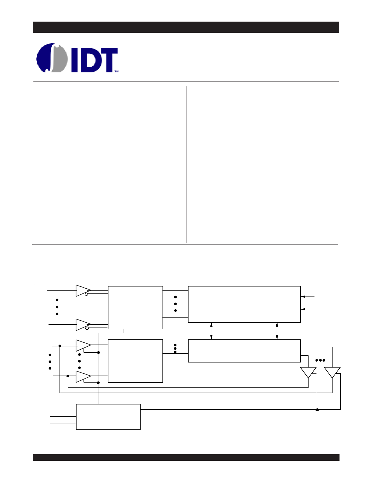
Functional Block Diagram
Description
The IDT6116SA/LA is a 16,384-bit high-speed static RAM
organized as 2K x 8. It is fabricated using IDT's high-performance,
high-reliability CMOS technology.
Access times as fast as 15ns are available. The circuit also offers a
reduced power standby mode. When CS goes HIGH, the circuit will
automatically go to, and remain in, a standby power mode, as long
as CS remains HIGH. This capability provides significant system level
power and cooling savings. The low-power (LA) version also offers a
battery backup data retention capability where the circuit typically
consumes only 1µW to 4µW operating off a 2V battery.
All inputs and outputs of the IDT6116SA/LA are TTL-compatible. Fully
static asynchronous circuitry is used, requiring no clocks or refreshing
for operation.
The IDT6116SA/LA is packaged in 24-pin 600 and 300 mil plastic or
ceramic DIP, 24-lead gull-wing SOIC, and 24-lead J-bend SOJ providing
high board-level packing densities.
Military grade product is manufactured in compliance to the latest
version of MIL-STD-883, Class B, making it ideally suited to military
temperature applications demanding the highest level of performance and
reliability.
0
A
ADDRESS
DECODER
A
10
0
/O
INPUT
DATA
CIRCUIT
I/O
7
CS
OE
WE
CONTROL
CIRCUIT
128 X 128
MEMORY
ARRAY
I/O CONTROL
MARCH 2005
CC
V
GND
3089 drw 01
1
©2005 Integrated Device Technology, Inc.
DSC-3089/05
IDT6116SA/LA
G
,
CMOS Static RAM 2K (16K x 8-Bit) Military, Commercial, and Industrial Temperature Ranges
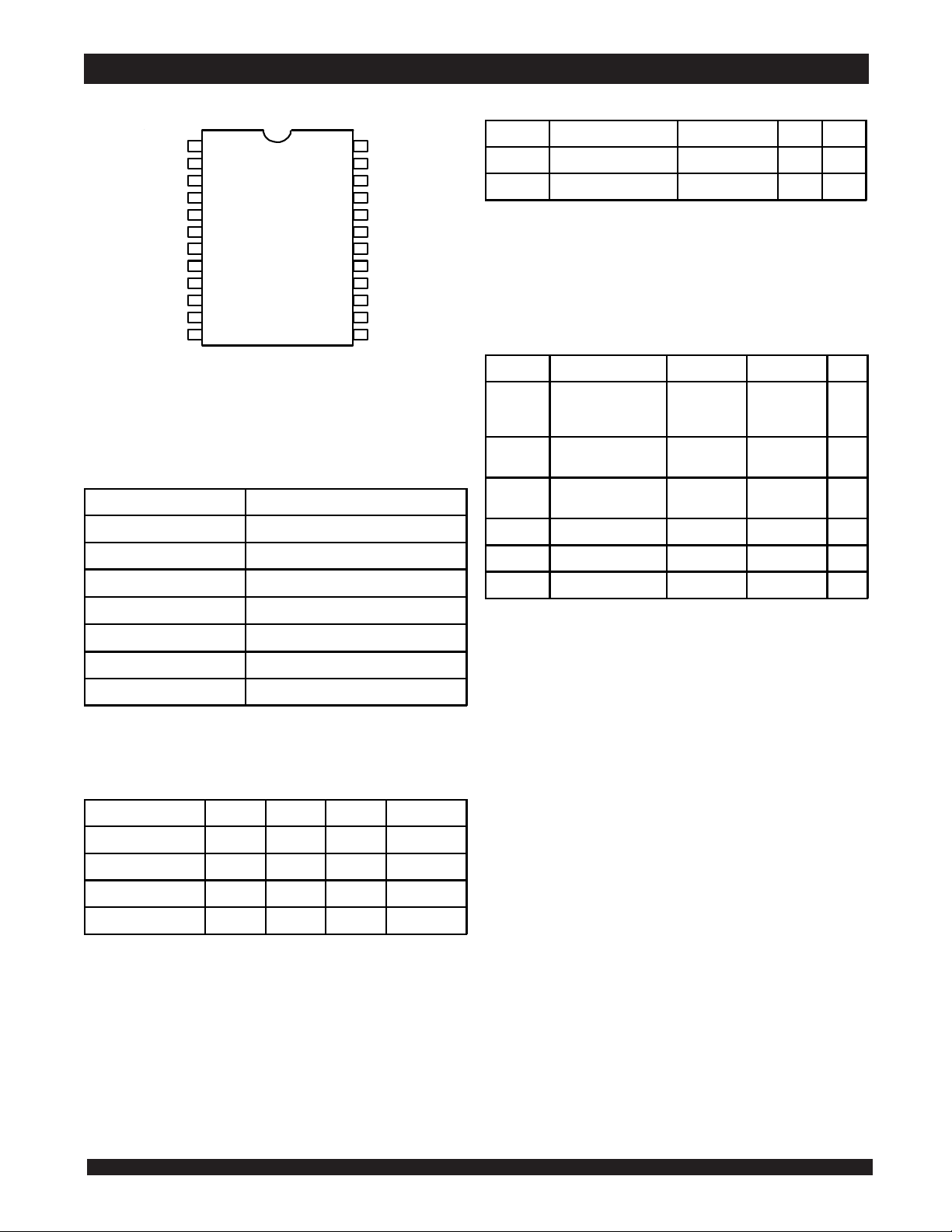
Pin Configurations
7
A
A
A
A
A
A
A
A
I/O
I/O
I/O
ND
1
6
2
5
3
4
4
3
5
2
6
1
7
0
8
0
9
1
10
2
11
P24-2
P24-1
D24-2
D24-1
SO24-2
SO24-4
12
DIP/SOIC/SOJ
Top View
Pin Description
Name Description
0
- A
10
A
0
- I/O
7
I/O
CS
WE
OE
CC
V
GND Ground
24
23
22
21
20
19
18
17
16
15
14
13
Address Inputs
Data Inp ut/ Outp ut
Chip Se le ct
Write Enable
Output Enable
V
A
A
WE
OE
A
CS
I/O
I/O
I/O
I/O
I/O
3089 drw 02
Power
CC
8
9
10
Capacitance (TA = +25°C, f = 1.0 MHZ)
Symbol Parameter
C
IN
I/O
C
NOTE:
1. This parameter is determined by device characterization, but is not production
tested.
7
6
5
4
3
3089 tbl 01
Absolute Maximum Ratings
Symbol Rating Com'l. Mil. Unit
V
TERM
A
T
T
BIAS
STG
T
P
T
OUT
I
NOTES:
1. Stresses greater than those listed under ABSOLUTE MAXIMUM RATINGS
may cause permanent damage to the device. This is a stress rating only and
functional operation of the device at these or any other conditions above those
indicated in the operational sections of this specification is not implied. Exposure
to absolute maximum rating conditions for extended periods may affect
reliability.
2. VTERM must not exceed VCC +0.5V.
Inp ut Cap ac i tance VIN = 0V 8 pF
I/O Cap ac itanc e V
(2)
Terminal Vo ltage
with Respect
to GND
Operating
Temperature
Temperature
Under Bias
Storage Temperature -55 to +125 -65 to +150oC
Po we r Dis si p atio n 1. 0 1. 0 W
DC Output Current 50 50 mA
(1)
Conditions Max. Unit
OUT
= 0V 8 pF
-0.5 to +7.0 -0.5 to +7.0 V
0 to +70 -55 to +125oC
-55 to +125 -65 to +135oC
3089 tbl 03
(1)
3 0 89 t b l 04
Truth Table
Mode
Standby H X X High-Z
Read L L H DATA
Read L H H High-Z
Write L X L DATA
NOTE:
1. H = VIH, L = VIL, X = Don't Care.
(1)
CS OE WE
I/O
OUT
IN
3 0 89 t b l 02
2
IDT6116SA/LA
CMOS Static RAM 2K (16K x 8-Bit) Military, Commercial, and Industrial Temperature Ranges
Recommended Operating
Temperature and Supply Voltage
Grade
Milita ry -55
Industrial -40
Commercial 0
Ambient
Temperature GND Vcc
O
C to + 125OC0V 5.0V ± 10%
O
C to + 85OC0V 5.0V ± 10%
O
C to +70OC0V 5.0V ± 10%
3089 tbl 05
DC Electrical Characteristics
(VCC = 5.0V ± 10%)
Symbol Parameter Test Conditions
Input Leakage Current
|I
LI
|
|I
LO
| Output Leakag e Curre nt VCC = Max., CS = VIH,
V
OL
Output Low Voltage IOL = 8mA, VCC = Min.
OH
V
Outp ut Hi g h Vol tag e IOH = -4mA, VCC = Min. 2.4
VCC = Max.,
IN =
GND to V
V
OUT
= GND to V
V
CC
CC
Recommended DC
Operating Conditions
Symbol Parameter Min. Typ. Max. Unit
V
CC
Supp ly Voltage 4.5 5.0 5.5
GND Ground 0 0 0 V
V
IH
Input High Vol tage 2.2 3.5 VCC +0.5 V
(1)
V
IL
Inp ut Low Vo ltag e -0. 5
NOTES:
1. V
IL (min.) = –3.0V for pulse width less than 20ns, once per cycle.
IN must not exceed VCC +0.5V.
2. V
____
IDT6116SA IDT6116LA
MIL.
COM'L.
MIL.
COM'L.
____
____
____
____
____
10
5
10
5
0.4
____
____
____
____
____
____
2.4
(2)
0.8 V
5
2
5
2
0.4 V
____
3089 tbl 07
V
3089 tbl 06
UnitMin. Max. Min. Max.
µA
µA
V
DC Electrical Characteristics
(1)
(VCC = 5.0V ± 10%, VLC = 0.2V, VHC = VCC - 0.2V)
6116SA15
Com'l
Symbol Parameter Power
CC1
I
I
CC2
I
SB
SB1
I
NOTES:
1. All values are maximum guaranteed values.
2. fMAX = 1/tRC, only address inputs are cycling at fMAX, f = 0 means address inputs are not changing.
Operating Power Supply Current
VIL, Outputs Ope n
CS <
V
CC
= Max., f = 0
Dynamic Operating Current
CS < V
IL
CC
= Max., f = f
V
, Outputs Ope n
MAX
(2)
Standby Po wer Supply Current
(TTL Le ve l)
VIH, Outp uts Op en
CS >
CC
= Max., f = f
V
MAX
(2)
Full Standby Power Supply Current
(CMOS Le v el )
CS > V
HC
, VCC = Max.,
IN
< VLC or VIN > VHC, f = 0
V
SA 105 105 130 80 90 80 90
LA 95 95 120 75 85 75 85
SA 150 130 150 120 135 100 115
LA 140 120 140 110 125 95 105
SA 40 40 50 40 45 25 35
LA 35 35 45 35 40 25 30
SA 2 2 10 2 10 2 10
LA 0.1 0.1 0.9 0.1 0.9 0.1 0.9
Only
6116SA20
6116LA20
Com'l
& In d
Mil
6116SA25
6116LA25
Com'l
& In d
Mil
6116SA35
6116LA35
Com'l.
& Ind. M il
Unit
mA
mA
mA
mA
3089 tbl 08
6.42
3
IDT6116SA/LA
CMOS Static RAM 2K (16K x 8-Bit) Military, Commercial, and Industrial Temperature Ranges
(1)
DC Electrical Characteristics
(continued)
(VCC = 5.0V ± 10%, VLC = 0.2V, VHC = VCC - 0.2V)
6116SA45
6116LA45
Com'l
Symbol Parameter Power
CC1
Operating Power Supply
I
Current , CS <
VIL,
Outputs Open
CC
= Max., f = 0
V
CC2
Dynamic Operating
I
Current , CS <
Outputs Open
CC
= Max., f = f
V
SB
Standby Power Supply
I
VIL,
MAX
(2)
Curren t (TTL Lev el)
VIH, Outp uts Op en
CS >
V
SB1
Full Standby Power
I
CC
= Max., f = f
MAX
(2)
Supply Current (CMOS
Level), CS >
CC
V
VHC,
= Max., VIN < V
LC
or VIN > VHC, f = 0
NOTES:
1. All values are maximum guaranteed values.
2. fMAX = 1/tRC, only address inputs are toggling at fMAX, f = 0 means address inputs are not changing.
& Ind
SA 80 90 90 90 90 90 90
LA 75 85 85 85 85 85 85
SA 100 100 100 100 100 100 90
LA 90 95 90 90 85 85 85
SA 25 25 25 25 25 25 25
LA 20 20 20 20 25 15 15
SA 2 10 10 10 10 10 10
LA 0.1 0.9 0.9 0.9 0.9 0.9 0.9
6116SA55
6116LA55
6116SA70
6116LA70
6116SA90
6116LA90
6116SA120
6116LA120
6116SA150
6116LA150
Mil Mil Only Mil Only Mil Only Mil Only Mil Only
3089 tbl 09
Unit
mA
mA
mA
mA
Data Retention Characteristics Over All Temperature Ranges
(LA Version Only) (VLC = 0.2V, VHC = VCC – 0.2V)
(1)
Typ.
VCC @
Symbol Parameter Test Condition M in. 2.0V 3. 0V 2.0V 3.0V Unit
V
I
CCDR
DR
VCC fo r Da ta R e tent i o n
Data Re te ntio n Cu rre nt MIL.
____
COM'L.
(3)
t
CDR
Chip De s e le c t to Data
Retention Time
(3)
R
t
I
I
LI
I
NOTES:
1. TA = + 25°C
2. tRC = Read Cycle Time.
3. This parameter is guaranteed by device characterization, but is not production tested.
Op e ration Re c o ve ry Tim e
Input Leakag e Current
V
HC
CS >
VIN > VHC or < V
LC
2.0
____
____
____
(2)
RC
t
____ ____ ____
____ ____ ____ ____
0.5
0.5
0
____ ____ ____ ____
1.5
1.5
____ ____ ____
Max.
V
CC
@
200
20
300
30
22
V
µA
ns
ns
µA
3089 tbl 10
4

IDT6116SA/LA
V
,
D
,
D
,
CMOS Static RAM 2K (16K x 8-Bit) Military, Commercial, and Industrial Temperature Ranges
Low VCC Data Retention Waveform
DATA RETENTION MODE
CC
CS
t
CDR
V
4.5V
IH
DR
≥ 2V
V
DR
V
4.5V
R
t
V
IH
3089 drw 03
AC Test Conditions
Input Pulse Levels
Input Rise/Fall Times
Input Timing Refere nce Lev el s
Output Refere nce Le vel s
AC Test Load
GND to 3. 0V
5ns
1.5V
1.5V
See Figures 1 and 2
3089 tbl 11
ATA
OUT
255Ω
Figure 1. AC Test Load
5V
480Ω
30pF*
3089 drw 04
ATA
*Including scope and jig.
OUT
255Ω
Figure 2. AC Test Load
(for tOLZ, tCLZ, tOHZ, tWHZ, tCHZ & tOW)
5V
480Ω
5pF*
3089 drw 05
6.42
5

IDT6116SA/LA
CMOS Static RAM 2K (16K x 8-Bit) Military, Commercial, and Industrial Temperature Ranges
AC Electrical Characteristics (VCC = 5V ± 10%, All Temperature Ranges)
(1)
6116SA15
6116SA20
6116LA20
6116SA25
6116LA25
6116SA35
6116LA35
Symbol Parameter
Min. Max. Min. Max. Min. Max. Min. Max.
Unit
Read Cycl e
t
RC
t
AA
t
ACS
t
CLZ
t
OE
t
OLZ
t
CHZ
t
OHZ
t
OH
t
PU
t
PD
Rea d Cy c le Time 15
Address Access Time
Chip Select Access Time
(3)
Chip Select to Output in Low-Z 5
Outp u t En ab l e to O utp u t Vali d
(3)
Output Enab le to Output in Lo w-Z 0
(3)
Chip De s ele c t to Output in Hi g h-Z
(3)
Outp u t Dis a b le to Outp u t in H ig h -Z
Output Hold from Ad dre ss Change 5
(3)
Chip Se l ec t to Po we r Up Time 0
(3)
Chip Deselect to Power Down Time
____
____
15
____
15
____
____
10
____
____
10
____
8
____
____
____
15
____
20
____
19
____
20
____
5
____
10
____
0
____
11
____
8
____
5
____
0
____
20
____
____
____
____
____
____
____
25
25
25
____
5
13
____
5
12
10
____
5
____
0
25
____
35
____
____
5
____
5
____
____
5
0
____
35 ns
35 ns
____
20 ns
____
15 ns
13 ns
____
____
35 ns
30 89 tb l 12
ns
ns
ns
ns
ns
AC Electrical Characteristics (VCC = 5V ± 10%, All Temperature Ranges) (continued)
Symbol Parameter
6116SA45
6116LA45
6116SA55
6116LA55
(2)
6116SA70
(2)
6116LA70
Min. Max. Min. Max. Min. Max. Min. Max. Min. Max. Min. Max.
(2)
6116SA90
(2)
6116LA90
(2)
(2)
6116SA120
6116LA120
(2)
(2)
6116SA150
6116LA150
(2)
(2)
Unit
Read Cycl e
t
RC
t
AA
t
ACS
t
CLZ
OE
t
t
OLZ
CHZ
t
OHZ
t
OH
t
Read Cy cle Time 45
Address Access Time
Chip Select Access Time
(3)
Chip Select to Output in Low-Z 5
Outp u t En ab l e to O utp u t Vali d
(3)
Output Enab le to Output in Lo w-Z 5
(3)
Chip De s ele c t to Output in Hi g h-Z
(3)
Outp u t Dis a b le to Outp u t in H ig h -Z
Output Hold from Ad dre ss Change 5
____
____
45
____
45
____
____
25
____
____
20
____
15
____
NOTES:
1. 0°C to +70°C temperature range only.
2. –55°C to +125°C temperature range only.
3. This parameter guaranteed with the AC Load (Figure 2) by device characterization, but is not production tested.
____
55
____
55
____
50
____
5
____
40
____
5
____
30
____
30
____
5
____
70
____
____
5
____
5
____
____
5
____
____
____
90
____
70
____
65
5
____
50
5
____
35
____
35
5
____
90
90
____
60
____
40
40
____
120
____
____
____
____
____
____
120
120
____
5
80
____
5
40
40
____
5
150
____
____
____
____
____
5
5
5
____
150 ns
150 ns
____
100 ns
____
40 ns
40 ns
____
30 89 tb l 13
ns
ns
ns
ns
6

IDT6116SA/LA
V
S
C
,
A
,
D
,
CMOS Static RAM 2K (16K x 8-Bit) Military, Commercial, and Industrial Temperature Ranges
Timing Waveform of Read Cycle No. 1
t
RC
(1,3)
ADDRESS
t
AA
t
OH
OE
t
OE
CC
DATA
CS
OUT
I
CC
t
ACS
(5)
t
CLZ
t
PU
t
OLZ
(5)
upply
urrents
I
SB
Timing Waveform of Read Cycle No. 2
RC
t
DDRESS
t
AA
DATA
OUT
PREVIOUS DATA VALID
t
OH
(1,2,4)
(5)
t
OHZ
(5)
t
CHZ
DATA
VALID
DATAVALID
t
PD
3089 drw 06
t
OH
3089drw07
Timing Waveform of Read Cycle No. 3
(1,3,4)
CS
ACS
t
(5)
t
CLZ
ATA
OUT
NOTES:
1. WE is HIGH for Read cycle.
2. Device is continously selected, CS is LOW.
3. Address valid prior to or coincident with CS transition LOW.
4. OE is LOW.
5. Transition is measured ±500mV from steady state.
6.42
7
DATA VALID
t
CHZ
(5)
3089 drw 08

IDT6116SA/LA
CMOS Static RAM 2K (16K x 8-Bit) Military, Commercial, and Industrial Temperature Ranges
AC Electrical Characteristics (VCC = 5V ± 10%, All Temperature Ranges)
(1)
6116SA15
6116SA20
6116LA20
Symbol Parameter Min. Max. Min. Max. Min. Max. Min. Max. Unit
Write Cycle
____
____
20
____
15
____
15
____
0
____
12
____
0
____
7
____
12
____
0
____
0
t
WC
t
CW
AW
t
t
AS
t
WP
WR
t
t
WHZ
DW
t
DH
t
OW
t
Write Cycle Time 15
Chip Select to End-of-Write 13
Address Valid to End-of-Write 14
Address Set-up Time 0
Write Pulse Width 12
Write Reco v e ry Time 0
(3)
Write to Output in Hig h-Z
Data to Write Time Overlap 12
(4)
Data Ho ld fro m Writ e Tim e 0
(3,4)
Output A cti v e from End - o f- Wr it e 0
6116SA25
6116LA25
____
25
____
17
____
17
____
0
____
15
____
0
____
8
____
13
____
0
____
0
6116SA35
6116LA35
____
____
____
____
____
____
16
____
____
____
____
____
35
____
25
____
25
____
0
____
20
____
0
20 ns
____
15
____
0
____
0
ns
ns
ns
ns
ns
ns
ns
ns
ns
3089 tbl 14
AC Electrical Characteristics (VCC = 5V ± 10%, All Temperature Ranges) (continued)
(2)
6116SA45
6116LA45
6116SA55
6116LA55
6116SA70
(2)
Symbol Parameter Min. Max. Min. Max. Min. Max. Min. Max. Min. Max. Min. Max. Unit
Write Cycle
____
____
____
____
____
____
____
25
____
____
____
t
WC
CW
t
AW
t
AS
t
WP
t
WR
t
t
WHZ
t
DW
t
DH
OW
t
Write Cycle Time 45
Chip Select to End-of-Write 30
Address Valid to End-of-Write 30
Address Set-up Time 0
Write Pulse Width 25
Write Reco v e ry Time 0
(3)
Write to Output in Hig h-Z
Data to Write Time Overlap 20
(4)
Data Ho ld fro m Writ e Tim e 0
(3,4)
Output A cti v e from End - o f- Wri t e 0
NOTES:
1. 0°C to +70°C temperature range only.
2. –55°C to +125°C temperature range only.
3. This parameter guaranteed with AC Load (Figure 2) by device characterization, but is not production tested.
4. The specification for tDH must be met by the device supplying write data to the RAM under all operation conditions. Although tDH and tOW values will vary over voltage
and temperature, the actual tDH will always be smaller than the actual tOW.
55
40
45
40
____
25
____
____
____
____
5
____
____
5
30
____
____
5
____
0
6116LA70
70
40
65
15
40
5
____
30
5
0
(2)
6116SA90
(2)
6116LA90
____
____
____
____
____
____
____
35
____
____
____
(2)
6116SA120
(2)
6116LA120
____
90
55
80
15
55
5
30
5
0
120
____
70
____
105
____
20
____
70
____
____
40
____
35
____
____
(2)
6116SA150
(2)
6116LA150
____
150
____
90
____
120
____
20
____
90
____
5
5
0
10
____
40
____
40
____
10
____
(2)
(2)
____
ns
____
ns
____
ns
____
ns
____
ns
____
ns
40 ns
____
ns
____
ns
____
0
ns
30 89 tb l 15
8

IDT6116SA/LA
A
,
t
A
,
CMOS Static RAM 2K (16K x 8-Bit) Military, Commercial, and Industrial Temperature Ranges
Timing Waveform of Write Cycle No. 1 (WE Controlled Timing)
t
WC
(1,2,5,7)
DDRESS
t
AW
CS
t
AS
(7)
t
WP
(3)
t
WR
t
CHZ
(6)
WE
(6)
t
DATA
DATA
OUT
WHZ
PREVIOUS DATA VALID
IN
(4)
t
DW
DATA VALID
(6)
t
OW
DATA
(4)
VALID
t
DH
3089 drw 09
Timing Waveform of Write Cycle No. 2 (CS Controlled Timing)
WC
(1,2,3,5,7)
DDRESS
t
AW
CS
t
AS
t
CW
t
WR
(3)
WE
t
DW
DATA
IN
NOTES:
1. WE or CS must be HIGH during all address transitions.
2. A write occurs during the overlap of a LOW CS and a LOW WE.
3. tWR is measured from the earlier of CS or WE going HIGH to the end of the write cycle.
4. During this period, the I/O pins are in the output state and the input signals must not be applied.
5. If the CS LOW transition occurs simultaneously with or after the WE LOW transition, the outputs remain in the high-impedance state.
6. Transition is measured ±500mV from steady state.
7. OE is continuously HIGH. If OE is LOW during a WE controlled write cycle, the write pulse width must be the larger of tWP or (tWHZ + tDW) to allow the I/O drivers
to turn off and data to be placed on the bus for the required tDW. If OE is HIGH during a WE controlled write cycle, this requirement does not apply and the write pulse
is the specified tWP. For a CS controlled write cycle, OE may be LOW with no degradation to tCW.
DATA VALID
t
DH
3089drw 10
6.42
9

IDT6116SA/LA
I
,
I
,
CMOS Static RAM 2K (16K x 8-Bit) Military, Commercial, and Industrial Temperature Ranges
Ordering Information — Military
DT 6116
Device TypeXXPower
XXX
SpeedXPackageXProcess/
Temperature
Range
B
TD
D
20*
25*
35*
45
55
70
90
120
150**
SA
LA
Military (-55°C to +125°C)
Compliant to MIL-STD-883,ClassB
300 mil CERDIP(D 24-1)
600 mil CERDIP(D 24-2)
Speed in nanoseconds
Standard Power
Low Power
*Available in 300 mil packaging only.
**Available in 600 mil packaging only.
3089 drw 11
Ordering Information — Commercial & Industrial
DT 6116
Device TypeXXPower
XXX
SpeedXPackage
X
X
Process/
Temperature
Range
Commercial (0°C to +70°C)
Blank
Industrial (-40°Cto +85°C)
I
G Restricted hazardous substance device
TP
P
SO
Y
15*
20
25
35
45
SA
LA
*Available in commercial temperature range and standard poweronly.
300 mil PlasticD IP (P24-1)
600 mil PlasticD IP (P24-2)
300 mil Small Outline IC, Gull-Wing Bend (SO24-2)
300 mil SOJ, J-Bend(SO24-4)
Speed in nanoseconds
Standard Power
Low Power
10
3089 drw 12

IDT6116SA/LA
CMOS Static RAM 2K (16K x 8-Bit) Military, Commercial, and Industrial Temperature Ranges
Datasheet Document History
1/7/00 Updated to new format
Pg. 1, 3, 4, 10 Added Industrial Temperature range offerings
Pg. 9, 10 Separated ordering information into military, commercial, and industrial temperature range offerings
Pg. 11 Added Datasheet Document History
08/09/00 Not recommended for new designs
02/01/01 Removed "Not recommended for new designs"
12/30/03 Pg. 3,10 Corrected Industrial temp from -45C to -40C.
03/31/05 Pg. 10 Added "Restricted hazardous substance device" to ordering information.
CORPORATE HEADQUARTERS for SALES: for Tech Support:
6024 Silver Creek Valley Road 800-345-7015 or ipchelp@idt.com
San Jose, CA 95138 408-284-8200 800-345-7015
fax: 408-284-2775
www.idt.com
The IDT logo is a registered trademark of Integrated Device Technology, Inc.
6.42
11
 Loading...