

Datasheet IDT54FCT162511ATPV, IDT54FCT162511ATPVB, IDT54FCT162511CTE, IDT54FCT162511CTEB, IDT54FCT162511CTPAB Datasheet (Integrated Device Technology Inc)
...Page 1
Integrated Device Technology, Inc.
FAST CMOS 16-BIT
REGISTERED/LATCHED
TRANSCEIVER WITH PARITY
IDT54/74FCT162511AT/CT
FEATURES:
• 0.5 MICRON CMOS Technology
• Typical tsk(o) (Output Skew) < 250ps, clocked mode
• Low input and output leakage ≤1µA (max)
• ESD > 2000V per MIL-STD-883, Method 3015;
> 200V using machine model (C = 200pF, R = 0)
• Packages include 25 mil pitch SSOP, 19.6 mil pitch TSSOP,
15.7 mil pitch TVSOP and 25 mil pitch Cerpack
• Extended commercial range of –40°C to +85°C
•VCC = 5V ±10%
• Balanced Output Drivers: ±24mA (commercial)
±16mA (military)
• Series current limiting resistors
• Generate/Check, Check/Check modes
• Open drain parity error allows wire-OR
DESCRIPTION:
The FCT162511AT/CT 16-bit registered/latched transceiver
with parity is built using advanced dual metal CMOS technology. This high-speed, low-power transceiver combines D-
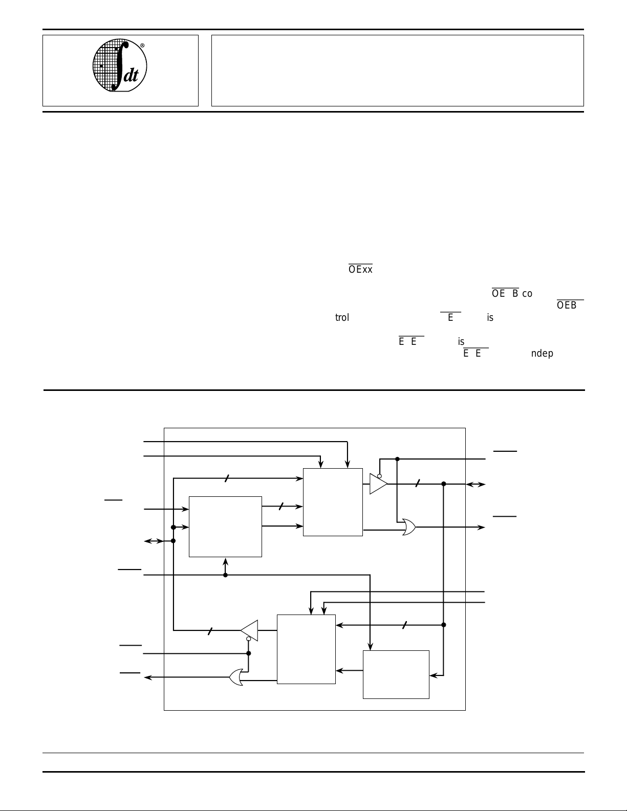
SIMPLIFIED FUNCTIONAL BLOCK DIAGRAM:
type latches and D-type flip-flops to allow data flow in transparent, latched or clocked modes. The device has a parity
generator/cheker in the A-to-B direction and a parity checker
in the B-to-A direction. Error checking is done at the byte level
with separate parity bits for each byte. Separate error flags
exits for each direction with a single error flag indicating an
error for either byte in the A-to-B direction and a second error
flag indicating an error for either byte in the B-to-A direction.
The parity error flags are open drain outputs which can be tied
together and/or tied with flags from other devices to form a
single error flag or interrupt. The parity error flags are enabled
by the
OExx
control pins allowing the designer to disable the
error flag during combinational transitions.
The control pins LEAB, CLKAB and
tion in the A-to-B direction while LEBA, CLKBA and
control the B-to-A direction.
GEN
/CHK is only for the selection
OEAB
control opera-
OEBA
of A-to-B operation, the B-to-A direction is always in checking
mode. The ODD/
directions. Except for the ODD/
EVEN
select is common between the two
EVEN
control, independent
operation can be achieved between the two directions by
using the corresponding control lines.
LEAB
CLKAB
GEN/CHK
A0-15
PA1,2
ODD/EVEN
OEBA
PERA
(Open Drain)
Data
Byte
Parity
Generator/
Checker
Parity, data
18
16
Parity
2
Latch/
Register
Latch/
Register
Parity, data
Parity, Data
18
Byte
Parity
Checking
18
OEAB
B0-15
PB1,2
PERB
(Open Drain)
LEBA
CLKBA
2916 drw 01
The IDT logo is a registered trademark of Integrated Device Technology, Inc.
MILITARY AND COMMERCIAL TEMPERATURE RANGES AUGUST 1996
1996 Integrated Device Technology, Inc. 5.11 DSC–2916/5
1
Page 2

IDT54/74FCT162511AT/CT
FAST CMOS 16-BIT REGISTERED/LATCHED TRANSCEIVER WITH PARITY MILITARY AND COMMERCIAL TEMPERATURE RANGES
FUNCTIONAL BLOCK DIAGRAM
ODD/EVEN
OEAB
LEBA
CLKBA
CLKAB
LEAB
A0 - A
OEBA
PA
A8 - A
C
7
D
C
D
C
D
B0 - B
7
C
D
P
1
O
C
D
I
C
D
C
PB
1
D
P
C
D
C
15
D
C
D
C
D
B8 - B
15
C
D
PA
2
GEN/CHK
PERA
(Open Drain)
P
O
C
D
I
C
D
PB
2
C
D
C
D
C
D
5.11 2
C
D
C
D
PERB
(Open Drain)
C
D
P
2916 drw 02
Page 3
IDT54/74FCT162511AT/CT
FAST CMOS 16-BIT REGISTERED/LATCHED TRANSCEIVER WITH PARITY MILITARY AND COMMERCIAL TEMPERATURE RANGES
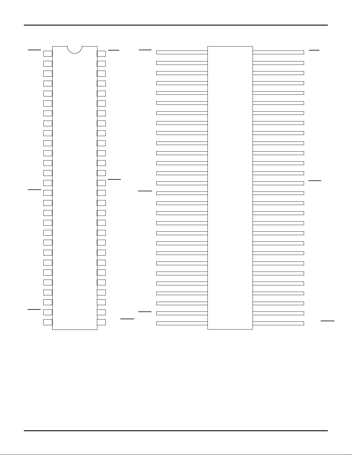
PIN CONFIGURATIONS
OEAB
LEAB
PA
GND
A
A
V
CC
A
A
A
A
A
A
GND
PERA
A
A
A
A
A
A
V
CC
A
A
GND
PA
OEBA
LEBA
1
2
1
3
4
0
1
5
6
7
2
3
4
5
6
7
8
9
10
11
12
13
8
9
10
11
12
13
14
15
16
17
18
19
20
21
SO56-1
SO56-2
SO56-3
22
14
15
2
23
24
26
27
28
56
55
54
53
52
51
50
49
48
47
46
45
44
43
42
41
40
39
38
37
36
35
34
33
3225
31
30
29
GEN/CHK
CLKAB
PB
1
GND
0
B
B
1
V
CC
2
B
B
3
B
4
B
5
B
6
B
7
PERB
GND
B
8
B
9
B
10
B
11
B
12
B
13
V
CC
14
B
B
15
GND
2
PB
CLKBA
ODD/EVEN
OEAB
LEAB
PA
GND
A
A1
VCC
A2
A3
A4
A5
A6
A7
GND
PERA
A
A9
A
A11
A12
A
VCC
A14
A
GND
PA2
OEBA
LEBA
1
0
8
10
13
15
1
2
3
4
5
6
7
8
9
10
11
12
13
14
15
16
17
18
19
20
21
22
23
24
26
27
28
E56-1
56
55
54
53
52
51
50
49
48
47
46
45
44
43
42
41
40
39
38
37
36
35
34
33
3225
31
30
29
GEN/CHK
CLKAB
PB1
GND
B
0
B1
VCC
2
B
B3
B4
B5
B6
B7
PERB
GND
8
B
B9
B10
B11
B12
B13
VCC
B
14
B15
GND
PB
2
CLKBA
ODD/EVEN
SSOP/
TSSOP/TVSOP
TOP VIEW
2916 drw 03
CERPACK
TOP VIEW
2916 drw 04
5.11 3
Page 4
IDT54/74FCT162511AT/CT
FAST CMOS 16-BIT REGISTERED/LATCHED TRANSCEIVER WITH PARITY MILITARY AND COMMERCIAL TEMPERATURE RANGES
ABSOLUTE MAXIMUM RATINGS
(1)
Symbol Description Max. Unit
(2)
VTERM
VTERM
Terminal Voltage with Respect to
GND
(3)
Terminal Voltage with Respect to
GND
–0.5 to +7.0 V
–0.5 to
CC +0.5
V
V
TSTG Storage Temperature –65 to +150 °C
IOUT DC Output Current –60 to +120 mA
NOTES:
1. Stresses greater than those listed under ABSOLUTE MAXIMUM RATINGS may cause permanent damage to the device. This is a stress rating
only and functional operation of the device at these or any other conditions
above those indicated in the operational sections of this specification is
not implied. Exposure to absolute maximum rating conditions for
extended periods may affect reliability.
2. Open drain and all device terminals except FCT162XXXT Output and I/O
terminals.
3. Output and I/O terminals for FCT162XXXT.
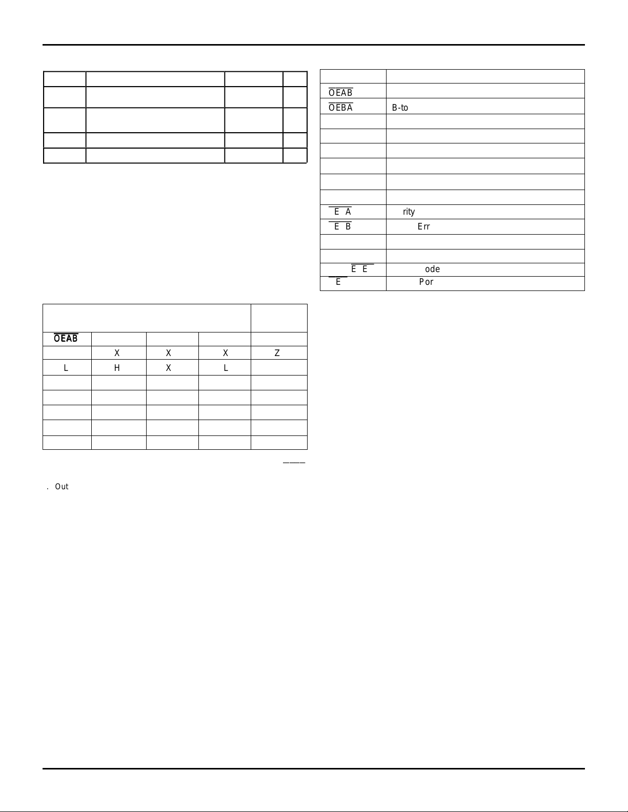
FUNCTION TABLE
(1,4)
2916 lnk 01
Inputs Outputs
OEAB
OEAB
LEAB CLKAB Ax Bx
HXX XZ
LHX LL
LHX HH
LL↑ LL
LL↑ HH
LLL XB
LLH XB
NOTES: 2916 tbl 02
1. A-to-B data flow is shown. B-to-A data flow is similar but uses
LEBA, and CLKBA.
2. Output level before the indicated steady-state input conditions were
established.
3. Output level before the indicated steady-state input conditions were
established, provided that CLKAB was HIGH before LEAB went LOW.
4. H = HIGH Voltage Level
L = LOW Voltage Level
X = Don't Care
Z = High Impedance
↑ = LOW-to-HIGH Transition
(2)
(3)
OEBA
PIN DESCRIPTION
Pin Names Description
OEAB
OEBA
LEAB A-to-B Latch Enable Input
LEBA B-to-A Latch Enable Input
CLKAB A-to-B Clock Input
CLKBA B-to-A Clock Input
Ax A-to-B Data Inputs or B-to-A 3-State Outputs
Bx B-to-A Data Inputs or A-to-B 3-State Outputs
PERA
PERB
(1)
PAx
PBx B-to-A Parity Input, A-to-B Parity Output
ODD/
EVEN
GEN
/CHK A to B Port Generate or Check Mode Input
NOTES:
1. The PAx pin input is internally disabled during parity generation. This
means that when generating parity in the A to B direction there is no need
to add a pull up resistor to guarantee state. The pin will still function
properly as the parity output for the B to A direction.
,
A-to-B Output Enable Input (Active LOW)
B-to-A Output Enable Input (Active LOW)
Parity Error (Open Drain) on A Outputs
Parity Error (Open Drain) on B Outputs
A-to-B Parity Input, B-to-A Parity Output
Parity Mode Selection Input
2916 tbl 03
5.11 4
Page 5

IDT54/74FCT162511AT/CT
FAST CMOS 16-BIT REGISTERED/LATCHED TRANSCEIVER WITH PARITY MILITARY AND COMMERCIAL TEMPERATURE RANGES
CAPACITANCE (TA = +25°C, f = 1.0MHz)
Symbol Parameter
CIN Input
Capacitance
CI/O I/O
Capacitance
CO Open Drain
Capacitance
NOTE:
1. This parameter is measured at characterization but not tested.
(1)
Conditions Typ. Max. Unit
VIN = 0V 3.5 6.0 pF
VOUT = 0V 3.5 8.0 pF
VOUT = 0V 3.5 6.0 pF
2916 lnk 04
FUNCTION TABLE
(PARITY CHECKING)
A0 - A7 and PA1
of inputs that are high
NOTES:
1. Conditions shown are for
2. A-to-B parity checking is shown. B-to-A parity checking is similar but uses
OEBA
3. In parity checking mode the parity bits will be transmitted unchanged along
4. The response shown is for LEAB = H. If LEAB = L then CLKAB will control
5. Conditions shown are for the byte A
6. The parity error flag
= L,
with the corresponding data regardless of parity errors. (PB1 = PA1).
as an edge triggered clock.
2 is similiar.
PA
15. If a parity error occurs on either byte
A
open drain output which must be externally pulled up to achieve a logic
HIGH.
(5)
, Total Number
1, 3, 5, 7 or 9 L L
1, 3, 5, 7 or 9 H H
0, 2, 4, 6 or 8 L H
0, 2, 4, 6 or 8 H L
OEAB
= H and errors will be indicated on
PERB
(1, 2, 3, 4)
ODD/
EVEN
EVEN
GEN
/CHK = H,
is a combined flag for both bytes A
OEAB
= L,
OEBA
PERA
0-A7 and PA1. The byte A8-A15 and
PERB
will go low.
PERB
PERB
(6)
(6)
2916 tbl 05
= H.
.
0-A7 and A8-
PERB
is an
FUNCTION TABLE
(PARITY GENERATION)
A0 - A7, Total Number
of inputs that are high
1, 3, 5 or 7 L H
1, 3, 5 or 7 H L
0, 2, 4, 6 or 8 L L
0, 2, 4, 6 or 8 H H
NOTES:
1. Conditions shown are for
2. A-to-B parity checking is shown. B-to-A is capable of parity checking while
A-to-B is performing generation. B-to-A will not generate parity.
3. The response shown is for LEAB = H. If LEAB = L then CLKAB will control
as an edge triggered clock.
4. Conditions shown are for the byte A
will output the parity on PB
5. The error flag
PERB
GEN
will remain in a high state during parity generation.
(1, 2, 3, 4, 5)
ODD/
EVEN
EVEN
/CHK = L,
2.
OEAB
= L,
OEBA
0-A7 . The byte A8-A15 is similiar but
PB
= H.
1
2916 tbl 06
5.11 5
Page 6

IDT54/74FCT162511AT/CT
FAST CMOS 16-BIT REGISTERED/LATCHED TRANSCEIVER WITH PARITY MILITARY AND COMMERCIAL TEMPERATURE RANGES
DC ELECTRICAL CHARACTERISTICS OVER OPERATING RANGE
Following Conditions Apply Unless Otherwise Specified:
Commercial: TA = –40°C to +85°C, VCC = 5.0V ± 10%; Military: TA = –55°C to +125°C, VCC = 5.0V ± 10%
Symbol Parameter Test Conditions
(1)
Min. Typ.
VIH Input HIGH Level Guaranteed Logic HIGH Level 2.0 — — V
VIL Input LOW Level Guaranteed Logic LOW Level — — 0.8 V
II H Input HIGH Current (Input pins)
Input HIGH Current (I/O pins)
II L Input LOW Current (Input pins)
Input LOW Current (I/O pins)
(5)
VCC = Max. VI = VCC — — ±1 µA
(5)
(5)
VI = GND — — ±1
(5)
— — ±1
— — ±1
IOZH High Impedance Output Current VCC = Max. VO = 2.7V — — ±1 µA
IOZL (3-State Output pins)
(5)
VO = 0.5V — — ±1
VIK Clamp Diode Voltage VCC = Min., IIN = –18mA — –0.7 –1.2 V
IOS Short Circuit Current VCC = Max., VO = GND
(3)
–80 –140 –225 mA
VH Input Hysteresis — — 100 — mV
ICCL
Quiescent Power Supply Current VCC = Max., VIN = GND or VCC — 5 500 µA
ICCH
ICCZ
(2)
Max. Unit
2916 lnk 07
OUTPUT DRIVE CHARACTERISTICS FOR FCT162511T
Symbol Parameter Test Conditions
IODL Output LOW (I/O pins) VCC = 5V, VIN = VIH or VIL, VOUT = 1.5V
(1)
(3)
Min. Typ.
60 115 200 mA
Current (Open Drain) — 250 — mA
IODH Output HIGH Current (I/O pins) VCC = 5V, VIN = VIH or VIL, VOUT = 1.5V
IOFF Output Power Off Leakage
Current (Open Drain)
(5)
VOH Output HIGH Voltage (I/O pins) VCC = Min.
VOL Output LOW
(I/O pins) VCC = Min.
Voltage
VCC = 0, VO ≤ 5.5V ——±1µA
IOH = –16mA MIL.
V
IN = VIH or VIL
I
OH = –24mA COM'L.
IOL = 16mA MIL.
V
IN = VIH or VIL
I
OL = 24mA COM'L.
(Open Drain) IOL = 48mA MIL.
I
OL = 64mA COM'L.
NOTES:
1. For conditions shown as Max. or Min., use appropriate value specified under Electrical Characteristics for the applicable device type.
2. Typical values are at Vcc = 5.0V, +25°C ambient.
3. Not more than one output should be tested at one time. Duration of the test should not exceed one second.
4. Duration of the condition can not exceed one second.
5. The test limit for this parameter is ± 5µA at T
A = –55°C.
(3)
–60 –115 –200 mA
2.4 3.3 —
— 0.3 0.55
— 0.3 0.55
(2)
Max. Unit
V
V
V
2916 tbl 08
5.11 6
Page 7

IDT54/74FCT162511AT/CT
FAST CMOS 16-BIT REGISTERED/LATCHED TRANSCEIVER WITH PARITY MILITARY AND COMMERCIAL TEMPERATURE RANGES
POWER SUPPLY CHARACTERISTICS
Symbol Parameter Test Conditions
CC Quiescent Power Supply VCC = Max. All other Input Pins — 0.5 1.5 mA
∆I
Current TTL Inputs HIGH V
I
CCD Dynamic Power Supply Current
IN = 3.4V
(4)
VCC = Max., Outputs Open VIN = VCC — 75 120 µA/
OEAB
(3)
= GND,
Parity Input Pins (PAx, PBx) — 1.0 2.5
OEBA
(1)
= V
CC VIN = GND MHz
Min. Typ.
One Input Toggling
50% Duty Cycle
I
C Total Power Supply Current
(6)
VCC = Max., Outputs Open VIN = VCC — 0.8 1.7 mA
f
CP = 10MHz (CLKAB) VIN = GND
50% Duty Cycle
OEAB
= GND,
OEBA
= V
CC
LEAB = GND VIN = 3.4V — 1.3 3.2
One Bit Toggling V
f
i = 5MHz
IN = GND
50% Duty Cycle
V
CC = Max., Outputs Open VIN = VCC — 3.8 6.5
fCP = 10MHz (CLKAB) VIN = GND
50% Duty Cycle
OEAB
= GND,
OEBA
= V
CC
LEAB = GND VIN = 3.4V — 9.0 21.8
Eighteen Bits Toggling VIN = GND
f
i = 2.5MHz
50% Duty Cycle
NOTES:
1. For conditions shown as Max. or Min., use appropriate value specified under Electrical Characteristics for the applicable device type.
2. Typical values are at V
3. Per TTL driven input (V
4. This parameter is not directly testable, but is derived for use in Total Power Supply Calculations.
5. Values for these conditions are examples of the I
C = IQUIESCENT + IINPUTS + IDYNAMIC
6. I
IC = ICC + ∆ICC DHNT + ICCD (fCPNCP/2 + fiNi)
I
CC = Quiescent Current (ICCL, ICCH and ICCZ)
CC = Power Supply Current for a TTL High Input (VIN = 3.4V)
∆I
D
H = Duty Cycle for TTL Inputs High
T = Number of TTL Inputs at DH
N
ICCD = Dynamic Current Caused by an Input Transition Pair (HLH or LHL)
CP = Clock Frequency for Register Devices (Zero for Non-Register Devices)
f
N
CP = Number of Clock Inputs at fCP
fi = Input Frequency
i = Number of Inputs at fi
N
CC = 5.0V, +25°C ambient.
IN = 3.4V). All other inputs at VCC or GND.
CC formula. These limits are guaranteed but not tested.
(2)
Max. Unit
(5)
(5)
2916 tbl 09
5.11 7
Page 8

IDT54/74FCT162511AT/CT
FAST CMOS 16-BIT REGISTERED/LATCHED TRANSCEIVER WITH PARITY MILITARY AND COMMERCIAL TEMPERATURE RANGES
SWITCHING CHARACTERISTICS OVER OPERATING RANGE (PROPAGATION DELAYS)
FCT162511AT FCT162511CT
Com'l. Mil. Com'l. Mil.
Symbol Parameter Condition
tPLH
tPHL
tPLH Propagation Delay
Propagation Delay, PAx to PBx
Ax to Bx or Bx to Ax, PBx to PAx
GEN
/CHK LOW 1.5 7.5 1.5 8.0 1.5 6.5 1.5 6.8 ns
CL = 50pF
R
(1)
L = 500Ω
tPHL Ax to PBx
(3)
tPLH
tPHL Ax to
tPLH
tPHL Bx to
tPLH
tPHL
Propagation Delay 1.5 9.0 1.5 9.0 1.5 7.5 1.5 7.8 ns
PERB
, PAx to
(3)
Propagation Delay 1.5 9.0 1.5 9.0 1.5 7.5 1.5 7.8 ns
PERA
, PBx to
PERB
PERA
Propagation Delay
LEBA to Ax and PAx
LEAB to Bx and PBx
(3)
tPLH
tPHL LEBA to
tPLH
tPHL
Propagation Delay 1.5 7.0 1.5 7.0 1.5 6.0 1.5 6.3 ns
PERA
, LEAB to
PERB
1.5 6.0 1.5 6.0 1.5 5.0 1.5 5.3
Propagation Delay
CLKBA to Ax and PAx
CLKAB to Bx and PBx
(3)
tPLH
tPHL CLKBA to
tPZH
tPZL
tPHZ
tPLZ
tPLZ
tPZL
tPLH
Propagation Delay 1.5 7.0 1.5 7.0 1.5 6.0 1.5 6.3 ns
PERA
CLKAB to
PERB
Output Enable Time
OEBA
to Ax and PAx
OEAB
to B
X and PBx
Output Disable Time
OEBA
to Ax and PAx
OEAB
(3)
(3)
to Bx and PBx
Parity ERROR Enable 1.5 6.0 1.5 6.3 1.5 6.0 1.5 6.3 ns
OEBA
to
ODD/
PERA, OEAB
EVEN
to
PERx
to
PERB
tPHL 1.5 10.0 1.5 10.0 1.5 10.0 1.5 10.0
tPLH ODD/
EVEN
to PBx 1.5 10.0 1.5 10.0 1.5 10.0 1.5 10.0 ns
tPHL
NOTES: 2916 tbl 10
1. See test circuits and waveforms.
2. Minimum limits are guaranteed but not tested on Propagation Delays.
3. On Open Drain Outputs t
PLH is measured at VOUT = VOL + 0.3V.
Min.
(2)
Max. Min.
(2)
Max. Min.
(2)
Max. Min.
(2)
Max. Unit
1.5 5.0 1.5 5.3 1.5 4.2 1.5 4.5 ns
1.5 8.0 1.5 8.0 1.5 6.5 1.5 6.8
1.5 8.0 1.5 8.0 1.5 6.5 1.5 6.8
1.5 5.6 1.5 6.0 1.5 5.3 1.5 5.5 ns
1.5 5.6 1.5 6.0 1.5 5.3 1.5 5.5 ns
1.5 6.0 1.5 6.0 1.5 5.0 1.5 5.3
1.5 6.0 1.5 6.5 1.5 5.6 1.5 5.8 ns
1.5 5.6 1.5 6.0 1.5 5.2 1.5 5.5 ns
1.5 6.0 1.5 6.3 1.5 6.0 1.5 6.3
1.5 10.0 1.5 10.0 1.5 10.0 1.5 10.0 ns
5.11 8
Page 9

IDT54/74FCT162511AT/CT
FAST CMOS 16-BIT REGISTERED/LATCHED TRANSCEIVER WITH PARITY MILITARY AND COMMERCIAL TEMPERATURE RANGES
SWITCHING CHARACTERISTICS OVER OPERATING RANGE (SET UP TIMES)
FCT162511AT FCT162511CT
Com'l. Mil. Com'l. Mil.
Symbol Parameter Test Conditions
t
SU
Set-up Time GEN
/CHK LOW PBx valid CL = 50pF 4 — 4 — 3 — 3.5 — ns
HIGH or LOW PBx not valid RL = 500
Ax to CLKAB
GEN
/CHK HIGH
PERB
PERB
t
SU
Set-up Time GEN
PAx to CLKAB
t
SU
Set-up Time
Bx to CLKBA,
/CHK HIGH
PERB
PERB
PERA
PERA
PBx to CLKBA
t
SU
Set-up Time CLKAB LOW PBx valid 3.5 — 3.5 — 3 — 3 — ns
Ax to LEAB
GEN
/CHK LOW PBx not valid 3 — 3 — 3 — 3 — ns
CLKAB LOW
GEN
/CHK HIGH
PERB
PERB
CLKAB HIGH PBx valid 3.5 — 3.5 — 3 — 3 — ns
GEN
/CHK LOW PBx not valid 3 — 3 — 3 — 3 — ns
t
SU
Set-up Time CLKAB LOW
PAx to LEAB
t
SU
Set-up Time CLKBA LOW
Bx to LEBA
PBx to LEBA CLKBA HIGH
CLKAB HIGH
GEN
/CHK HIGH
GEN
/CHK HIGH
CLKAB HIGH
GEN
/CHK HIGH
PERB
PERB
PERB
PERB
PERB
PERB
PERA
PERA
PERA
PERA
t
SK(O)
Output Skew
(4)
(1,3)
Min. Max. Min. Max. Min. Max. Min. Max. Unit
Ω
3—3—3—3—ns
valid 4 — 4 — 3 — 3 — ns
not valid 3 — 3 — 3 — 3 — ns
valid 4 — 4 — 3 — 3 — ns
not valid 3 — 3 — 3 — 3 — ns
valid 4 — 4 — 3 — 3 — ns
not valid 3 — 4 — 3 — 3 — ns
valid 3.5 — 3.5 — 3 — 3 — ns
not valid 3 — 3 — 3 — 3 — ns
valid 3.5 — 3.5 — 3 — 3 — ns
not valid 3 — 3 — 3 — 3 — ns
valid 3.5 — 3.5 — 3 — 3 — ns
not valid 3 — 3 — 3 — 3 — ns
valid 3.5 — 3.5 — 3 — 3 — ns
not valid 3 — 3 — 3 — 3 — ns
valid 3.5 — 3.5 — 3 — 3 — ns
not valid 3 — 3 — 3 — 3 — ns
valid 3.5 — 3.5 — 3 — 3 — ns
not valid 3 — 3 — 3 — 3 — ns
— 0.5 — 0.5 — 0.5 — 0.5 ns
2916 tbl 11
SWITCHING CHARACTERISTICS OVER OPERATING RANGE (HOLD TIMES)
FCT162511AT FCT162511CT
Com'l. Mil. Com'l. Mil.
Symbol Parameter Condition
tH Hold Time HIGH or LOW Ax to LEAB, Bx to LEBA CL = 50pF 1 — 1 — 1 — 1 — ns
tH Hold Time HIGH or LOW PAx to LEAB RL = 500Ω 1—1—1—1—ns
tH Hold Time HIGH or LOW PBx to LEBA 1 — 1 — 1 — 1 — ns
tH Hold Time Ax to CLKAB, PAx to CLKAB 1 — 1 — 0 — 0 — ns
tH Hold Time Bx to CLKBA, PBx to CLKBA 1 — 1 — 0 — 0 — ns
tW LEAB or LEBA Pulse Width HIGH
tWCLKAB or CLKBA Pulse Width HIGH or LOW
NOTES:
1. See test circuits and waveforms.
2. This parameter is guaranteed but not tested.
3. "Not valid" means the set-up time indicated is not sufficient to assure proper functioning of this output; however, the set-up time indicated will assure
proper functioning of the A to B or B to A port respective to the indicated direction.
4. Skew between any two outputs of the same package, switching in the same direction, excluding
PERx
in transparent/latched mode. This parameter is guaranteed by design.
(2)
(2)
(1)
Min. Max. Min. Max. Min. Max. Min. Max. Unit
3—3—3—3—ns
3—3—3—3—ns
2916 tbl 12
PERx
in clocked mode, and Pxx (parity bits) and
5.11 9
Page 10

IDT54/74FCT162511AT/CT
FAST CMOS 16-BIT REGISTERED/LATCHED TRANSCEIVER WITH PARITY MILITARY AND COMMERCIAL TEMPERATURE RANGES
TEST CIRCUITS AND WAVEFORMS
TEST CIRCUITS FOR ALL OUTPUTS
V
CC
7.0V
SWITCH POSITION
Test Switch
Open Drain
Disable Low
Enable Low
All Other Tests
Generator.
Pulse
Generator
500
Ω
V
V
IN
OUT
D.U.T.
50pF
500
T
R
C
L
Ω
2916 drw 05
DEFINITIONS:
C
L= Load capacitance: includes jig and probe capacitance.
T = Termination resistance: should be equal to ZOUT of the Pulse
R
SET-UP, HOLD AND RELEASE TIMES PULSE WIDTH
DATA
INPUT
TIMING
INPUT
ASYNCHRONOUS CONTROL
PRESET
CLEAR
ETC.
SYNCHRONOUS CONTROL
PRESET
CLEAR
CLOCK ENABLE
ETC.
t
t
REM
H
t
H
t
SU
t
SU
3V
1.5V
0V
3V
1.5V
0V
3V
1.5V
0V
3V
1.5V
0V
2916 drw 06
LOW-HIGH-LOW
PULSE
HIGH-LOW-HIGH
PULSE
Closed
Open
2916 lnk 13
1.5V
t
W
1.5V
2916 drw 07
SAME PHASE
INPUT TRANSITION
OUTPUT
OPPOSITE PHASE
INPUT TRANSITION
t
PLH
t
PLH
t
t
PHL
PHL
3V
1.5V
0V
V
OH
1.5V
V
OL
3V
1.5V
0V
2916 drw 08
ENABLE AND DISABLE TIMESPROPAGATION DELAY
ENABLE DISABLE
3V
CONTROL
INPUT
t
PHZ
PLZ
t
F ≤ 2.5ns; tR ≤ 2.5ns
t
PZL
OUTPUT
NORMALLY
OUTPUT
NORMALLY
HIGH
NOTES:
1. Diagram shown for input Control Enable-LOW and input Control
Disable-HIGH
2. Pulse Generator for All Pulses: Rate ≤ 1.0MHz; t
LOW
SWITCH
CLOSED
t
PZH
SWITCH
OPEN
3.5V
1.5V
1.5V
0V
0.3V
0.3V
1.5V
0V
3.5V
V
V
0V
OL
OH
2916 drw 09
5.11 10
Page 11

IDT54/74FCT162511AT/CT
)
FAST CMOS 16-BIT REGISTERED/LATCHED TRANSCEIVER WITH PARITY MILITARY AND COMMERCIAL TEMPERATURE RANGES
ORDERING INFORMATION
IDT
Temperature
Range
FCT
X
XXXX
Device
X
PackageXProcess
Type
Blank
B
PV
PA
PF
E
162511AT
Commercial
MIL-STD-883, Class B
Shrink Small Outline Package (SO56-1)
Thin Shrink Small Outline Package (SO56-2
Thin Very Small Outline Package (SO56-3)
CERPACK (E56-1)
16-Bit Registered Transceiver with Parity
162511CT
54
74
–55°C to +125°C
–40
°C to +85°C
2916 drw 10
5.11 11
 Loading...