

Page 1

®
Integrated Circuits Group
ID246 Series
Flash Memory Card
(Model Numbers: ID246xxx)
Spec No.: CPS0008E-001
Product Overview
Page 2
SHARI=
ID246 SERIES PRODUCT OVERVIEW
l
Handle this document carefully for it contains material protected by international copyright law. Any reproduction, full or in part, of this material is prohibited without the express written permission of the company.
l
When using the products covered herein, please observe the conditions written herein and the precautions
outlined in the following paragraphs. In no event shall the company be liable for any damages resulting from
failure to strictly adhere to these conditions and precautions.
(1) The products covered herein are designed and manufactured for the following application areas. When
using the products covered herein for the equipment listed in Paragraph (2). even for the following
application areas, be sure to observe the precautions given in Paragraph (2). Never use the products for
the equipment listed in Paragraph (3).
* Office electronics
. Instrumentation and me.asuring equipment
* Machine tools
* Audiovisual equipment
. Home appliances
* Communication equipment other than for trunk lines
(2) Those contemplating using the products covered herein for the following equipment which demands
high reliability, should first contact a sales representative of the company and then accept responsibility for incorporating into the design fail-safe operation, redundancy, and other appropriate measures for
ensuring reliability and safety of the equipment and the overall system.
* Control and safety devices for airplanes, trams, automobiles, and other transportation equipment
. Mainframe computers
- Traffic control systems
* Gas leak detectors and automatic cutoff devices
* Rescue and security equipment
. Other safety devices and safety equipment, etc.
(3) Do not use the products covered herein for the following equipment which demands extremely high
performance in terms of functionality, reliability, or accuracy.
* Aerospace equipment
. Communications equipment for trunk lines
. Control equipment for the nuclear power industry
* Medical equipment related to life support, etc.
(4) Please direct all queries and comments regarding the interpretation of the above three Paragraphs to a
sales representative of the company.
l
Please direct all queries regarding the products covered herein to a sales representative of the company.
CPS0008E-00
Page 3
SHARP
ID246 SERIES PRODUCT OVERVIEW
2
1.
2.
3.
4.
5.
6.
7.
8.
9.
Contents
Intnxluction
.................................................................................................................
P.
Features
....................................................................................................................... P.
Block Diagram
............................................................................................................ P.
Pin Connections
..........................................................................................................
P.
Signal Description
......................................................................................................
P.
Functions
.....................................................................................................................
P.
6. 1 Common Memory..
.........................................................................................
P.
6. 2 Attribute Memory ................
........................................................................... P.
6. 3 Function Table
.....
.
..........................................................................................
P.
Card Information Structure (CIS)
...............................................................................
P.
Card Control
...............................................................................................................
P.
8. 1 Reset .............................................................................................................
P.
8. 2 Status Register
................................................................................................ P.
8. 3 Write Protect Switch
.......................................................................................
P.
8. 4 Identifier Codes.
..............................................................................................
P.
Component Management Register (CMR)
.................................................................
P.
10. Commad Definitions..
...............................................................................................
P.
10. 1 Query Command..
P.
.......
....................................................................................
lo. 2 STS Configuration Command
........................................................................
P.
11. Electrical Specifications
.............................................................................................
P.
11. 1 Absolute Maximum Ratings
...........................................................................
P.
11. 2 Recommended Operating Conditions.
............................................................ P.
11. 3 Capacitance
.....................................................................................................
P.
11. 4 AC Input/Output Test Conditions
..................................................................
P.
12. DC Characteristics
......................................................................................................
P.
13. AC Characteristics
...................................................................................................... P.
13. 1 Common Memory Read Operations
............................................................... P.
13. 2 Command Write Operations : Common Memory
..........................................
P.
13. 3 Attribute
Memory Read Operations
............................................................... P.
13. 4 Attribute Memory Write Operations
..............................................................
P.
13. 5 Power-Up/Power Down..
................................................................................ P.
14. Specification Changes
................................................................................................
P.
15. Other Precautions..
......................................................................................................
P.
16. External Diagrams
...................................................................................................... P.
3
3
4
5
6
7
7
8
9
9
12
12
12
12
12
15
17
18
21
22
22
22
22
22
23
25
25
27
33
34
35
36
36
37
Page 4
SHARP
ID246 SERIFS PRODUCT OVERVIEW
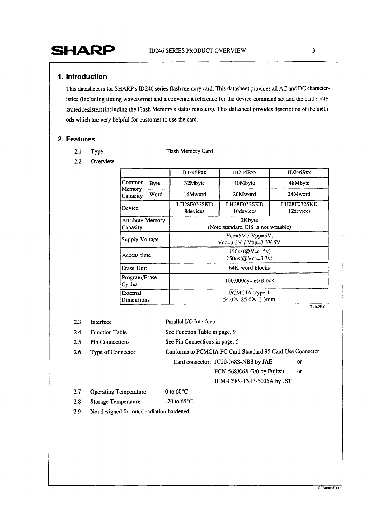
1. Introduction
This datasheet is for SHARP’s ID246 series flash memory card. This datasheet provides all AC and DC character-
istics (including timing waveforms) and a convenient reference for the device command set and the cards integrated registers(including the Flash Memory’s status registers). This datasheet provides description of the methods which are very helpful for customer to use the card.
2. Features
2.1 Type
2.2 Overview
2.3 Interface
Flash Memory Card
Common
Byte
Memory
Capacity Word
Device
Attribute Memory
Capasity
Supply Voltage
ID246Pxx ID246Rxx
ID246Sxx
32Mbyte
40Mbyte 48Mbyte
16Mword 20Mword 24Mword
LH28F032SKD
LH28F032SKD LH28F032SKD
8devices lodevices 12devices
2Kbyte
(Note:standard CIS is not writable)
vcc=sv ! vpp=sv,
vcc=3.3v I vpp=3.3v,5v
Access time
Erase Unit
Program/Erase
Cycles
External
Dimensions
150ns(@Vcc=%)
250ns(@Vcc=3.3v)
64K word blocks
1 OO,OOOcycles/Block
PCMCIA Type 1
54.0X 85.6X 3.3mm
Parallel I/O Interface
2.4 Function Table See Function Table in page. 9
2.5 Pin Connections
See Pin Connections in page. 5
2.6 Type of Connector
Conforms to PCMCIA PC Card Standard 95 Card Use Connector
Card connector: JC20-J68S-NB3 by JAE or
FCN-568J068-G/O by Fujitsu or
ICM-C68S-TS 13-5035A by JST
2.1 Operating Temperature 0 to 60°C
2.8 Storage Temperature -20 to 65°C
2.9
Not designed for rated radiation hardened.
Page 5
SHARP
ID246 SERIES PRODUCT OVERVlEW
3. Block Diagram
Control
Logic
zvcc
VPPl .
VPP2 ~
: :
:
I I I I
:
:
.
m
’ ’ - - - -
- - - -
VPP2 vcc
VPP 1 vcc
t t
Flash Memory Flash Memory
3 Data wP#k+ -bwP#
Data *’
.
e Add cE#l* + cm
Add 4
-Rp#
A
wE# 4---,
*WI3
RPWJ
STS OE# M
- OE#
STS -
/A
VPP2
t /I
vcc
VPP2
vcc
Flash Memory
b Data
wFJ# 4---
b Add cE# 4--**
wE# 4---(c
- STS
OE# 4i()--
Flash Memory
l w
Data * - -
+ cE#
Add + - -
l wE# RP#-+
* OE#
STS ---( ’
Figure 1. Block Diagram
Page 6
SHARP
ID246 SERIES PRODUCT OVERVIEW
5
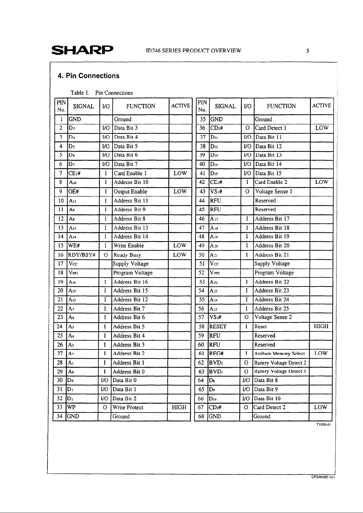
4. Pin Connections
Table 1. Pin Connections
T
I I
;r
SIGNAL I/O
I I
FUNCTION
ACTIVE
4
I I
;,” SIGNAL I/O
I I
FUNCTION
ACTIVE
LOW
LOW
HIGH
LOW
LOW
T1003-01
I
I
40 ~D,J
39 DIG
I I I
1 I/O IData Bit 14
1 I/O IData Bit 13
5 D6
6
D7
I/O Data Bit 6
I/O Data Bit 7
41 DIG
42 CEz#
I/O Data Bit 15
I Card Enable 2
7 CEI#
8 AIO
I Card Enable 1
I Address Bit 10
43 VSI#
44 RFU
0 Voltage Sense 1
Reserved
9 OE#
10 Al1
I Output Enable
I Address Bit 11
1 11 1As I I IAddress Bit9
I I 45 Imu
1 IReserved
I 1 1
15 IWE# I I I Write Enable
I
I
I I 1 Address Bit 20
I 16 IRDYTSSY# I o IReady
BUSY
LOW 1 1 50 IAx I I IAddress Bit 21
17 vcc
18
VPPI
Supply Voltage
Program Voltage
1 22
IA7
I I IAddress Bit7 1 1 56 IA25 I 1 (Address Bit 25
1 1 57 IVS2# I 0 IVoltage Sense 2 23 As
24 As
I Address Bit 6
I Address Bit 5 1 1 58 IkESET I I (Reset
25 A4
26 As
I Address Bit 4
I [Address Bit 3
-II
62 63 (BVD2 IBVD~
I 0 0 Battery Battery
Voltage Voltage Detect Detect 2
1
I 30 (Do I I/O (Data Bit 0
1 I/O (Data Bit 8
1 34 (GND
I
1 Ground
1 1
68
(GND
I
(Ground
I
CPSOQ08E.001
Page 7
SHARP
ID246 SERIES PRODUCT OVERVIEW 6
1
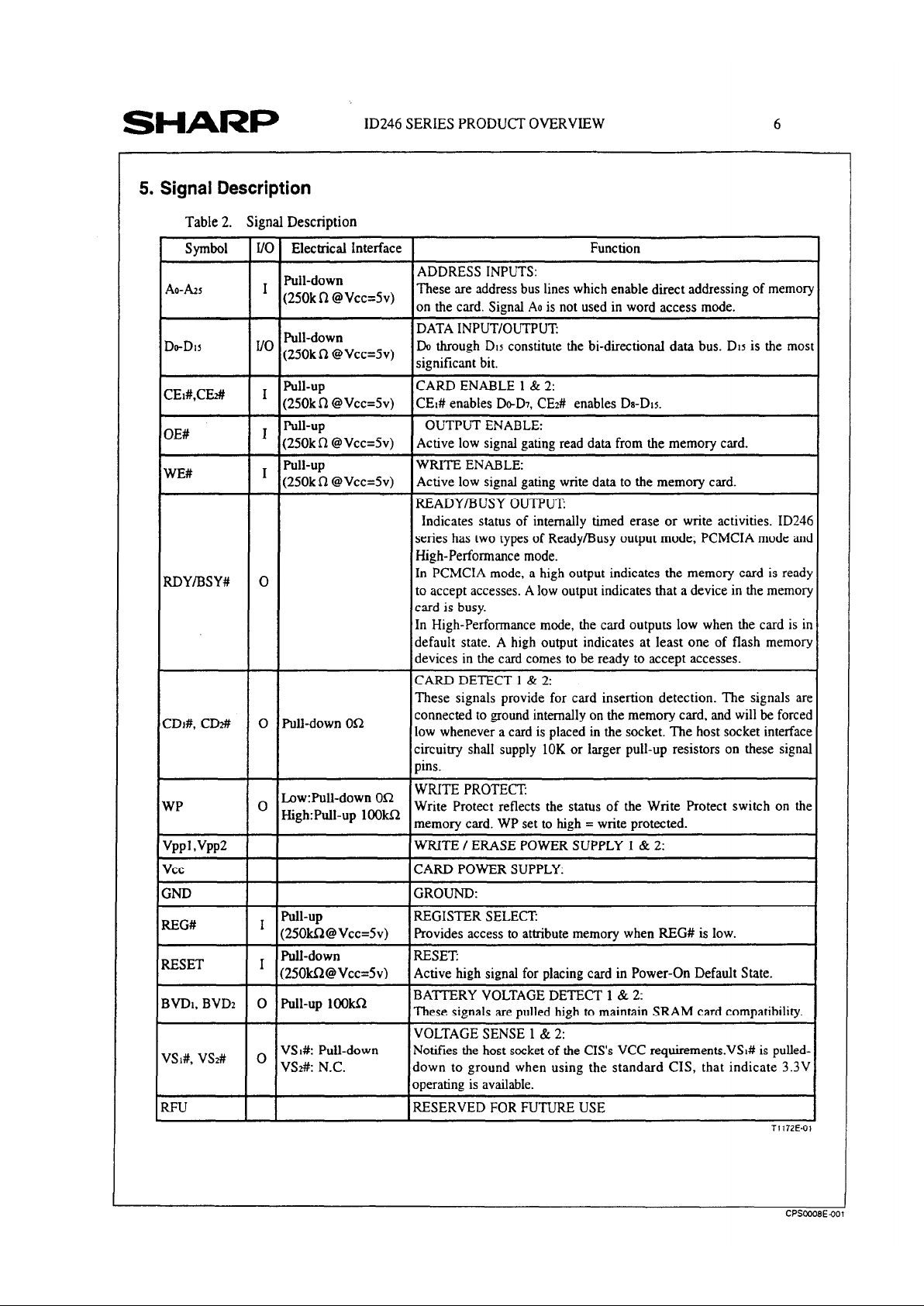
5. Signal Description
Table 2. Signal Description
Function
ADDRESS INPUTS:
40425
These are address bus lines which enable direct addressing of memory
on the card. Signal Ao is not used in word access mode.
DATA INPUT/OUTPUT
Do through DIG constitute the bi-directional data bus. Drs is the most
significant bit.
,,. Pull-down
I
(250kn @Vcc=Sv)
h-D15
CARD ENABLE 1 & 2:
CEI# enables D+D7, CE2# enables Da-DIG.
:Ei#,CEz#
>E#
OUTPUT ENABLE:
Active low signal gating read data from the memory card.
WRITE ENABLE:
Active low signal gating write data to the memory card.
READY/BUSY OUTPUp
NE#
Indicates status of internally timed erase or write activities. ID246
series has two types of Ready/Busy output mode; PCMCIA mode and
High-Performance mode.
In PCMCIA mode, a high output indicates the memory card is ready
to accept accesses. A low output indicates that a device in the memory
card is busy.
In High-Performance mode, the card outputs low when the card is in
default state. A high output indicates at least one of flash memory
devices in the card comes to be ready to accept accesses.
CARD DETECT 1 & 2:
0
IDYlBSY#
:DI#, CDz#
These signals provide for card insertion detection. The signals are
connected to ground internally on the memory card, and will be forced
low whenever a card is placed in the socket. The host socket interface
circuitry shall supply 10K or larger pull-up resistors on these signal
pins.
WRITE PROTECT:
0 Pull-down Of2
t
o Low:PuIl-down On
High:Pull-up 1OOkn
Write Protect reflects the status of the Write Protect switch on the
memory card. WP set to high = write protected.
I
VP
WRITE / ERASE POWER SUPPLY 1 & 2:
I
(PPI .VPP2
[cc CARD POWER SUPPLY:
I
iND
GROUND:
I
EG#
REGISTER SELECT:
Provides access to attribute memory when REG# is low.
RESET
Active high signal for placing card in Power-On Default State.
BATTERY VOLTAGE DETECT 1 & 2:
These signals are pulled high to maintain SRAM card compatibility.
VOLTAGE SENSE 1 & 2:
ESET
;VDI, BVDz 0 Pull-up 1ookQ
I
Notifies the host socket of the CIS’s VCC requirements.VS~# is pulledlawn to ground when using the standard CIS, that indicate 3.3V
operating is available.
RESERVED FOR FUTURE USE
T1172E.01
o VSI#: Pull-down
I
VS2#: N.C.
'Sl#, vs2#
CPS0008E40'
Page 8
SHARI=
ID246 SERIES PRODUCT OVERVIEW
7
6. Functions
6.1 Common Memory
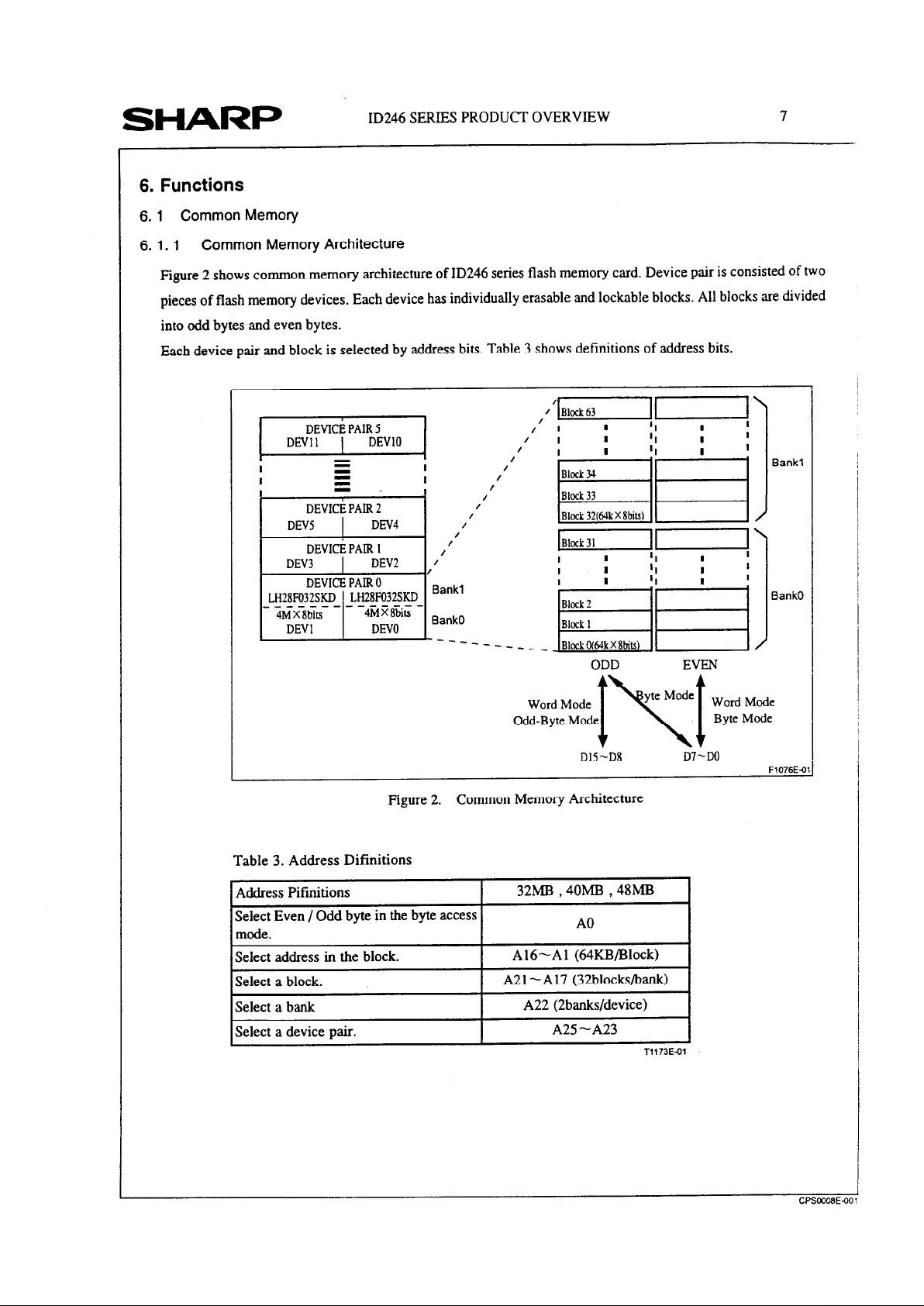
6. 1. 1 Common Memory Architecture
Figure 2 shows common memory architecture of ID246 series flash memory card. Device pair is consisted of two
pieces of flash memory devices. Each device has individually erasable and lockable blocks. All blocks are divided
into odd bytes and even bytes.
Each device pair and block is selected by address bits. Table 3 shows definitions of address bits.
DEVICE PAIR 5
DEVll 1 DEVIO
=
=
=
DEVICi PAIR 2
DEVS 1 DEV4
DEVIti PAIR 1
DEV3 1 DEV2
I
DEVICE PAIR 0
LH28FO32SKD LH28FO32SKD
- jGx-8&- - - -4;I z 8jjii DEVl DEVO
/
/
Bank1
Bank0
/’ Blodc63
/
/ 1
I
‘W
‘I I
/
I
I
‘I
I
I
1
Bank1
1
Bank0
ODD
EVEN
Word Mode
yte Mode
I\1
Word Mode
Odd-Byte Mode
Byte Mode
D15-D8 D7-DO
F1076E4)’
Figure 2. Common Memory Architecture
Table 3. Address Difinitions
Address Pifinitions 32MB ,4OMB ,48MB
Select Even / Odd byte in the byte access
A0
mode.
Select address in the block. A16-Al (64KJ3/Block)
Select a block.
A21 -A17 (32blocks/bank)
Select a bank
A22 (2banks/device)
Select a device pair. A25 -A23
T1173E-01
Page 9
SHARI=
ID246 SERIES PRODUCT OVERVIEW
8
6. 1.2 Erase
Erase is executed one block at a time. Erasable block size is 64K bytes in byte access mode and 128K bytes in
word access mode.
6. 1.3 Address Decoding
The higher address area of ID246 series flash memory card which goes beyond common memory area is not
decoded in common memory access. It means that the system will access to random memory address of the
memory card even if system will try to access to the memory address which exceeds memory capacity of the card.
Please do not access to the memory address which goes beyond memory capacity of the card.
As an enhanced function, the memory card enables to output invalid data (either of OOOOh or FFFFh) when system
will access to the memory address which exceeds memory capacity of the card. Please contact our sales & marketing support to find concrete way of setting.
6.2 Attribute Memory
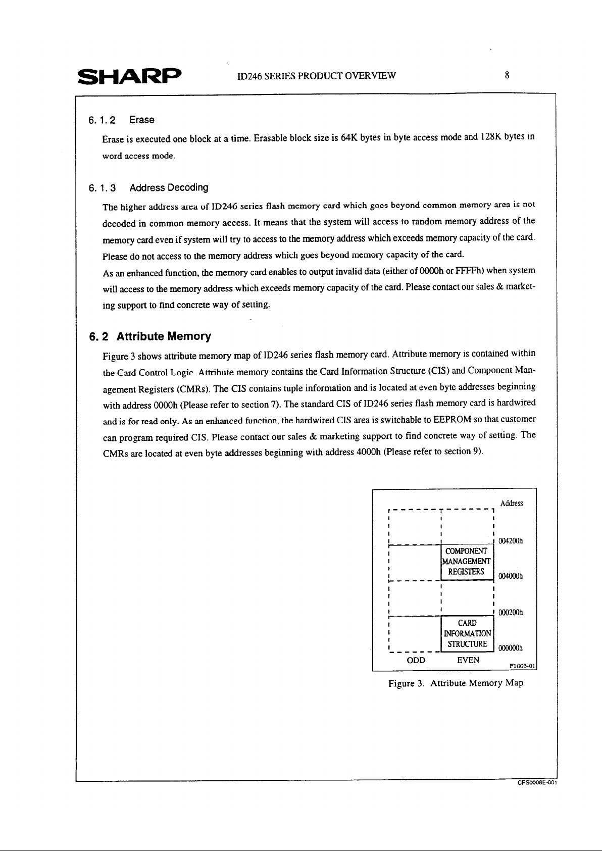
Figure 3 shows attribute memory map of ID246 series flash memory card. Attribute memory is contained within
the Card Control Logic. Attribute memory contains the Card Information Structure (CIS) and Component Management Registers (CMRs). The CIS contains tuple information and is located at even byte addresses beginning
with address OOOOh (Please refer to section 7). The standard CIS of ID246 series flash memory card is hardwired
and is for read only. As an enhanced function, the hardwired CIS area is switchable to EEPROM so that customer
can program required CIS. Please contact our sales & marketing support to find concrete way of setting. The
CMRs are located at even byte addresses beginning with address 4000h
(Please refer to section 9).
Address
,-“--’ T--“-‘,
ODD
EVEN
F1003-01
Figure 3. Attribute Memory Map
Page 10
SHARP
ID246 SERIES PRODUCT OVERVIBW
6.3 Function Table
6.3.1 Common Memory Access
Table 4. Common Memory
Mode
Stand-by
Byte Read
Word Read
Odd Byte Read
Byte Write
Word Write
Odd Byte write
tcess
H H L H H L Don’t care Odd
H L L X H L Odd Even
H L H X H L Odd Don’t care
6.3.2 Attribute Memory Access
Table 5. Attribute Memory Access
Mode REG# CE,# CE,# A, OE# WE# D,,, D
7-o
Stand-by
X H H X X X High-Z High-Z
L H L L L H
Even
Byte Read
High-Z
L H L H L H
High-Z xx
Word Read L L L X L H
xx Even
Odd Byte Read
Byte Write
Word Write
Odd Byte write
L L H X L H xx
High-Z
L H L L H L Don’t care
Even
L H L H H L
Don’t care Don’t care
L L L X H L Don’t care
Even
L L H X H L Don’t care
Don’t care
TS1059E-02
XX:Output data is invalid.
The standard CIS is for read only. Write operation is only for CMRs and CIS on EEPROM
7. Card Information Structure (CIS)
The CIS is contained within attribute memory (Please refer to section 6.2). Table 6 shows standard CIS tuples, but
it is for read only. As an enhanced function, the hardwired CIS area is switchable to EEPROM so that customer
can program required CIS. Please contact our sales & marketing support to find concrete way of setting.
Page 11
SHARP
ID246 SERIES PRODUCT OVERVIEW
Table 6. Standard CIS
Address
1 Value 1
Description
I
1 Address 1 Value
1 OOh 1 Olh
, 02h / 04h -1
1 46h 1 53h ISProduct Info
I
48h
4Ah
48h H
41h A Rash Memory
I
Access Time 150ns 4Ch 52h R
4Eh 50h P
I I
08h
7Eh
9Eh
Capacity
32MB
40MB
50h
52h
54h
56h
OOh END TEXT
4Yh I
4th D
32h 2
58h
34h 4
5Ah 53h S
5Ch
52h R
5Eh 20h SPACE
10h
12h
02h Conditions 3Vcc
57h Flash Memory
48h H
41h A
52h R
6Ah 1 50h IP
6Ch 1 20h ISPACE
60h
62h
64h
66h
6Xh
OOh ENDTEXT
53h S :Maker Info
Access Time 250ns
Capacity
32MB
40MB
48MB
End of Tuple
I I
1Ch
04h Tuple Link
I
43h C
4I=h 0
72h 1 52h IR
74h I 50h IP
6Eh
70h
1Eh ( 1Ph IROM
I
Access Time 200ns
Capacity 2KB
76h 1 4Fh 0
78h i 52h IR
End of Tuule
7Ah ( 41h A
7Ch 1 54h IT
28h 05h Tuple Link
2Ah 1 02h IConditions 3Vcc
ROM 1 2Cb 1 1Ph
7Eh
80h
82h
84h
86h
88h
8Ah
49h I
4I=h 0
4Eh N
OOh END TEXT
PFh End of Tuple
1 Ah Configuration Info
05h Tuple Link
2Eh
30h
32h
34h
36h
38h
3Ah
2Ab Access Time 2OOr-r~
Olh Capacity 2KB
PI% End of Tuple
18h JEDEC Code ID
02h Tuple Link
BOh Manufacture Code
DOh Device Code
Last Index of Configuration Table
3Ch
OOh End of Tuple
3Eh
15h Version Info Level 1
40h
23h Tuple Link
42h 04h Major Version
44h Olh Minor Version
CPS0008E401
Page 12
SHARP
ID246 SERIES PRODUCT OVERVIEW
Table 8. Standard CIS (Continued)
Address
1 Value 1 Description
I
9Ah
08h Tiple Link
9Ch
Olh Index
9Eh
02h
vcc & vpp
AOh
A2h
A4h
79h Parameter Selection
55h Vcc Voltage 5V
OCh ICC Static
A6h
A8h
06h ICC Average
06h ICC Peak
AAh 23h ICC Powerdown
ACh 1 1Bh 1 Contieuration Table Entrv 2 I
AEh
BOh
09h Tuple Link
02h Index
B2h
B4h
Olh Vcc Onry
79h Parameter Selection
B6h
B8h
B5h Vcc Voltage 5V
1Eh
BAh
BCh
BEh
OCh ICC Static
7Dh ICC Average
7Dh ICC Peark
COh 1 1Bh (ICC Powerdown
I
C2h
C4h
1Eh Device Geometry
06h Tuple Link
C6h 1 02h Bus
C8h 1 llh IErase
CAh ) Olh IRead size
I
CCh
CEh
Olh Write size
Olh Partation: lblock
DOh
D2h
0 1 h Non-interleaved
20h Manufacturer ID
D4h 1 04h ITunle Link
I
-+E-ta
Manufacturer Code
DEh
EOh
2 1 h Function Identification
02h Tuple Link
E2h
E4h
0 1 h Function: MEMORY
OOh System: None
E6h FFh End of CIS
I
CPS0008E-00
Page 13

SHARP
ID246 SERIES PRODUCT OVERVIEW
12
8. Card Control
8. 1 Reset
The card is in initial state directly after power-up. But we recommend to do reset operation after power-up to
make sure to initialize the card.
During block erase, byte write, or lock-bit configuration modes, an active RESET will abort the operation. RDYI
BSY# remains low until the reset operation completes. Memory contents being altered are no longer valid; the
data may be partially erased or written. The host must wait after RESET goes to logic-Low (VIL) before it can
write another command, as determined by tpt.nvL.
It is important to assert RESET to the card during a system reset. If a CPU reset occurs without a card reset, the
host will not be able to read from the card if that card is in a different mode when the system reset occurs.
For example, if an end-user initiates a host reset when the card is in read status register mode, the host will attempt
to read code from the card, but will actually read status register data. Sharp’s ID246 Series Flash Memory Card
allows proper card reset following a system reset through the use of the RESET input.
8. 2 Status Register
Each flash memory device in the card has status register. The status register may be read to determine when a
write, block erase, or lock-bits configuration is complete, and whether that operation completed successfully
(please refer to Table 7). It may be read at any time by writing the Read Status Register command (70h, 7070h)
into the CUI. In word access mode, the status register data of even byte devices are output to D7-0,and the status
register data of odd byte devices are output to D15-8.
8. 3 Write Protect Switch
The ID246 Series Flash Memory Card has a write protect switch on the back of the card. When the switch is in the
write protect position, the card blocks all writes to the common and attribute memory without Card Management
Registers region (see Figure 4 ).
8.4 Read Identifier Codes / Block Status Code
Manufacture Code and Device Code are contained within each flash memory device in the memory card. The
identifier code operation is initiated by writing the Read Identifier Codes command (90h, 9090h) into the CUI of
each memory device. The specific address of each device is necessary to be selected to read these codes (Table 9).
Writeble position
r
I
Write pro=sition
Note: The write protect switch is shown by the black square.
Figure 4. Write Protect Switch
CPSo@XEi)ol
Page 14

SHARP
ID246 SERIES PRODUCT OVERVIEW 13
Table 7(a). Status Register Definition
WSMS
7
BESS 1 ECBLBS 1 WSBLBS VPPS wss DPS R
6 5 4 3 2 1 0
NOTES:
SR.7 = WRITE STATE MACHINE STATUS
1 = Ready
Check RY/BY# pin or SR.7 to determine block erase, full
0 = Busy chip erase, (multi) word/byte write or block lock-bit
configuration completion.
SR.6 = BLOCK ERASE SUSPEND STATUS SR.6-0 are invalid while SR.7=“0”
1 = Block Erase Suspended
0 = Block Erase in Progress/Completed
If both SR.5 and SR.4 are “1”safter a block erase. full chip
erase,(multi) word/bite write, block lock-bit configuration or
SR.5 = ERASE AND CLEAR BLOCK LOCK-BITS STS configuration attempt, an improper command sequence
STATUS was entered.
1 = Error in Erase or Clear Block Lock-Bits
0 = Successful Erase or Clear Block Lock-Bit SR.3 does not provide a continuous indication of VPP
level. the WSM interrogates and indicates the VPP level only
5R.4 = WRITE AND SET BLOCK LOCK-BIT STATUS after block erase, full chip erase, (multi) word/byte write or
1 = Error in Write or Set Block Lock-Bit
block lock-bit configuration command sequences. SR.3 is
0 = Successful Write or Set Block Lock-Bit not guaranteed to reports accurate feedback only when
vPPi=vPPn
1.
SR.3 = VP? STATUS
1
= VPP
Low Detect, Operation Abort
SR. 1 does not provide a continuous indication of block
0 = VPP OK
lock-bit values. The WSM interrogates block lock-bit, and
WP# only after block erase, full chip erase, (multi)
3R.2 = WRITE SUSPEND STATUS
word/byte write or block lock-bit configuration command
1 = Write Suspended
sequences. Itinforms the system, depending on the
0 = Write in Progress/Completed
attempted operation, If the block lock-bit is set and/or WP#
is not
VIH.
Reading the block lock configuration codes after
jR. 1 = DEVICE PROTECT STATUS writing the Read Identifier Codes command indicates block
1 = Block Lock-Bit and/or WP# Lock Detected, lock-bit status.
Operation Abort
0 = Unlock
SR.0 is reserved for future use and should be masked out
when polling the status register.
3R.0 = RESERVED FOR FUTURJZ ENHANCEMENTS
TllfnC~n,
7 6 5 4 3 2 1 0
NOTES:
XSR.7 = STATE hlACHINE STATUS
1 =
Multi Word/byte Write
available
0 = Multi Word/byte Write not available
XSR.QO=RESERVED FOR FUTURE ENHANCEMENTS
After issue a Multi Word/Byte Write command: XSR.7
indicates that a next Multi Word/Byte Write command is
available.
XSR.B-0 is reserved for future use and should be masked
out when oolline the extended status register.
Page 15

SHARP
ID246 SERIES PRODUCT OVERVIEW
14
Table 8. Identifier Codes / Block Status
Select Device-pair Address in Device Even/Odd
Data Output D,-D,
k%1 hiA, A0
32MB ,4OMB, 48MB
Manufacture Identifier ooooOh
0:Even
Code
DPA
OCOOlh 1:Odd
BOh
Device Identifier Code DPA
00002h
00003h
0:Even
1 :Odd
DOh
Block Status Code
Block Status Code
DPA
XOOO4h
XOOO5h
(X: Select Block)
D,: O=Unlocked, l=Locked
D,: O=Last Erase operation
0:Even
completed successfully
1:Odd
l=Last Erase operation did
not completed successfully
D,-D,: Reserved
NOTE: A,, is ignored in word access mode, and D,5-D, outputs the Odd byte data.
DPA: Address as select device pair
BLKD: Block Lock Configuration Data
MLKD: Master Lock Configuration Data
Tl 1MEOl
Page 16

SHARP
ID246 SERIES PRODUCT OVERVIEW
9. Component Management Registers (CMR)
Component Management Registers (CMR) are mapped at even byte locations beginning at address 4000h in
attribute memory.
9. 1
9. 2
9. 3
9. 4
Configuration Option Register (Address:4000h)
Address Bit.7
Bit.6 Bit.5 Bit.4 Bit.3 Bit.2 Bit. 1 Bit.0
4000h SRESET
Reserved
SRESET: l=Reset State O=End Reset Cycle
Card Configuration Register (Address:4002h)
Address Bit.7
Bit.6 Bit.5 Bit.4 Bit.3
Bit.2 Bit. 1 Bit.0
4002h
Reserved
PWDN Reserved
PWDN: l=Power-Down
Device pairs that apointed by Sleep Control Register(4118h-411 Ah) are in PowerDown.
O=Power-Up
Socket and Copy Register (Address:4006h)
Address
Bit.7 Bit.6 Bit.5
4006h
Reserved Copy No.
Soket No.: Socket Number
Copy No.: Copy Number
Bit.4 Bit.3 Bit.2
Bit.1
Soket No.
Bit.0
I
The card may use to distinguish between similar cards installed in a system.
TlOL-01
Card Status Register (Address:41 OOh)
Address Bit7
Bit.6 Bit.5 Bit.4 Bit.3 Bit.2
Bit.1 Bit.0
4100h ADM
ADS SRESET CMWP PWDN
CISWP WP
RDYIBSY
ADM: ORed value of the Ready/Busy Mask Register.
1 = Any device is masked. 0 = All Devices are not Masked.
ADS: ORed
value
of the Sleep Control Register.
1 = Any device-pair is Controled power-down by bit.2 of the Card Configuration
Register.
SRESET: Reflects the bit.7 of the Configuration Option Register.
CMWP: Reflects the bit.1 of the Write Protection Register.
PWDN: Reflects the bit.2 of the Card Configuration Register.
CISWP: Reflects the bit.0 of the Write Protection Register.
WP: Indicates the Write Protect Switch status.
1 = Write Protect Switch: ON 1 = Write Protect Switch: OFF
RDY/BSY: Reflects the Ready/Busy Status Register.
1 = All devices are READY. 0 = Any device is BUSY.
TIO54-01
Page 17

SHARP
ID246 SERIES PRODUCT OVERVIEW
16
9. 5 Write Protection Register (Address:41 04h)
Address
4104h
Bit.7 Bit.6 Bit.5 Bit.4 Bit.3 Bit.2 Bit. 1
Reserved BLKEN CMWP
BLKEN: Block Locking Enable
1 = Enable Block Locking
0 = All Block Unlocked
Common Memory Write Protect
Bit.0
CISWP
CMWP: 1 = Common Memory without CIS region in Write Protect Status
Common Memory CIS Write Protect
CISWP: 1 = Common Memory CIS in Write Protect Status
TI 176E4l
9. 6 Sleep Control Register (Address:41 18h-411 Ah)
Address Bit.7 Bit.6 Bit.5 Bit.4 Bit.3 Bit.2 Bit. 1 Bit.0
411Al-l
Reserved
4118h Reserved DEV 10/l 1 DEV8/9 DEV6/7 DEV4/5 DEV2J3 DEVO/l
l= Select sleep mode device-pair
If set to “I”, the corresponding device-pairs are putted into deep powerdown mode
by PWDN bit of Configuration Status Register.
TIW741
9. 7 Ready/Busy Mask Register (Address:41 20h-4122h)
Address Bit.7
Bit.6 Bit.5 Bit.4 Bit.3 Bit.2 Bit.1 Bit.0
4122h Reserved DEVll DEVlO DEV9 DEV8
4120h DEV7
DEV6 DEVS 1 DEV4 DEV3 DEV2 DEVl DEVO
1 =Mask the Rdy/Bsy#
The corresponding device’s Rdy/Bsy# signals to set bit are ignored for cards
RDY/BSY# output.
9. 8 Ready/Busy Status Register (Address:41 30h-4132h)
Address
413231
4130h
Bit.7 Bit.6 Bit.5 Bit.4 Bit.3 Bit.2 Bit. 1 Bit.0
Reserved
DEVI 1 DEVIO DEV9 DEV8
DEV7
DEV6 DEVS
DEV4
DEV3 DEV2 DEVl DEVO
l=READY O=BUSY
Each bit indicates the corresponding device’s Rdy/Bsy# signal.
TlOIlOl
9.9 Ready/Busy Mode Register (Address:41 40h)
Address Bit.7 Bit.6 Bit.5 Bit.4 Bit.3 Bit.2 Bit.1 Bit.0
4140h Reserved RACK MODE
RACK: Ready Acknowledge Bit
Must clear this bit after receiving ready status to prepare for next device’s ready
transition.
MODE: RDY/BSY# Mode
1 = High-Performance Mode
0 = PCMCIA Mode
TIMSOL
Page 18

SHARP
ID246 SERIES PRODUCT OVERVIEW
10. Command Definitions
Device operations are determined by writing specific commands to the Command User Interface. Table 9 defines
the commands.
Table 9. Command Definitions
Read Identifier Codes
Word/Byte Write
Level-Mode for Erase and Write
(RY/BY# Mode)
STS Configuration
Pulse-Mode for Erase
write DA
B8h
(BSBSh)
Write DA
Olh
(OlOlh)
STS Configuration
B8h 02h
Pulse-Mode for Write
Write DA
(BSBSh)
Write DA
(0202h)
STS Configuration
Write DA
B8h
Write DA
03h
Pulse-Mode for Erase and Write
(BSBSh)
(0303h)
T115oE-m
Address
Data
IA
=Identifier cede Address ID =IdentiIier Codes
WA
=Write Address WD =Write Data
BA =Block Address SRD =Data from Status Register
DA =Device Address
QA
=Quety Offset Address
QD
=Data read
from Query database
Note:
1. Following the
Read Identifier Codes command, read operations access manufacture, device, block status
codes.
2. Status Register may be read to determine when a write, block erase, or lock bit configuration is complete,
and whether that operation completed successfully.
3. If the block is locked, block erase or write operations are desabled.
4. Following the Third Bus Cycle,inputs the write address and write data of ‘N’+l times.Finally, input the confirm
command ‘DOH’.
CP%008E40
Page 19

SHARP
ID246 SERIES PRODUCT OVERVIEW
10.1 Query Command
Query database can be read by writing Query comman
d (98H). Following the command write, read cycle from
address shown in Table 1 l-15 retrievethe critical information to write, erase and otherwise control the flash
component.
In word mode, Ds-Dis output the Query data of odd Byte Devices.
Table 10. Example of Query Structure Output
A,, A,, A,, A,, A,, A,
1 , 0 , 0 , 0 , 0 , 0 (20H)
X8 mode 1 , 0 , 0 , 0 , 0 , l(21H)
1 ,o,o,o, 1 ,oGw
1,0,0,0,1,1(23H)
A,, A,, A,, A,, A,
Xl6 mode l,O,O,O,O (10H)
1 ,O,O,O,l (11H)
Offset Address
(A6 - Al)
A0
0 = Even
1 = Odd
X
T
output
I
%-D*
High-z
High-Z
High-Z
High-Z
“Q”
“R”
D,-Do
“Q”
“Q”
“R”
“R”
“Q”
“R”
TllSZE-01
10. 1. 1 Block Status Register
This field provides lock configuration and erase status for the specified block. These informations are only avail-
able when device is ready (SR.7=1). If block erase or full chip erase operation is finished irregulary, block erase
status bit will be set to “l”,this block is invalid.
Table 11. Query Block Status Register
Offset
(Word Address)
Length
Description
(B A+2)H OlH Block Status Register
DO : Block Lock Configuration
O=Block is unlocked
l=Block is locked
Dl : Block Erase Status
O=Last erase operation completed successfully
l=Last erase operation not completed successfully
D2-7: Reserved for future use
NOTE: l.BA=The beginning of a Block Address.
T1153E41
Page 20

SHARI=
ID246 SERIES PRODUCT OVERVIEW 19
L
10. 1.2 CFI Query Identification String
The Identification String provides verification that the component supports the Common Flash Interface specifi-
cation. Additionally, If indicates which version of the spec and which Vendor-specified command set(s) istare)
supported.
Table 12. CR Query Identification String
Offset
(Word Address)
Length Description
lOH.1 lHJ2H
03H Query Unique ASCII string “QRY”
5 lH,52H,59H
13H,14H 02H Primary Vendor Command Set and Control Interfase ID Code
OlH,OOH (SCS ID Code)
15HJ6H 02H
Addressfor Primary Algorithm Extended Query Table
3 lH,OOH (SCS Extended Query Table Offset)
17HJ8H
02H Alternate Vendor Command Set and Control Interfase ID Code
OOOOH (OOOOH means that no alternate exists)
I9HJAH 02H
Address for Alternate Algorithm Extended Query Table
OOOOH (OOOOH means that no alternate exists)
T1154E-01
10. 1. 3 System Interface Information
The following device information can be useful in optimizing system interface software.
Table 13. System Information String
Offset
(Word Address)
IBH
Length
OlH
Description
V,, Logic Supply Minimum Write/Erase voltage
27H (2.7V)
LCH
. I
I
OlH V, Logic Supply Maximum Write/Erase voltage
55H (5.5V)
IDH
LEH
FH
!OH
!lH
!2H
!3H
!4H
!5H
:6H
OlH
OlH
OlH
OlH
OlH
OlH
OlH
OIH
OIH
OlH
V, Programming Supply Minimum Write/Erase voltage
27I.I (2.7V)
V, Programming Supply Maximum Write/Erase voltage
55H (5.5V)
Typical Timeout per Single Byte/Word Write
03H (23=8 usec)
Typical Timeout for Maximum Size Buffer Write (32 Bytes)
03H (2%4 usec)
Typical Timeout per Individual Block Erase
OAH (OAH=lO , 2i”=1024 msec)
Typical Timeout for Full Chip Erase
OFH (OFH=15 , 2iJ=32768 msec)
Maximum Timeout per Single Byte/Word Write, 2N times of typical
04H (r=16 , 8 usec x16=128 usec)
Maximum Timeout Maximum Size Buffer Write, 2N times of typical
04H (24=16, 64 usec x16=1024 usec)
Maximum Timeout per Individual Block Erase, 2N times of
typid
04H (2’=16, 1024 msec x16=16384 msec)
Maximum Timeout for Full Chip Erase, 2N times of typical
04H (24=16, 32768 msec x16=524288 msec)
T1155E.01
Page 21

SHARP
ID246 SERIES PRODUCT OVERVIEW 20
10. 1. 4 Device Geometry Definition
This field provides critical details of the flash device geometry.
Table 14. Device Geometry Definition
Offsel
(Word Address)
Length
I
Description
2lH OlH
28H. 29H 02H
2Ali. 2BH 02H
2CH OlH
2DH, 2EH 02H
2FH. 30H 02H
Device Size
15H (15H=21,22’=2097152=2M Bytes
Flash Device Interface description
02H,OOH (x8/x16 supports x8 and xl6 via BYlE#)
Maximum Number of Bytes in Multi word/byte write
05H.OOH (2’=32 Bytes)
Number of Erase Block Regions within device
01 H (symmetricatly blocked)
Tbe Number of Erase Blocks
lFH,OOH (lFH=31 =>31+1=32 Blocks
The Number of “256 Bytes” cluster in a Erase block
00H,OlH (OlOOH=256 =>256 Bytes x 256=643 Bytes in a Erase Block)
T1?5641
10. 1. 5 SCS OEM Specific Extended Query Table
Certain flash features and commands may be optional in a vendor-specific algorithm specification. The optional
vendor-specific Query table(s) may be used to specify this and other types of information. These structures are
defined solely by the flash vendor(s).
Table 15. SCS OEM Specific Extended Query Table
offset
(Word Address)
3lH,32H,33H
Length
03H
PRI
50H, 52H, 49H
Description
34H
35H
36H. 37H. 38H. 39H
OlH
OlH
04H
3 1 H (1) Major Version Number , ASCII
30H (0) Minor Version Number, ASCII
OFH, OOH, OOH, COH
Optional Command support
bitO=l : Chip Erase Supported
bitl=l : Suspend Erase Supported
b&2=1 : Suspend Write Supported
bit3=1 : Lock/Unlock Sqported
bit4=0 : Queued Erase. Not Supported
bit5-31=0 : reserved for future use.
3AH OIH OlH
Supported Functions after Suspend
bitO=l : Write Supported after Erase Suspend
bit l-7=0 : reserved for future use
3BH, 3CH 02H
03H, OOH
Block Status Register Mask
bitOr : Block Status Register Lock Bit (BSR.01 active
bitl=l : Block Status Register Valid Bit [BSR.l] active
biQ-15=0 : reserved for future use
3DH OlH
3EH OlH
3FH
reserved
Vcc Logic Supply Optimum Write/Erase voltage (highest performance)
50H (5.OV)
V, Progr amming Supply Optimum Write/Erase voltage (highest
performance)
50H (5.OV)
Reserved for future versions of the SCS Spccitication
rrrm-ot
Page 22

SHARP
ID246 SERIES PRODUCT OVERVIEW
21
10. 2 STS Configuration Command
The RDY/BSY# pin can be configured to different states using the STS Configuration command. Once the RDYI
BSY# pin has been configured, it remains in that configuration until another configuration command is issued, the
device is powered down or card is reset. Upon initial power-up and after exit from deep power-down mode. the
RDY/BSY# pin defaults to RY/BY# operation where STS low indicates that the WSM is busy. STS high indicates
that the WSM is ready for a new operation.
To reconfigure the RDY/BSY# pin to other modes, the STS Configuration is issued followed by the appropriate
configuration code. The three alternate configurations are all pulse mode for use as a system interrupt.
Table 16. STS Configuration Coding Description
Effects
Set STS pin to default level mode (RY/BY#). RY/BY# in the default level-mode of
operation will indicate WSM status condifion.
Set STS pin to plused output signal for specific erase operation. In this mode, STS
provides low pulse at the completion of Block Erase,Full Chip Erase and Clear Block
Lock-bit ooeration.
Set STS pin to pulsed output signal for a specific write operation. In this mode, STS
provides low pulse at the completion of (multi) Byte Write and Set Block Lock-bit
operation.
Set STS pin to pulsed output signal for specific write and erase operation.STS provides low
pulse at the completion of Block Erase, Full Chip Erase, (Multi) Word/Byte Configuration
operations.
T1158E-01
Table 17. Write Protection Alternatives
Operation
Block BLKEN bit of Write
Lock-Bit Protection Resister
Effect
Block Erase,
I
L
I
0 1 Block Erase and (Multi) Word/Byte Write
(Multi) Word/Byte
Write
h
Enabled.
1 I 1 Block is Locked. Block Erase and (Multi)
I
Word/Byte Write Disabled.
Full Chip Erase
Set Block Lock-Bit
Clear Block Lock-Bits
CL1
X
X
X
Block Lock-Bit Override. Block Erase and
(Multi) Word/Byte Write Enabled.
All unlocked blocks are erased, lockd blocks are
not erased.
All Block Lock-Bit
Disabled.
Set Block Lock-Bit Disabled.
Set Block Lock-Bit Enabled.
Clear Block Lock-Bit Disabled.
Clear Block Lock-Bit Enabled.
T1159E01
Page 23

SHARP
ID246 SERIES PRODUCT OVERVIEW 22
11. Electrical Specifications
11. 1 Absolute Maximum Ratings
PARAMETER
r
Supply Voltage
1
Program Voltage
~ Input Voltage
Operating Temperature
1 Storage Temperature
1
NOTE SYMBOL
RATING UNIT
2 V
V
cc
-0.3 to 6.0
2 V
PP
-0.2 to 7.0
V
2
vm
-0.3 to Vcc+0.3(Max:6.0) V
1 T
OPFC
0 to 60 ‘C
TSTG -20 to 65
‘c
T1165E41
NOTES:
1. Operating temperature is for commercial product defined by this specification.
2. All specified voltages are with respect to GND. During transitions, this level may undershoot to -2.0~ for
periods c20ns or overshoot to Vcc+2.Ov for periods <20ns.
11.2 Recommended Operating Coriditions
T1177E-01
11. 3 Capacitance
PARAMETER
Input Capacitance
Input/Output Capacitance
Ta=25 “c , f= 1 MHz
SYMBOL MIN TYP MAX UNIT
CONDITION
GIN -
15 -
PF
v,,=o.ov
50 -
25 -
PF
vo,=o.ov
11.4 AC Input/Output Test Conditions
Figure 5. Transient Input/Output Reference Waveform
Figure 5 shows Input/Output level and test level for AC test. Input rise and fall times (10% to 90%) < Ions.
Page 24

ID246 SERIES PRODUCT OVERVIEW
23
12. DC Characteristics
(Ta=Oto6O”C)
PARAMETER TEST CONDITION
Output High Voltage
Vcc Read Current
(Continue
to next page)
T1166E.01
Page 25

SHARP
ID246 SERLES PRODUCT OVERVIEW 24
DC Characteristics (Continued) (Ta = 0 to 60°C)
V,
Stand-by or Read
V, Deep Power-Down
Current
V,, Word Write or Set
Lock-Bit Current
V,, Block Erase or
Clear Lock-Bit Current
V, Word Write or
Block Erase Suspend
Current
V,, Lockout Voltage
NOTE:
SYM-
BOL
I
PPWS
4PES
V
-EL!5
TEST CONDITION
40MB 520 520 ,uA V&Vcc
48MB 5.50
550 6 ,u A
32MB 1.6 mA
40MB
2.0 mA v+vcc
48MB 2.4 mA
78
1.5 1.5 v
Tl lC7E-01
1. These parameters are applied to all input pins and all input/output pins in input mode.
2. These parameters are applied to AO-& and D,-Dn in input mode and RESET.
3. These parameters are applied to CE,#,CE,#,WB#,OE# and REG#.
4. These parameters are applied to RDY/BSY#.
5. These parameters are applied to D,-DrS in output mode.
6. All currents are in RMS unless otherwise notes.
7. Block erase, word/byte write, and lock-bit configurations are inhibited when V,s V,,, and guaranteed in
the V, Voltage is Vpp, , or V,.
8. Sampled.
CPS0008E-00
Page 26

SHARP
ID246 SERIES PRODUCT OVERVIEW
25
13. AC Characteristics
Testing Conditions :
1) Input Pulse Level
2) Input Rise/Fall Time
3) Input/Output Timing Reference Level
4) Output Load
(including scope and jig capacitance)
1.5 to 3.5v (@vcc=5vk5%,vcc=5v~lo%)
0 to 3.ov (@Vcc=3.3kOo.3V)
1Ons
2.5V (@Vcc=5V+5%,Vcc=5V+1oQ)
1.5v (@Vcc=3.3V&.3V)
I-I-l-L,+lOOpF ( @VCC=~V+~%,VCC=~V~IO%)
Il-I-L+SOpF (@Vcc=3.3V+O.3V)
13. 1 Common Memory Read Operations
(Ta = 0 to 60°C)
,
---- -BOL
vcc=3.3v+ 0.3v Vcc=SVk 5% 1 vcc=sv + 10%
[Jnit
*:Time until output becomes floating. (The output voltage is not defined.)
ns
TlC43-01
Page 27

SHARP
ID246 SERIES PRODUCT OVERVIEW
tFl
1
*
Address
t(A)
w
e
*
b(A)
w
CE#, CE2#
\
/
/
////
4
to3
OE#
Dout
Figure 6. AC Waveforms for Read Operations
Note) 1. WE# = “HIGH”, during a read cycle.
2. Either “HIGH” or “LOW” in diagonal areas.
3. The output data becomes valid when last interval, ta (A), ta (CE) or ta (OE) have concluded.
Page 28

SHARP
ID246 SERIES PRODUCT OVERVIEW
27
13.2 Command Write Operations : Common Memory
13. 2. 1 WE# Controlled Write Operations
PARAMETER
Write Cycle Time
Address Setup Time
Write
Recovery Time
Data
Setup Time for WE#
Data Hold Time
OE# Hold Time from
WE#
CE#
Setup Time for WE#
Address Setup Time for
WE#
Write Pulse Width
WE# High to RDY/BSY#
going Low
RESET Recovery Time
V, Setun Time
V, Hold Time
Word/Byte Write Time
Block Erase Time
Set Lock-Bit Time
Clear Block Lock-Bits
Time
Word/Byte
Suspend Latency
Time to Read
Erase Suspend Latency Tie
to Read
(Vcc=3.3V rtD.3\ I, Ta=O to 60°C)
SYMBOL
vcc=3.3v -tn ?V .“.a v
IEEE
1 PCMCIA
CONDITION
Unit
MIN
I
MAX
I
t t
*“A-J rW I
250
ns
30
ns
fwHQ”4
V,,=3.3VkO.3%
v,,=5v+lo% 10.0
S
V,,=3.3V~.3%
10.0
PS
$IHRHI
v,,=w *lo% 9.3
/IS
vPP=3.3vti.3%
21.1
PS
v,*=5v *lo% 17.2
P’s
T1168E-01
Page 29

SHARP
ID246 SERIES PRODUCT OVERVIEW
(Vcc=SVfi%, Vcc=5V+lO%,, Ta = 0 t
PARAMETER
OE# Hold Time from
Clear Block Lock-Bits
Erase Suspend Latency Tie
to Read
60°C )
~ Unit
~ ns
1 ns
ns
ns
ns
ns
ns
ns
ns
ns
P’s
ns
ns
PS
S
PS
S
1169E-01
CPSCW~E~IO
Page 30

SHARP
ID246 SERIES PRODUCT OVERVIEW
DATA
RDY/BSY#
RESET
Vu -
t 1
I \ u
I
th(oE-w-l!)
Wkl
VU
WHQVLZ.3.4
3
VIII ,
I-
VU
VU
WtIRHI.2
VOH
I
E
/
-4
I
VU
h
I I
VW12
VPP
VU
1. V,. POWER-UP AND STANDBY
2. WRITE DATA WRITE OR ERASE SETUP COMMAND
3. WRITE VALID ADDRESS AND DATA OR ERASE COMFIRM COMMAND
4. AUTOMATED DATA WRITE OR ERASE DELAY
5. READ STATUS REGISTER DATA
6. WRtTE READ ARRAY COMMAND
FIOIC-03
Figure 7. AC Waveforms for Write Operations (WE# Controlled)
Note)
While the data signal is in output mode, do not apply an opposite phase input signal.
Page 31

SHARP
ID246 SERIES PRODUCT OVERVIEW
13. 2. 2 CE# Controlled Write Operations
(Vcc=3,3V ti.3V, Ta = 0 to 60°C )
Erase Suspend Latency Tie
T1170E-01
Page 32

SHARP
ID246 SERIES PRODUCT OVERVIEW
31
PARAMETER
(Vcc=SV Y%, Vcc=SV MO%, Ta=O to 60°C
)
I’“VIIBOL
‘Yb
vcc=sv Y%
vcc=sv +-lo%
CONDITION Unit
IEEE
--_ _--.
KMCIA I
. I... . I. wr . . ..I
I,..,
Write Cycle Time t
A”.%”
Address Setup Time t
Write Recovery Time
LIZ
Data Setup Time for CE# bvEH
Data Hold Time
&HDx
OE# Hold Time from CE# acL
Write Pulse Width
b.EH
CE# High to RDY/BSY#
_
going LO*
hHRL
W)
I
t (cm I
1
80
1
- 1
80
I - I
ns I
1 - ( 140 1 - 1 140 1 ns 1
I
Clear Block Lock-Bits
Time
I I
kHQV.4
Word/Byte Suspend Latency
Time to Read
LRHl
v,=w *lo% - 7.0 - 7.0 p s
Erase Suspend Latency Tie
to Read
v,,=5v *lo% -
13.1 - 13.1 #us
T1171EQl
Page 33

SHARP
ID246 SERIES PRODUCT OVERVIEW
32
1. 2. 3.
4.
5.
6.
Address
AIN
I
VIII
tdA)- b
WE#
VIL
MOE-C’3
4
VIII
OEX
VU
hWE-CEH) i)-
e
lEHQVI.23.4
hi
31#, cm
VU.
VOH
I
tDYlJsY#
VOL
I
I
VIII
RESET
VLL
VPPl.2
VPP
VU
1. Vcc POWER-UP AND STANDBY
2. WRITr DATA WRITE OR ERASE SETUP COMMAND
3. WRITE VALID ADDRESS AND DATA OR ERASE COhtFlRh4 COMMAND
4. AUTOMATED DATA WRlTE OR ERASE DELAY
5. READ STATUS REGISTER DATA
6. WRITE READ ARRAY COMMAND
Figure 8.
AC Waveforms for Write Operations (CE# Controlled)
Note) While the data signal is in output mode, do not apply an opposite phase input signal.
Page 34

SHARP
ID246 SERIES PRODUCT OVERVIEW 33
13. 3 Attribute Memory Read Operation
(Ta=O-60°C)
PARAMETER
Read Cycle Time
Address Access Tie
SYMBOL
Vcc=3.3Vf 0.3v vcc=sv AZ 10%
Unil
IEEE
PCMCIA
MIN MAX MM MAX
t
AVAV
tcR 600 - 300 -
t
*w-w
L(A) -
600 - 300
CE# Access Time
OE# Access Time
Output Disable Time from CEl#,CE2# *
Output Disable Time from CE#
Output Disable Time from CE 1#,CE2#
Output Disable Time from OE#
Data
Valid Tie from Address Change
~ tm.Qv
f
GLQV
t
Ew2
t
GHPZ
fn ON7
I
wm
- 600 -
300
WEI
- 300 - 150
fdir(CE)
- 150 - 100
MOE)
- 150 - 100
Mm 5 - 5 -
ns
i t&9 IOI-Iol-I
1 I
I
I
I I I
* : Tie until becomes floating. (The output voltage is not defined)
T1056-G
Note) When the CIS constructed by EEPROM, this card requires 5V voltage for Vcc.
Address
CEl#, CE2#
/
I
OE#
/
hiiKE)
L&E) 4
I ta(OE) )
*
,.j
tdis(OE) ._
Dout
High-Inpedance
Data Output is valid
\\)
/I/
Figure 9. Attribute Memory Read Operation
CPSCWXE-001
Page 35

SHARP
ID246 SERIES PRODUCT OVERVIEW 34
13. 4 Attribute Memory Write Operation
(Ta=O-60°C)
i Address Setup Time
~ Write Recovery Time
1 data Setup Time
i Data Hold Time
/Address Setup Time for WE#
1 Write Pulse Width
Setup Time for OE#
Hold Tie for OE#
Setup Tie for CE#
Hold Time for CE#
SYMBOL
IEEE 1 PCMCIA
vcc=3.3v f 0.3v vcc=5vt 1070
MIN 1 MAX MIN 1 MAX
Unit
I
I I I I I I
t
AVAV
t
CW
1 600 1 - 1 250 - ns
LlAx L(WE)
70 - 30 - ns
t
DVWH
‘a@-WEH)
150 - 80
- ns
L UnY k@)
70 - 30 -
150 -
T1057.01
Note) When the CIS constructed by EEPROM, this card requires 5V voltage for Vcc.
Address
CEl#, CE2#
OE#
WE#
DATA
F1057-01
Figure 10. Attribute Memory Write Operation
Page 36

SHARP
ID246 SERIES PRODUCT OVERVIEW
13.5 Power-Up/Power Down
PARAMETER
CE# Signal Level (O.OV < Vcc < 2.OV)
CE# Signal Level (2.OV c Vcc c
VIH)
CE# Signal Level (VIH c Vcc)
CE# Setuo Time
RESET Setup Time
CE# Recover Time
VCC
Rising Time
VCC Falling Time
RESET Width
RESET Width
RESET Width
SYMBOL
PCMCIA
NOTES / MIN / MAX / UNITS /
Vi (CE) 1 0 ViMAX V
1 vcc-o. 1 Vih4AX V
1
VU4 Vih4AX
V
L” WCC) - 20 - ms
tsu (RESET) - 20 - ms
NOTES:
1. VM~ means Absolute Maximum Voltage for input in the period of O.OV < Vcc < 2.0 V, Vi (CE#) is only
o.oov-v&fAx
2. The tDr and tpf are defined as “linear waveforms” in the period of 10% to 9010, or vice-versa. Even if the
tb (Hi-Z RESET) - 1
-
ms
ts (Hi-Z RESET) - 0
-
ms
waveform is not a “liner waveform,” its rising and falling ime must meet this specification.
--
tsu (RESET) =
--
t,,
(Hi-z RESET)
Hi-Z-----------
3E1# yz5jK-J
ts (Hi-Z
RESET)
-------------_
Hi-Z
F1012-01
Figure Il. Power-Up/Down Timing
i
Page 37

SHARP
ID246 SERIES PRODUCT OVERVIEW
14. Specification Changes
This datasheet is for ID246 series product overview, and final specifications will be submitted for qualification of
the memory card. Please note that contents of this datasheet may be revised without announcement beforehand.
Please do NOT finalize a system design with this information.
15. Other Precautions
. Permanent damage occurs if the memory card is stressed beyond Absolute Maximum Ratings. Operation
beyond the Recommended Operating Conditions is not recommended and extended exposure beyond the
Recommended Operating Conditions may affect device reliability.
. Writing to the memory card can be prevented by switching on the write protect switch on the end of the
memory card.
. Avoid allowing the memory card connectors to come in contact with metals and avoid touching the connec-
tors, as the internal circuits can be-damaged by static electricity.
+ Avoid storing in direct sunlight, high temperatures (do not place near heaters or radiators), high humidity and
dusty areas.
. Avoid subjecting the memory card to strong physical abuse. Dropping, bending, smashing or throwing the
card can result in loss of function.
. When the memory card is not being used, return it to its protective case.
. Do not allow the memory card to come in contact with fire.
Page 38

SHARP
ID246 SERIES PRODUCT OVERVIEW
0
A ENLARGEMENT OF THE
WR I TE-PROTECT SW ITCH
I
16. External Diagrams
935
t68
1. b,, -
50. 8
II -
.
(Substrate Area)
1. 1
51. 8
I
FRONT
”
C
I
4
n
a
-
6kO.l
onncc t
Area)
\
3. 3 f0. 1 w
_I.
I I
\&
51. 8
\2-R2
cS"b¶trOtc Area)
BACK
Back
CPSWOGE-00
Protected
50. 8
1. 6
(fubrtrate Area) (fubrtrate Area)
1. 51 I- 41. 3
I I
TIIICKNESS
tlATERIAL
FINISH
MEMORY CAR0
NAME
EXTERNAL DIAGRAM
 Loading...