

Page 1
– 1 –
ICX080AK
E95518D99
Diagonal 6mm (Type 1/3) CCD Image Sensor for NTSC Color Video Cameras
Description
The ICX080AK is an interline CCD solid-state
image sensor suitable for NTSC color video
cameras. This chip conforms to DV standard SD
mode, and has the optimal number of pixels for
MPEG2 Main level. While achieving a horizontal
resolution of 450 TV lines, the area has been
expanded 33% in both vertical and horizontal
directions, making the chip suitable for electronic
vibration stabilizer and electronic panning/tilting. In
addition, complete 16:9 wide aspect ratio images
are provided with a high picture quality without
requiring vertical interpolation.
High sensitivity and low dark current are achieved
through the adoption of Ye, Cy, Mg and G
complementary color mosaic filters and HAD (HoleAccumulation Diode) sensors.
This chip features a field period readout system
and an electronic shutter with variable chargestorage time.
The package is a 16-pin DIP (Plastic), and both
top and bottom surface reference can be assured at
the same time.
Features
• Supports electronic vibration stabilizer and electronic panning/tilting
(33%/one side)
• Supports electronic zoom
• Supports DV standard SD mode and MPEG2 Main level (13.5MHz)
• Supports 16:9 wide aspect ratio (for both 18MHz and 5fsc)
• Supply voltage: 12V
• Horizontal register and reset gate: 2.7 to 3.6V drive
• No voltage adjustment (Reset gate and substrate bias are not adjusted.)
• High resolution, high sensitivity, low dark current and low smear
• Excellent antiblooming characteristics
• Continuous variable-speed shutter (1/60 to 1/10000s)
• Supports short exit pupil distance (Recommended range: –20 to –100mm)
• Ye, Cy, Mg and G complementary color mosaic filters on chip
• 16-pin high precision plastic package (both top and bottom surface reference possible)
Device Structure
• Interline CCD image sensor
• Image size: Diagonal 6mm (Type 1/3)
• Total number of pixels: 1016 (H) x 674 (V) approx. 680K pixels
• Total number of effective pixels: 962 (H) x 654 (V) approx. 630K pixels
• Number of effective pixels: 4:3 NTSC: 711 (H) x 485 (V) approx. 340K pixels
16:9 18MHz: 948 (H) x 485 (V) approx. 460K pixels
16:9 5fsc: 942 (H) x 485 (V) approx. 460K pixels
• Chip size: 5.90mm (H) x 4.92mm (V)
• Unit cell size: 5.05µm (H) x 5.55µm (V)
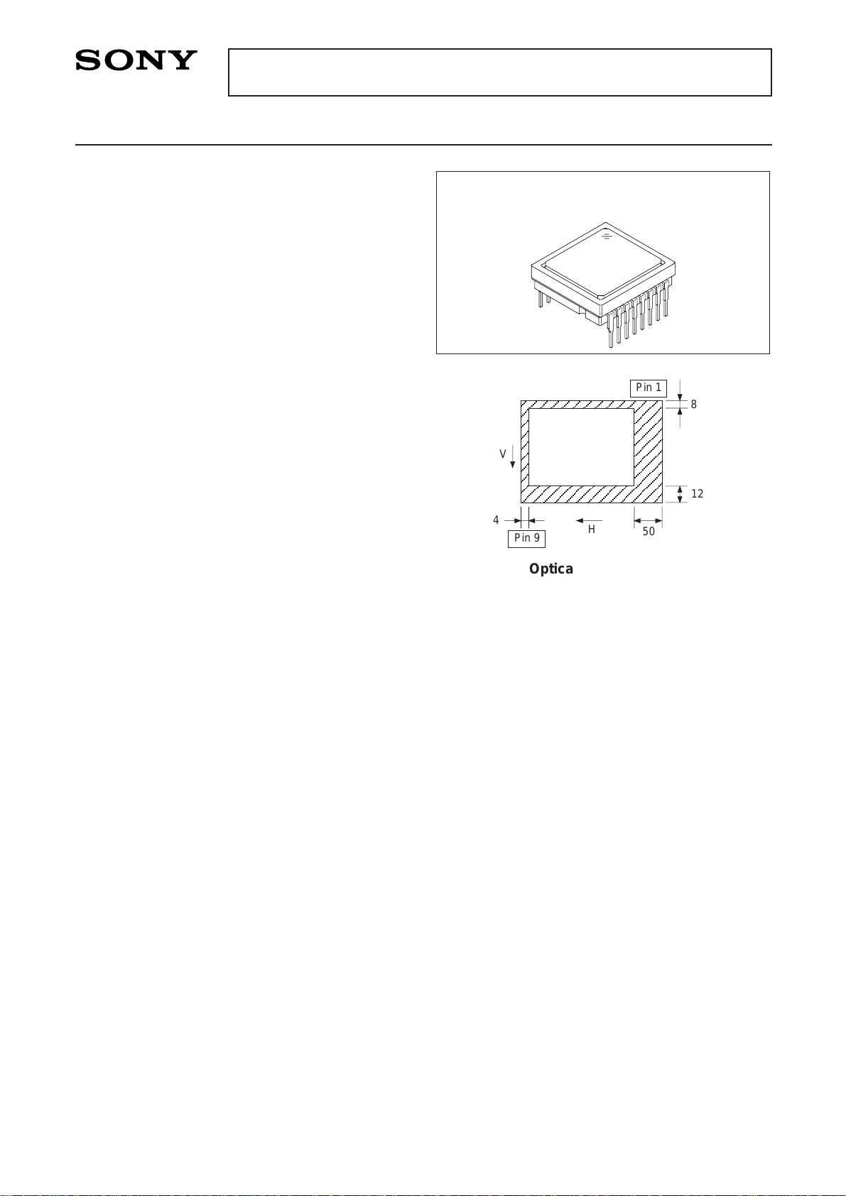
• Optical black: Horizontal (H) direction: Front 4 pixels, rear 50 pixels
Vertical (V) direction: Front 12 pixels, rear 8 pixels
• Number of dummy bits: Horizontal 28
Vertical 1 (even fields only)
• Substrate material: Silicon
Sony reserves the right to change products and specifications without prior notice. This information does not convey any license by
any implication or otherwise under any patents or other right. Application circuits shown, if any, are typical examples illustrating the
operation of the devices. Sony cannot assume responsibility for any problems arising out of the use of these circuits.
16 pin DIP (Plastic)
A
A
Pin 1
V
4
50
8
12
Pin 9
H
Optical black position
(Top View)
AAAA
AAAA
Page 2
– 2 –
ICX080AK
Against φSUB
Against GND
Against VL
Between input clock
pins
Storage temperature
Operating temperature
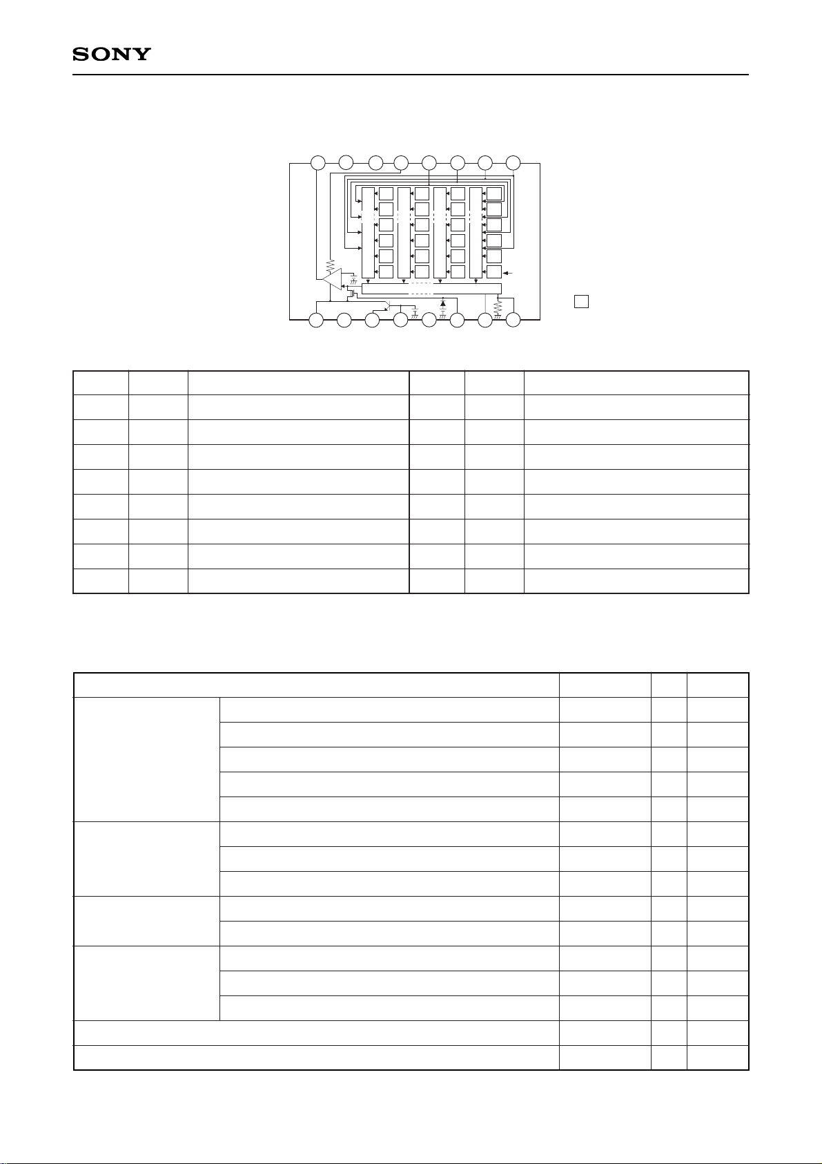
Block Diagram and Pin Configuration
(Top View)
Note) : Photo sensor
V
OUT
GND
GND
GND
Vφ
1
Vφ
2
Vφ
3
Vφ
4
V
DD
GND
φSUB
C
SUB
V
L
φRG
Hφ
1
Hφ
2
Ye
G
Ye
Mg
Ye
G
Cy
Mg
Cy
G
Cy
Mg
Ye
G
Ye
Mg
Ye
G
Cy
Mg
Cy
G
Cy
Mg
Horizontal Register
Note)
Vertical Register
1
2
3
4
5
6
7
8
9
10
11
12
13
14 15
16
Pin No.
1
2
3
4
5
6
7
8
Vφ4
Vφ3
Vφ2
Vφ1
GND
GND
GND
VOUT
Vertical register transfer clock
Vertical register transfer clock
Vertical register transfer clock
Vertical register transfer clock
GND
GND
GND
Signal output
9
10
11
12
13
14
15
16
VDD
GND
φSUB
CSUB
VL
φRG
Hφ1
Hφ2
Supply voltage
GND
Substrate clock
Substrate bias
∗1
Protective transistor bias
Reset gate clock
Horizontal register transfer clock
Horizontal register transfer clock
Symbol Description
Pin Description
Absolute Maximum Ratings
–40 to +10
–50 to +15
–50 to +0.3
–40 to +0.3
–25 to
–0.3 to +18
–10 to +18
–10 to +5
–0.3 to +28
–0.3 to +15
to +15
–5 to +5
–13 to +13
–30 to +80
–10 to +60
V
V
V
V
V
V
V
V
V
V
V
V
V
°C
°C
VDD, VOUT, φRG – φSUB
Vφ1, Vφ3 – φSUB
Vφ2, Vφ4, VL – φSUB
Hφ1, Hφ2, GND – φSUB
CSUB – φSUB
VDD, VOUT, φRG, CSUB – GND
Vφ1, Vφ2, Vφ3, Vφ4 – GND
Hφ1, Hφ2 – GND
Vφ1, Vφ3 – VL
Vφ2, Vφ4, Hφ1, Hφ2, GND – VL
Voltage difference between vertical clock input pins
Hφ1 – Hφ2
Hφ1, Hφ2 – Vφ4
Item Ratings Unit Remarks
∗2
+24V (Max.) when clock width < 10µs, clock duty factor < 0.1%.
∗1
DC bias is generated within the CCD, so that this pin should be grounded externally through a capacitance
of 0.1µF.
∗2
Pin No. Symbol Description
Page 3
– 3 –
ICX080AK
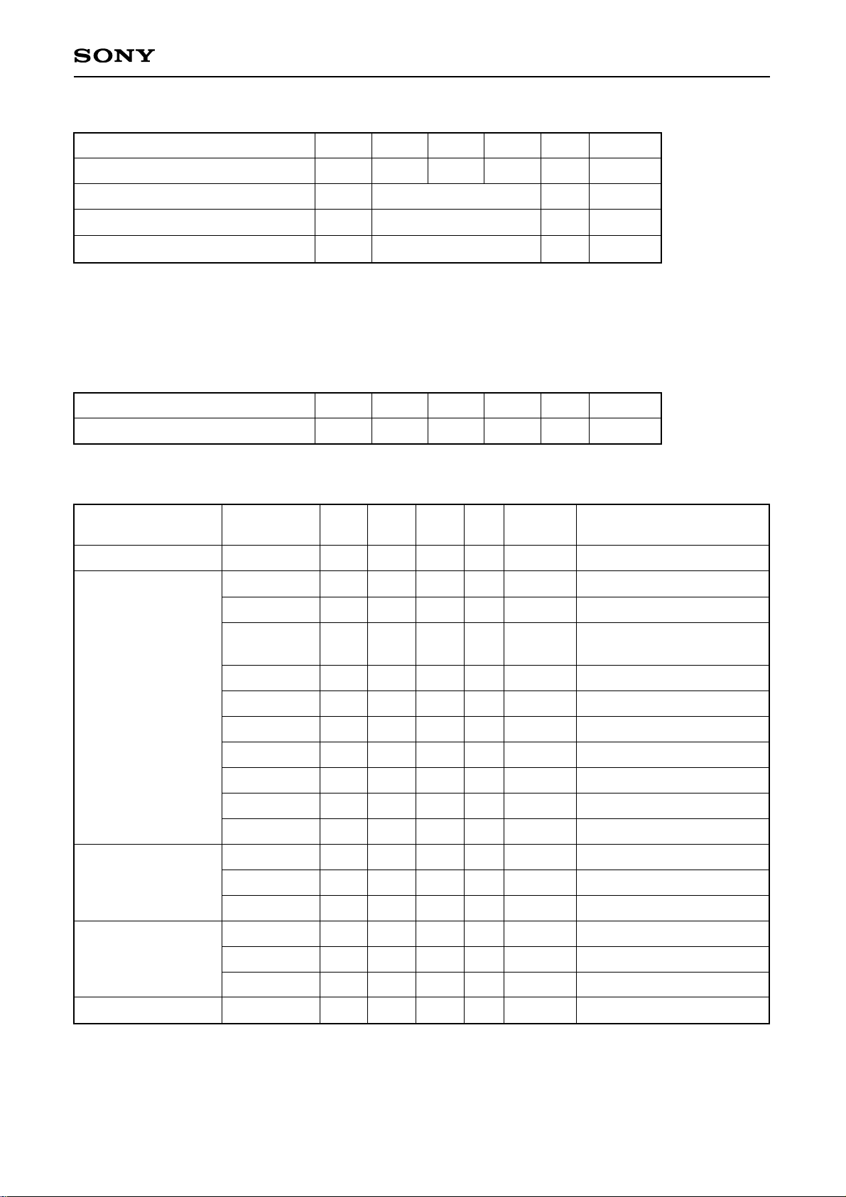
Clock Voltage Conditions
Item
Readout clock voltage
VVT
VVH1, VVH2
VVH3, VVH4
VVL1, VVL2,
VVL3, VVL4
VφV
VVH3 – VVH
VVH4 – VVH
VVHH
VVHL
VVLH
VVLL
VφH
VHL
VCR
VφRG
VRGLH – VRGLL
VRGL – VRGLm
VφSUB
11.64
–0.05
–0.2
–6.85
5.95
–0.25
–0.25
2.7
–0.05
0.5
2.7
17.3
12.0
0
0
–6.5
6.5
3.3
0
1.65
3.3
18.5
12.36
0.05
0.05
–6.15
6.9
0.1
0.1
0.5
0.5
0.5
0.5
3.6
0.05
3.6
0.4
0.5
19.3
V
V
V
V
V
V
V
V
V
V
V
V
V
V
V
V
V
V
1
2
2
2
2
2
2
2
2
2
2
3
3
3
4
4
4
5
VVH = (VVH1 + VVH2)/2
VVL = (VVL3 + VVL4)/2
VφV = VVHn – VVLn (n = 1 to 4)
High-level coupling
High-level coupling
Low-level coupling
Low-level coupling
Cross-point voltage
Low-level coupling
Low-level coupling
Horizontal transfer
clock voltage
Reset gate clock
voltage
Substrate clock voltage
Vertical transfer clock
voltage
Symbol Min. Typ. Max. Unit
Waveform
diagram
Remarks
Bias Conditions
Item
Supply voltage
Protective transistor bias
Substrate clock
Reset gate clock
VDD
VL
φSUB
φRG
11.64
12.0
∗1
∗2
∗2
12.36
V
Symbol Min. Typ. Max. Unit Remarks
DC Characteristics
Item
Supply current IDD 6.0 mA
Symbol Min. Typ. Max. Unit Remarks
∗1
VL setting is the VVL voltage of the vertical transfer clock waveform, or the same power supply as the VL
power supply for the V driver should be used.
∗2
Do not apply a DC bias to the substrate clock and reset gate clock pins, because a DC bias is generated
within the CCD.
Page 4
– 4 –
ICX080AK
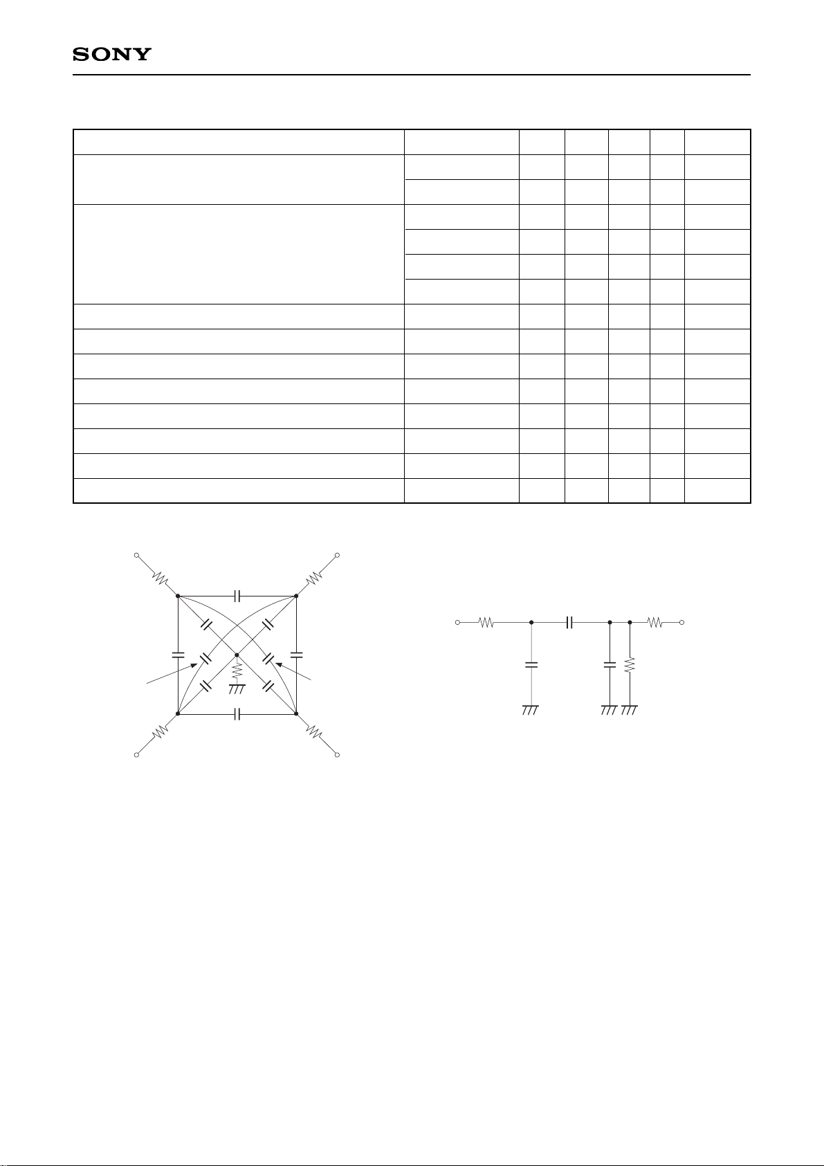
Clock Equivalent Circuit Constant
Item
Capacitance between vertical transfer clock and
GND
CφV1, CφV3
CφV2, CφV4
CφV12, CφV34
CφV23, CφV41
CφV13
CφV24
CφH1, CφH2
CφHH
CφRG
CφSUB
R1, R2, R3, R4
RGND
RφH
RH2
1000
560
470
390
180
100
62
62
12
270
82
15
3
30
pF
pF
pF
pF
pF
pF
pF
pF
pF
pF
Ω
Ω
Ω
kΩ
Capacitance between vertical transfer clocks
Capacitance between horizontal transfer clock and GND
Capacitance between horizontal transfer clocks
Capacitance between reset gate clock and GND
Capacitance between substrate clock and GND
Vertical transfer clock series resistor
Vertical transfer clock ground resistor
Horizontal transfer clock series resistor
Horizontal transfer clock ground resistor
Symbol Min. Typ. Max. Unit Remarks
RφH RφH
Hφ2Hφ1
CφH1 CφH2
CφHH
Vφ1
CφV12
Vφ2
Vφ4 Vφ3
CφV34
CφV23CφV41
CφV13
CφV24
CφV1 CφV2
CφV4 CφV3
RGND
R4
R1
R3
R2
Vertical transfer clock equivalent circuit Horizontal transfer clock equivalent circuit
RH2
Page 5
– 5 –
ICX080AK
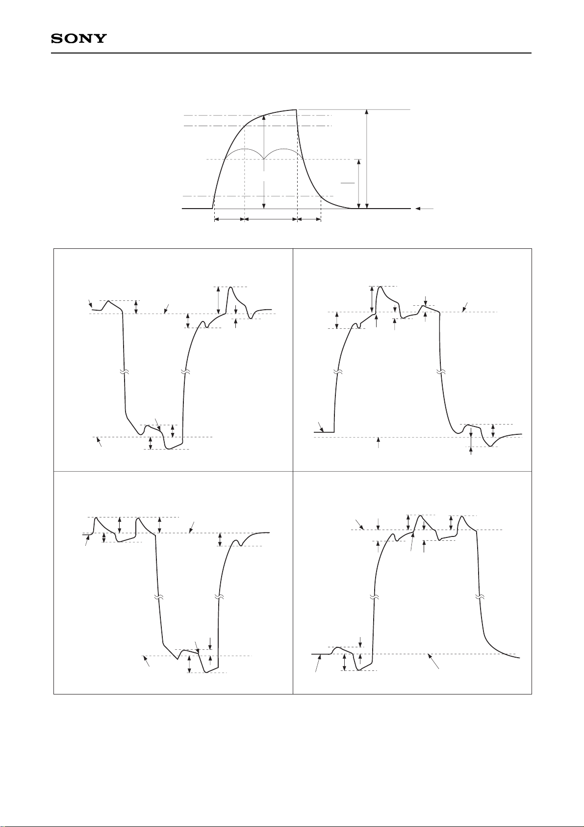
Drive Clock Waveform Conditions
(1) Readout clock waveform
(2) Vertical transfer clock waveform
II II
100%
90%
10%
0%
VVT
tr twh tf
φM
0V
φM
2
Vφ1 Vφ3
Vφ2 Vφ4
VVHH
VVH
VVHL
VVHH
VVHL
VVH1
VVL1
VVLH
VVLL
VVL
VVHH
VVH3
VVHL
VVH
VVHH
VVHL
VVL3
VVL
VVLL
VVLH
VVHH VVHH
VVH
VVHL
VVHL
VVH2
VVLH
VVL2
VVLL
VVL
VVHH VVHH
VVHL
VVH4
VVHL
VVH
VVL
VVLH
VVLL
VVL4
VVH = (VVH1 + VVH2)/2
VVL = (VVL3 + VVL4)/2
VφV = VVHn – VVLn (n = 1 to 4)
Page 6
– 6 –
ICX080AK
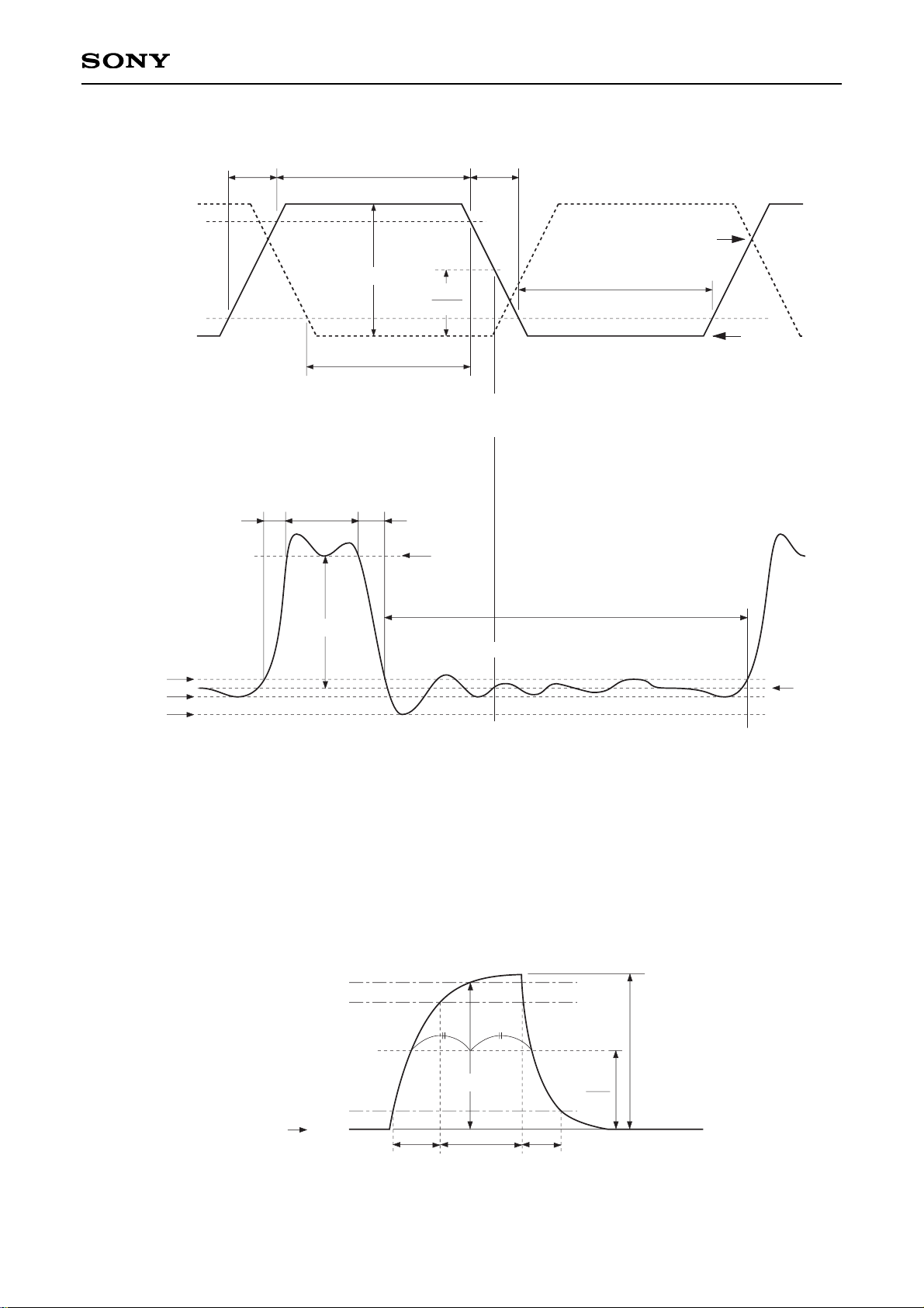
twh tftr
90%
10%
V
HL
twl
Hφ1
two
Hφ2
VRGL
VRGLL
VRGLH
twl
V
RGH
RG waveform
VRGLm
tr twh tf
V
CR
Point A
(3) Horizontal transfer clock waveform
Cross-point voltage for the Hφ1 rising side of the horizontal transfer clocks Hφ1 and Hφ2 waveforms is VCR.
The overlap period for twh and twl of horizontal transfer clocks Hφ1 and Hφ2 is two.
(4) Reset gate clock waveform
VφH
VφH
2
VφRG
VRGLH is the maximum value and VRGLL is the minimum value of the coupling waveform during the period from
Point A in the above diagram until the rising edge of RG. In addition, VRGL is the average value of VRGLH and
VRGLL.
VRGL = (VRGLH + VRGLL) /2
Assuming VRGH is the minimum value during the interval twh, then:
VφRG = VRGH – VRGL.
Negative overshoot level during the falling edge of RG is VRGLm.
(5) Substrate clock waveform
90%
100%
10%
0%
V
SUB
tr twh tf
φM
φM
2
(A bias generated within the CCD)
VφSUB
Page 7
– 7 –
ICX080AK
Clock Switching Characteristics
Item
Readout clock
Vertical transfer
clock
Reset gate clock
Substrate clock
VT
Vφ1, Vφ2,
Vφ3, Vφ4
Hφ1
Hφ2
Hφ1
Hφ2
φRG
φSUB
1.36
14
14
7
1.7
1.56
19.5
19.5
5.56
10
3.06
141419.5
19.5
5.56
37
0.5
8.5
8.5
0.01
0.01
4
14
14
0.5
15
0.5
8.5
8.5
0.01
0.01
5
250
14
14
0.5
µs
ns
ns
µs
ns
µs
During
readout
During
CXD1267AN
used
tf ≥ tr – 2ns
During
drain
charge
Symbol
twh
Min. Typ. Max. Min. Typ. Max. Min. Typ. Max. Min. Typ. Max.
twl tr tf
Unit Remarks
Horizontal
transfer clock
During
imaging
During
parallel-serial
conversion
Item
Horizontal transfer clock
Hφ1, Hφ2
12 19.5 ns
Symbol
two
Min. Typ. Max.
Unit Remarks
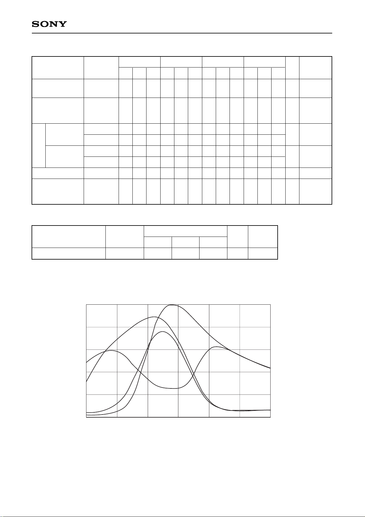
Spectral Sensitivity Characteristics (excludes both lens characteristics and light source characteristics)
1.0
0.8
0.6
0.4
0.2
0.0
450400 500 550 600 650 700
Relative Response
Wave Length [nm]
Mg
Cy
Ye
G
Page 8
– 8 –
ICX080AK
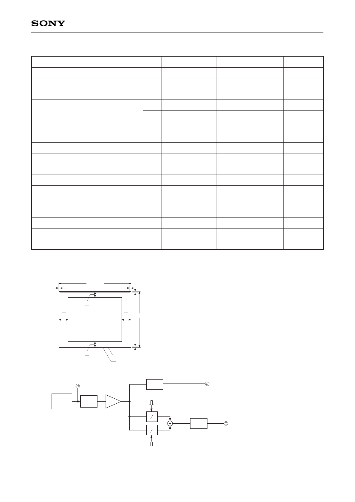
Zone Definition of Video Signal Shading
6
8
654 (V)
1414
962 (H)
V
10
H
8
H
8
V
10
Ignored region
Zone 0, I
Zone II, II'
Effective pixel region
Measurement System
CCD C.D.S
LPF1
LPF2
S
H
AMP
CCD signal output
Y signal output
Chroma signal output
(3dB down 8MHz)
(3dB down 1MHz)
[∗Y]
[∗C]
[∗A]
S
H
Note) Adjust the amplifier gain so that the gain between [∗A] and [∗Y], and between [∗A] and [∗C]
equals 1.
∗1
Excludes vertical dark signal shading caused by vertical register high-speed transfer.
Image Sensor Characteristics (Ta = 25°C)
Item
Sensitivity
Saturation signal
Smear
Video signal shading
Uniformity between video
signal channels
Dark signal
Dark signal shading
Flicker Y
Flicker R-Y
Flicker B-Y
Line crawl R
Line crawl G
Line crawl B
Line crawl W
Lag
S
Ysat
Sm
SHy
∆Sr
∆Sb
Ydt
∆Ydt
Fy
Fcr
Fcb
Lcr
Lcg
Lcb
Lcw
Lag
240
600
300
0.009 0.015
20
25
10
10
2
1
2
5
5
3
3
3
3
0.5
mV
mV
%
%
%
%
%
mV
mV
%
%
%
%
%
%
%
%
1
2
3
4
4
5
5
6
7
8
8
8
9
9
9
9
10
Ta = 60°C
Zone 0 and I
Zone 0 to II'
Ta = 60°C
Ta = 60°C,
∗1
Symbol Min. Typ. Max. Unit Measurement method Remarks
Page 9
– 9 –
ICX080AK
Image Sensor Characteristics Measurement Method
Measurement conditions
1) In the following measurements, the device drive conditions are at the typical values of the bias and clock
voltage conditions.
2) In the following measurements, spot blemishes are excluded and, unless otherwise specified, the optical
black level (OB) is used as the reference for the signal output, which is taken as the value of Y signal
output or chroma signal output of the measurement system.
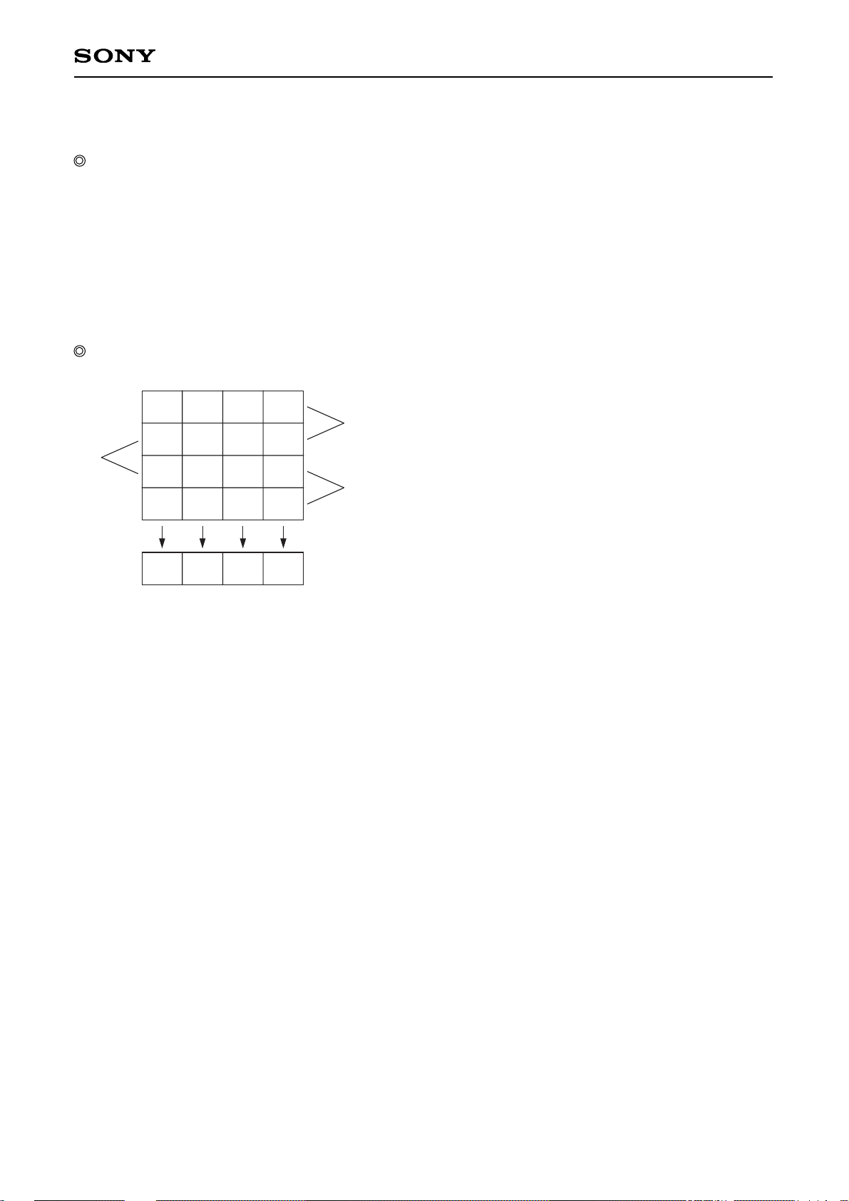
Color coding of this image sensor & Composition of luminance (Y) and chroma (color difference) signals
As shown in the left figure, fields are read out. The charge is
mixed by pairs such as A1 and A2 in the A field. (pairs such
as B in the B field)
As a result, the sequence of charges output as signals from
the horizontal shift register (Hreg) is, for line A1, (G + Cy),
(Mg + Ye), (G + Cy), and (Mg + Ye).
These signals are processed to form the Y signal and chroma (color difference) signal. The Y signal is formed
by adding adjacent signals, and the chroma signal is formed by subtracting adjacent signals. In other words,
the approximation:
Y= {(G + Cy) + (Mg + Ye)} x 1/2
= 1/2 {2B + 3G +2R}
is used for the Y signal, and the approximation:
R – Y = {(Mg + Ye) – (G + Cy)}
= {2R – G}
is used for the chroma (color difference) signal. For line A2, the signals output from Hreg in sequence are
(Mg + Cy), (G + Ye), (Mg + Cy), (G + Ye).
The Y signal is formed from these signals as follows:
Y= {(G + Ye) + (Mg + Cy)} x 1/2
= 1/2 {2B + 3G +2R}
This is balanced since it is formed in the same way as for line A1.
In a like manner, the chroma (color difference) signal is approximated as follows:
–(B – Y) = {(G + Ye) – (Mg + Cy)}
= – {2B – G}
In other words, the chroma signal can be retrieved according to the sequence of lines from R – Y and –(B – Y)
in alternation. This is also true for the B field.
Cy Ye
G
Mg
Cy Ye
G
Mg
Cy Ye
G
Mg
Cy Ye
G
Mg
A1
A2
B
Hreg
Color Coding Diagram
Page 10
– 10 –
ICX080AK
Definition of standard imaging conditions
1) Standard imaging condition I:
Use a pattern box (luminance 706cd/m2, color temperature of 3200K halogen source) as a subject.
(Pattern for evaluation is not applicable.) Use a testing standard lens with CM500S (t = 1.0mm) as an IR
cut filter and image at F5.6. The luminous intensity to the sensor receiving surface at this point is defined
as the standard sensitivity testing luminous intensity.
2) Standard imaging condition II:
Image a light source (color temperature of 3200K) with a uniformity of brightness within 2% at all angles.
Use a testing standard lens with CM500S (t = 1.0mm) as an IR cut filter. The luminous intensity is
adjusted to the value indicated in each testing item by the lens diaphragm.
3) Standard imaging condition III:
Image a light source (color temperature of 3200K) with a uniformity of brightness within 2% at all angles.
Use a testing standard lens (exit pupil distance –33mm) with CM500S (t = 1.0mm) as an IR cut filter. The
luminous intensity is adjusted to the value indicated in each testing item by the lens diaphragm.
1. Sensitivity
Set to standard imaging condition I. After selecting the electronic shutter mode with a shutter speed of
1/250s, measure the Y signal (Ys) at the center of the screen and substitute the value into the following
formula.
S = Ys x [mV]
2. Saturation signal
Set to standard imaging condition II. After adjusting the luminous intensity to 10 times the intensity with
average value of the Y signal output, 200mV, measure the minimum value of the Y signal.
3. Smear
Set to standard imaging condition II. With the lens diaphragm at F5.6 to F8, adjust the luminous intensity
to 500 times the intensity with average value of the Y signal output, 200mV. When the readout clock is
stopped and the charge drain is executed by the electronic shutter at the respective H blankings,
measure the maximum value YSm [mV] of the Y signal output and substitute the value into the following
formula.
4. Video signal shading
Set to standard imaging condition III. With the lens diaphragm at F5.6 to F8, adjust the luminous intensity
so that the average value of the Y signal output is 200mV. Then measure the maximum (Ymax [mV]) and
minimum (Ymin [mV]) values of the Y signal and substitute the values into the following formula.
SHy = (Ymax – Ymin)/200 x 100 [%]
5. Uniformity between video signal channels
Set to standard imaging condition II. Adjust the luminous intensity so that the average value of the Y
signal output is 200mV, and then measure the maximum (Crmax, Cbmax [mV]) and minimum (Crmin,
Cbmin [mV]) values of the R – Y and B – Y channels of the chroma signal and substitute the values into
the following formula.
∆Sr = | (Crmax – Crmin)/200 | x 100 [%]
∆Sb = | (Cbmax – Cbmin)/200 | x 100 [%]
Sm = x 100 [%] (1/10V method conversion value)x x
200
YSm
500
1
10
1
60
250
Page 11
– 11 –
ICX080AK
6. Dark signal
Measure the average value of the Y signal output (Ydt [mV]) with the device ambient temperature 60°C
and the device in the light-obstructed state, using the horizontal idle transfer level as a reference.
7. Dark signal shading
After measuring 6, measure the maximum (Ydmax [mV]) and minimum (Ydmin [mV]) values of the Y
signal output and substitute the values into the following formula.
∆Ydt = Ydmax – Ydmin [mV]
8. Flicker
1) Fy
Set to standard imaging condition II. Adjust the luminous intensity so that the average value of the Y
signal output is 200mV, and then measure the difference in the signal level between fields (∆Yf [mV]).
Then substitute the value into the following formula.
Fy = (∆Yf/200) x 100 [%]
2) Fcr, Fcb
Set to standard imaging condition II. Adjust the luminous intensity so that the average value of the Y
signal output is 200mV, insert an R and B filter, and then measure both the difference in the signal level
between fields of the chroma signal (∆Cr, ∆Cb) as well as the average value of the chroma signal output
(CAr, CAb). Substitute the values into the following formula.
Fci = (∆Ci/CAi) x 100 [%] (i = r, b)
9. Line crawls
Set to standard imaging condition II. Adjust the luminous intensity so that the average value of the Y
signal output is 200mV, and then insert a white subject and R, G, and B filters and measure the difference
between Y signal lines for the same field (∆Ylw, ∆Ylr, ∆Ylg, ∆Ylb [mV]). Substitute the values into the
following formula.
Lci = (∆Yli/200) x 100 [%] (i = w, r, g, b)
10. Lag
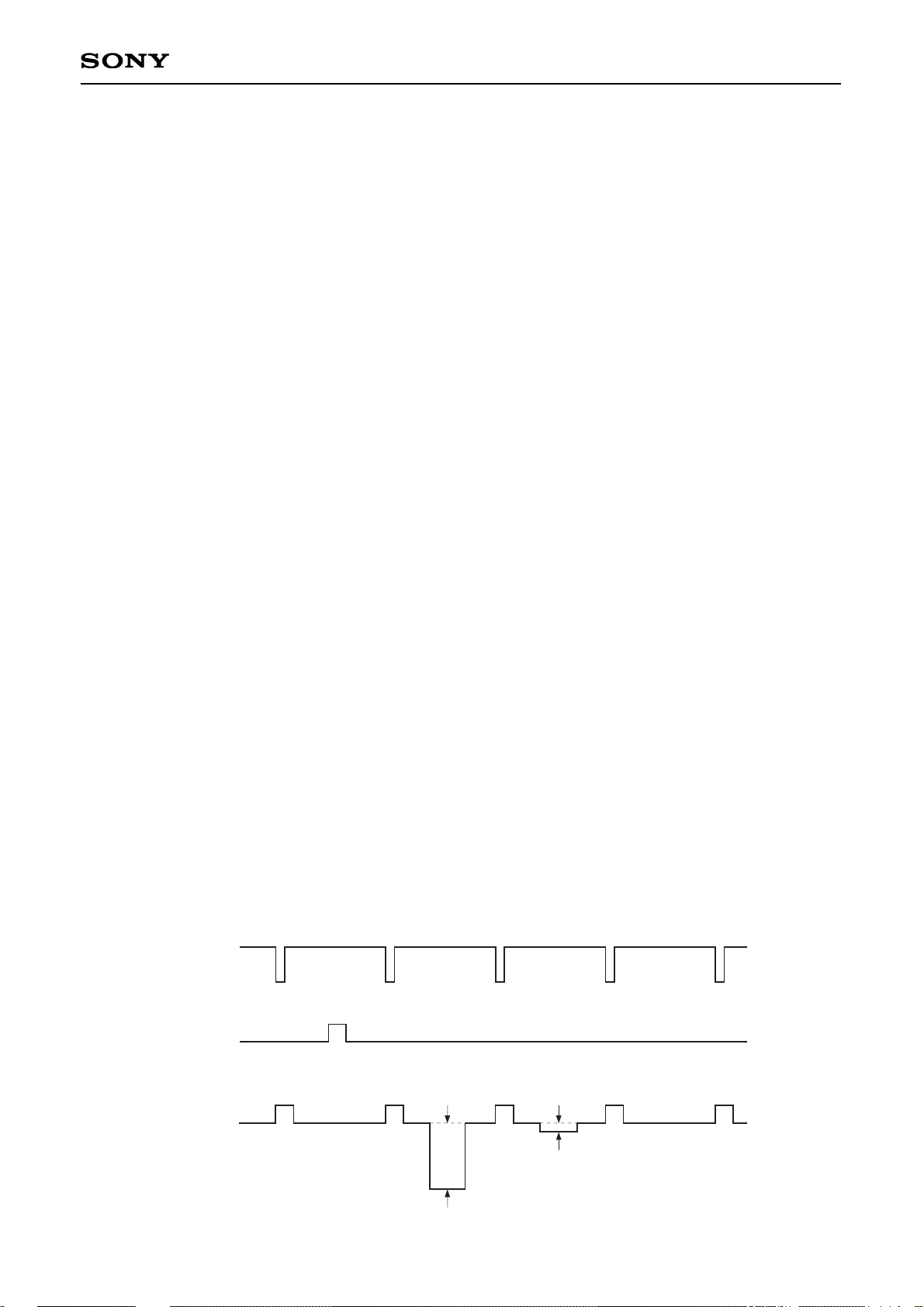
Adjust the Y signal output value generated by strobe light to 200mV. After setting the strobe light so that it
strobes with the following timing, measure the residual signal (Ylag). Substitute the value into the
following formula.
Lag = (Ylag/200) x 100 [%]
Ylag (lag)Y signal output 200mV
Light
VD
Strobe light timing
Output
Page 12
– 12 –
ICX080AK
22/16V
3.3/20V
47
1.8k
–6.5V
3.3/16V
1/35V
0.1
1M
2SK1875
CCD OUT
2200p
100k
0.1
CXD1267AN
XSUB
XV2
XV1
XSG1
XV3
XSG2
XV4
12V
22/20V
Vφ
4
Vφ
3
Vφ
2
Vφ
1
GND
GND
GND
V
OUT
Hφ
2
Hφ
1
φRG
V
L
C
SUB
φSUB
GND
V
DD
ICX080
(BOTTOM VIEW)
Hφ2
Hφ1
φRG
0.01
910111213141516
1 2 3 4 5 6 7 8
1
2
3
4
5
6
7
8
9
10
20
19
18
17
16
15
14
13
12
11
0.1
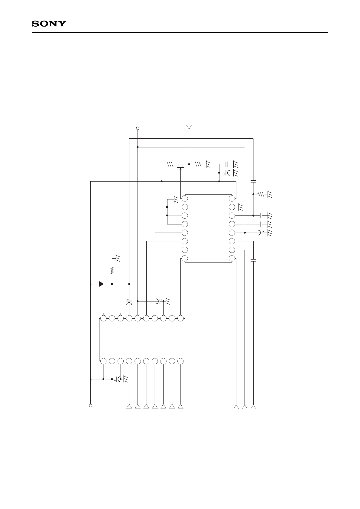
Drive Circuit
Page 13
– 13 –
ICX080AK
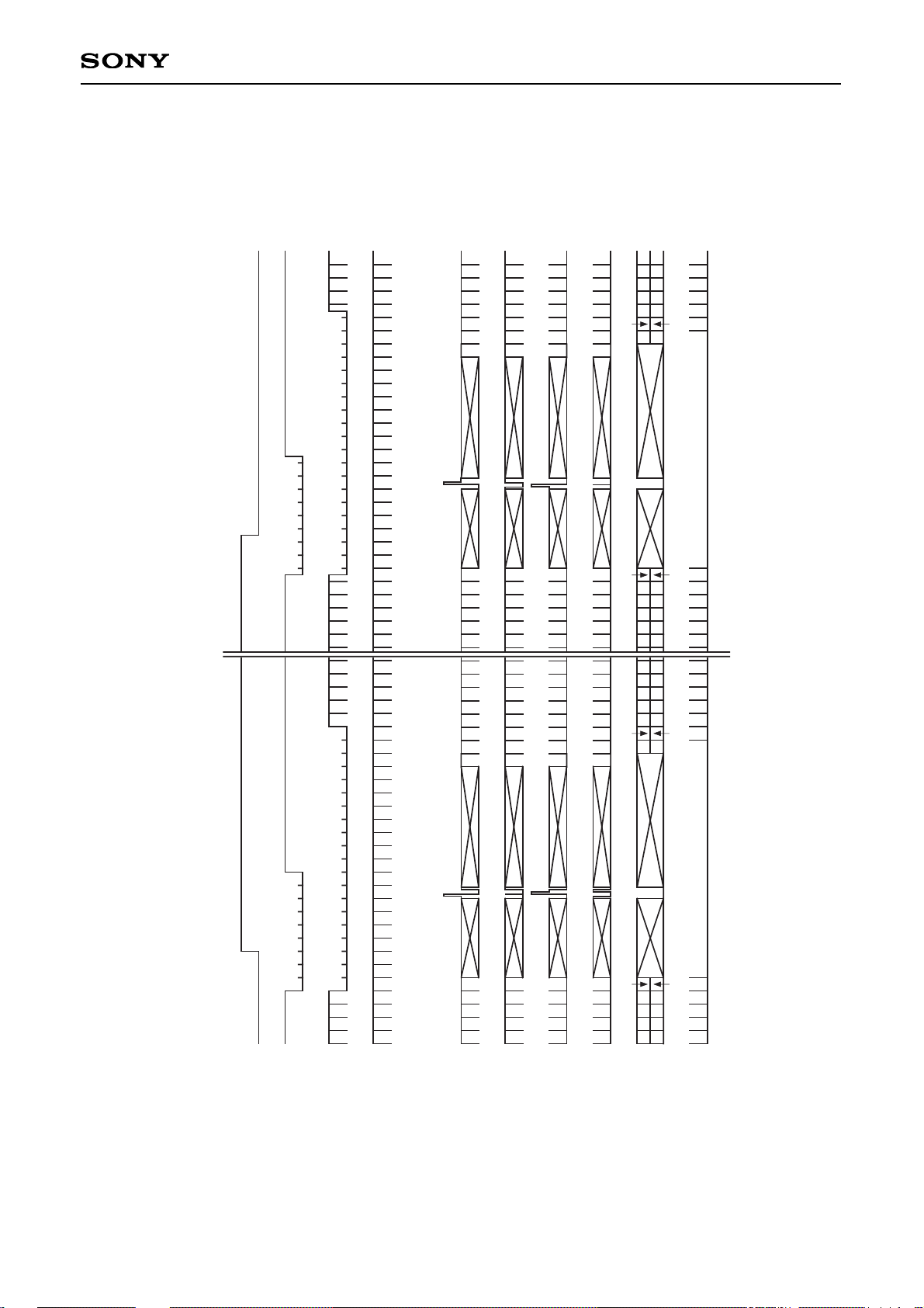
Drive Timing Chart (Vertical Sync)
HD
520
525
1
2
3
4
5
10
15
20
BLK
VD
FLD
V1
V2
V3
V4
CCD
OUT
OB
CLP
#2m + 491
#2m + 492
#2n + 4
#2n + 5
c
n + 6 stages (n = 0 to 192)
a b
246 stages
260
265
270
275
280
#2n + 490
#2n + 491
#2m + 3
#2m + 4
d
246 stages m + 6stages (m = 0 to 192)
Page 14
– 14 –
ICX080AK
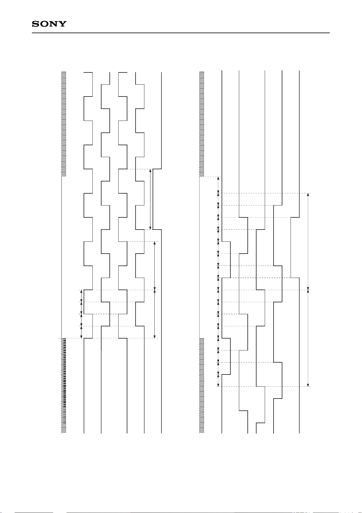
Drive Timing Chart (Vertical Sync “a” Enlarged)
V1
V2
V3
V4
7 7 7 7
#1
0
H1
#2
SUB
35
Note
H1
V1
V2
V3
V4
SUB
#n + 5
Note
#n + 6
(n = 0 to 192)
≥ 500ns
Note) Shutter pulse should be synchronized with Vφ.
7 7 7 7 7 7 7 7 7 7 7 7 7 77 7
Drive Timing Chart (Vertical Sync “c” Enlarged)
Page 15
– 15 –
ICX080AK
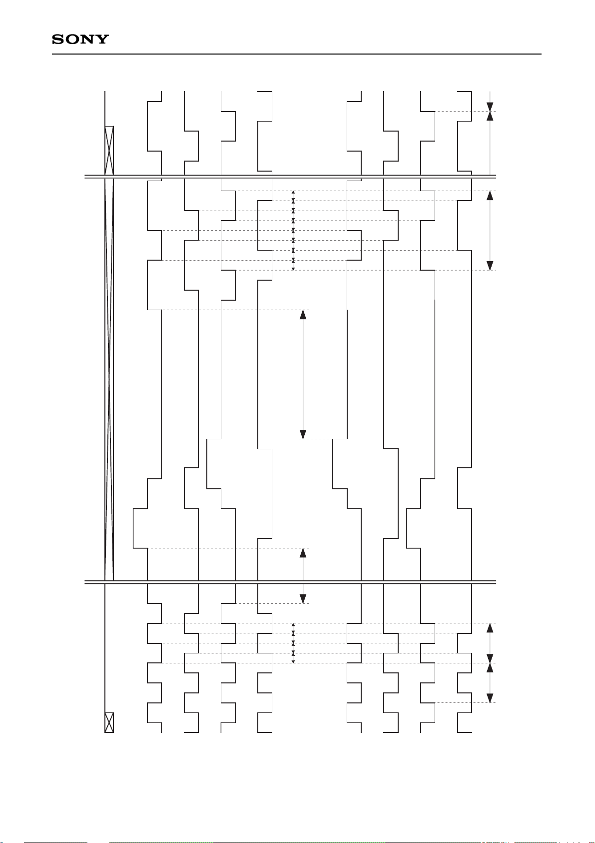
Drive Timing Chart (Vertical Sync “b” Enlarged)
H1
V1
V2
V3
V4
V1
V2
V3
V4
0
420
#1
413
203
217 252
182 245
203 231
175 203
224
378 399
357
392
350 406
364
371
385
343
7 7 7 7
#245 #246
#13
203
217 252
182 245
203 231
175 203
224
≥ 5µs≥ 5µs
7 7 7 7 7 7 7 7
427
Drive Timing Chart
(Vertical Sync “d”
Enlarged)
Page 16
– 16 –
ICX080AK
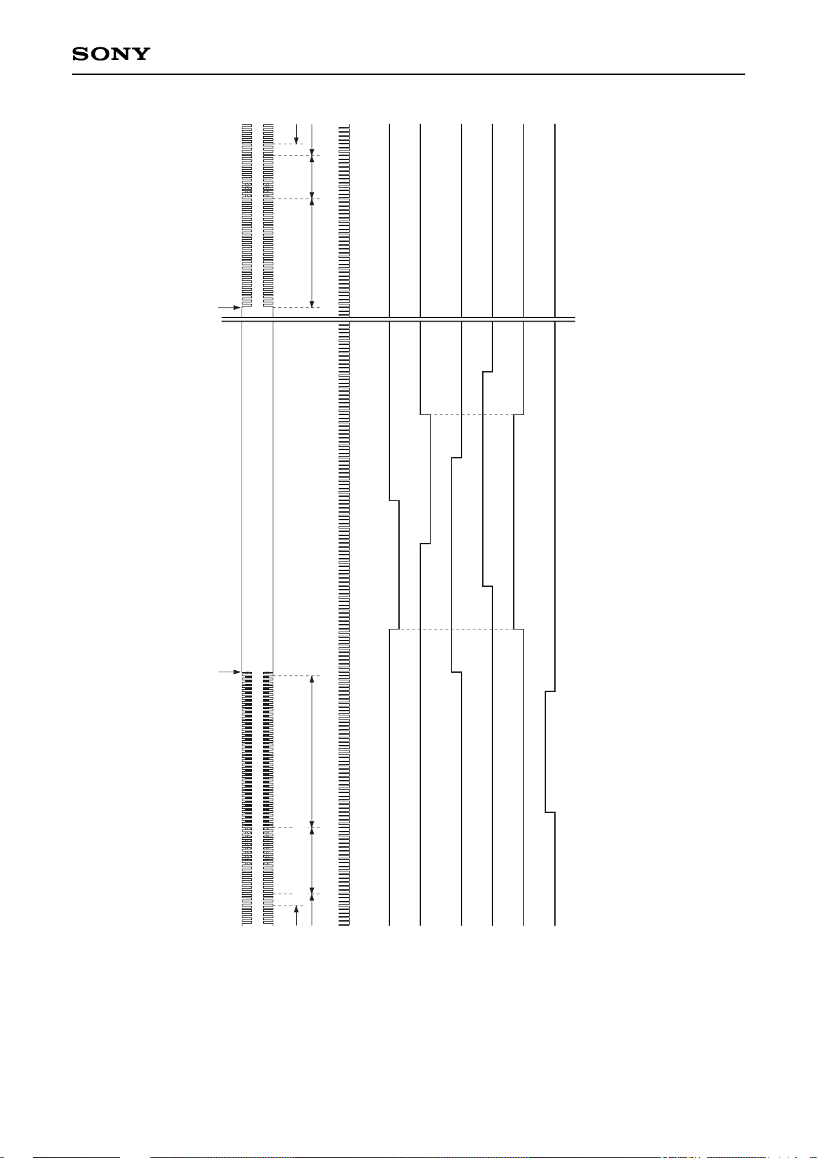
Drive Timing Chart (Horizontal Sync)
11
10
1
49
V1
V2
V3
V4
H1
H2
RG
SUB
1
11
1
8
0
0
22
33
44
77
962
28
50
55
Note) 1unit : 55.87ns (5fsc = 1137.5fh)
55.56ns (18MHz = 1144fh)
Effective region for 5fsc
955
952
Ignored region Effective OB
Ignored region
Dummy bit
–5–36
11
66
OB
CLP
Effective region for 18MHz
5fsc = 1137.5fh : 93.5
18MHz = 1144fh : 100
Page 17
– 17 –
ICX080AK
Notes on Handling
1) Static charge prevention
CCD image sensors are easily damaged by static discharge. Before handling be sure to take the following
protective measures.
a) Either handle bare handed or use non-chargeable gloves, clothes or material.
Also use conductive shoes.
b) When handling directly use an earth band.
c) Install a conductive mat on the floor or working table to prevent the generation of static electricity.
d) Ionized air is recommended for discharge when handling CCD image sensor.
e) For the shipment of mounted substrates, use boxes treated for the prevention of static charges.
2) Soldering
a) Make sure the package temperature does not exceed 80°C.
b) Solder dipping in a mounting furnace causes damage to the glass and other defects. Use a ground 30W
soldering iron and solder each pin in less than 2 seconds. For repairs and remount, cool sufficiently.
c) To dismount an image sensor, do not use a solder suction equipment. When using an electric desoldering
tool, use a thermal controller of the zero cross On/Off type and connect it to ground.
3) Dust and dirt protection
Image sensors are packed and delivered by taking care of protecting its glass plates from harmful dust and
dirt. Clean glass plates with the following operation as required, and use them.
a) Perform all assembly operations in a clean room (class 1000 or less).
b) Do not either touch glass plates by hand or have any object come in contact with glass surfaces. Should
dirt stick to a glass surface, blow it off with an air blower. (For dirt stuck through static electricity ionized
air is recommended.)
c) Clean with a cotton bud and ethyl alcohol if the grease stained. Be careful not to scratch the glass.
d) Keep in a case to protect from dust and dirt. To prevent dew condensation, preheat or precool when
moving to a room with great temperature differences.
e) When a protective tape is applied before shipping, just before use remove the tape applied for
electrostatic protection. Do not reuse the tape.
4) Installing (attaching)
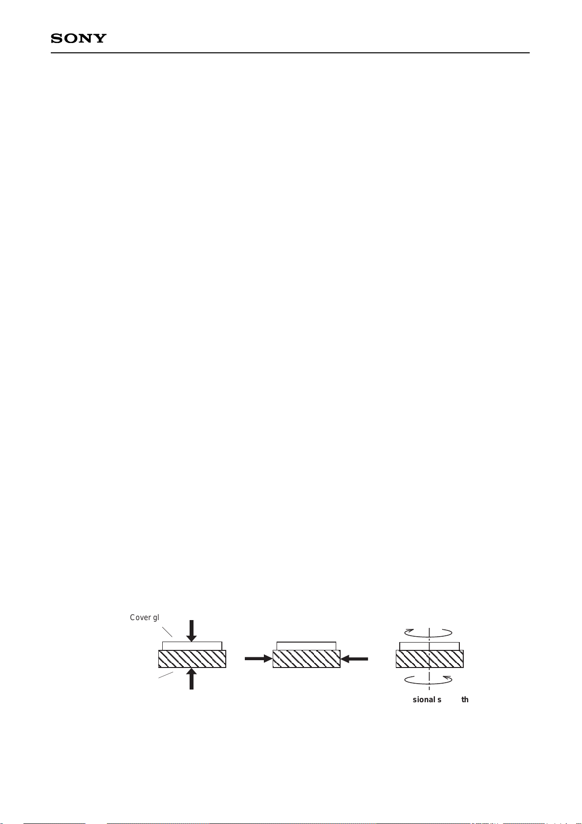
a) Remain within the following limits when applying a static load to the package. Do not apply any load more
than 0.7mm inside the outer perimeter of the glass portion, and do not apply any load or impact to limited
portions. (This may cause cracks in the package.)
b) If a load is applied to the entire surface by a hard component, bending stress may be generated and the
package may fracture, etc., depending on the flatness of the bottom of the package. Therefore, for
installation, use either an elastic load, such as a spring plate, or an adhesive.
Compressive strength
50N
Cover glass
Plastic package
50N
1.2Nm
Torsional strength
Page 18

– 18 –
ICX080AK
c) The adhesive may cause the marking on the rear surface to disappear, especially in case the regulated
voltage value is indicated on the rear surface. Therefore, the adhesive should not be applied to this area,
and indicated values should be transferred to the other locations as a precaution.
d) The notch of the package is used for directional index, and that can not be used for reference of fixing.
In addition, the cover glass and seal resin may overlap with the notch of the package.
e) If the lead bend repeatedly and the metal, etc., clash or rub against the package, the dust may be
generated by the fragments of resin.
f) Acrylate anaerobic adhesives are generally used to attach CCD image sensors. In addition, cyano-
acrylate instantaneous adhesives are sometimes used jointly with acrylate anaerobic adhesives. (reference)
5) Others
a) Do not expose to strong light (sun rays) for long periods, color filters will be discolored. When high
luminance objects are imaged with the exposure level control by electronic-iris, the luminance of the
image-plane may become excessive and discolor of the color filter will possibly be accelerated. In such a
case, it is advisable that taking-lens with the automatic-iris and closing of the shutter during the power-off
mode should be properly arranged. For continuous using under cruel condition exceeding the normal
using condition, consult our company.
b) Exposure to high temperature or humidity will affect the characteristics. Accordingly avoid storage or
usage in such conditions.
c) The brown stain may be seen on the bottom or side of the package. But this does not affect the CCD
characteristics.
Page 19
– 19 –
ICX080AK
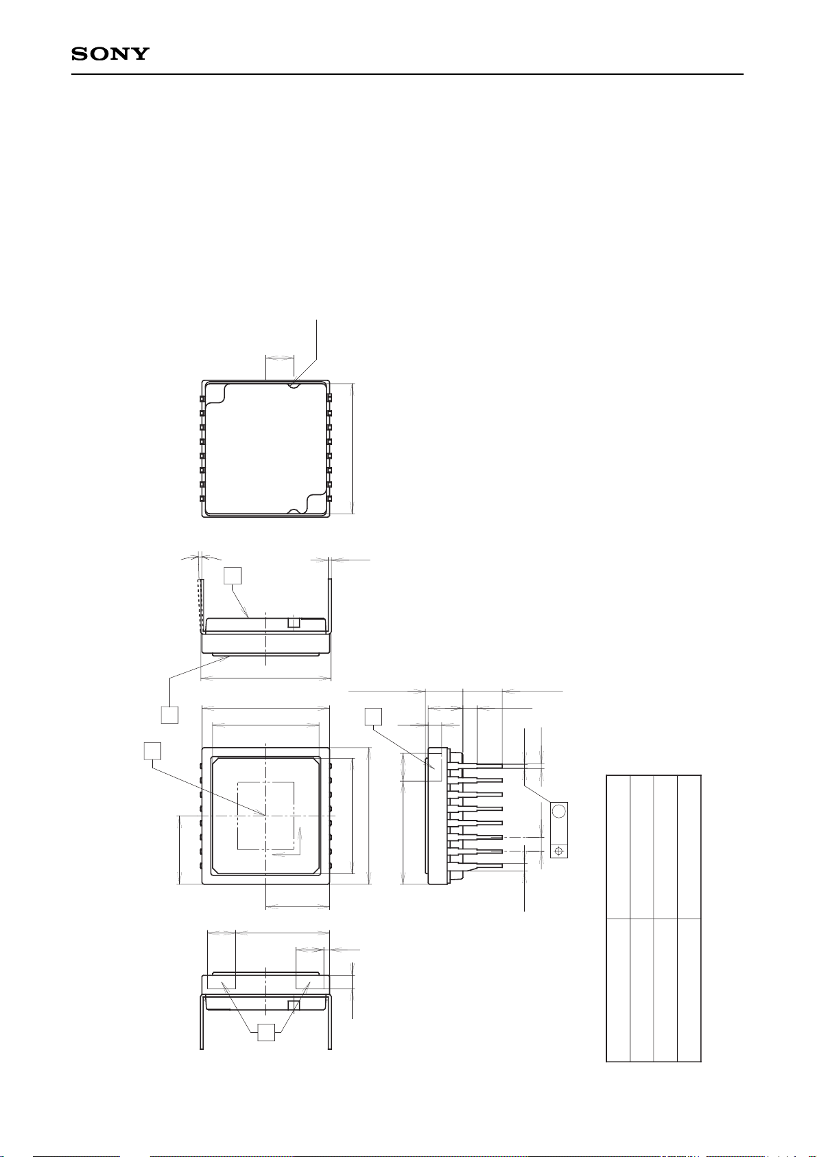
PACKAGE STRUCTURE
0.3
16pin DIP (450mil)
H
V
2.5
2.5
8.4
0.5
1.2
5.7
6.1
10.3
12.2 ± 0.1
9.5
11.4 ± 0.1
11.43
0.25
0° to 9°
8
1
16
9
2-R0.5
2.5
11.6
9.2
2.5
1.2
3.35 ± 0.15
3.1
1.27
3.5 ± 0.3
0.46
0.3
1.27
0.69
(For the first pin only)
1. “A” is the center of the effective image area.
2. The two points “B” of the package are the horizontal reference.
The point “B'” of the package is the vertical reference.
3. The bottom “C” of the package, and the top of the cover glass “D”
are the height reference.
4. The center of the effective image area relative to “B” and “B'”
is (H, V) = (6.1, 5.7) ± 0.15mm.
5. The rotation angle of the effective image area relative to H and V is ± 1°.
6. The height from the bottom “C” to the effective image area is 1.41 ± 0.10mm.
The height from the top of the cover glass “D” to the effective image area is 1.94 ± 0.15mm.
7. The tilt of the effective image area relative to the bottom “C” is less than 50µm.
The tilt of the effective image area relative to the top “D” of the cover glass is less than 50µm.
8. The thickness of the cover glass is 0.75mm, and the refractive index is 1.5.
9. The notches on the bottom of the package are used only for directional index, they must
not be used for reference of fixing.
C
B
A
D
M
B'
~
~
~
PACKAGE MATERIAL
LEAD TREATMENT
LEAD MATERIAL
PACKAGE WEIGHT
Plastic
GOLD PLATING
42 ALLOY
0.9g
Package Outline Unit: mm
 Loading...