

Page 1
TL/DD11727
ICSS1001, ICSS1002, and ICSS1003 IC/SS Power Line Carrier Local Area Network Chip Set
PRELIMINARY
February 1995
ICSS1001, ICSS1002, and ICSS1003
IC/SS Power Line Carrier
Local Area Network Chip Set
General Description
Integrated Circuit/Spread Spectrum (IC/SSTM) is a power
line carrier local area network system implemented in a
three chip solution, using power line carrier technology developed by Itron and Cyplex. It is designed to operate with
high reliability over the full range of power line conditions.
IC/SS is offered with an integral local area network protocol, designed specifically for supervisory control and data
acquisition applications.
Features
Y
Spread spectrum, adaptive frequency hopping modulation provides high immunity to power line noise.
Y
Network/transparent option offers the user the ability to
carry proprietary protocols transparently, or to use the
built-in link layer protocol.
Y
A very flexible interface to the user’s circuit is provided,
configurable either to accept serial data or to accept
data from an 8-bit parallel bus. Handshake lines are
provided to facilitate interface to common microprocessors in parallel mode.
Y
When used with the specified coupling networks, the
modem operates in conformance with both the
CENELEC standard for electric utility application
(9 kHz–95 kHz), and with FCC Class A requirements.
Y
Data rate is variable, based on line conditions, from
300 bps to 3200 bps.
Y
When used with the specified coupling networks, the
system provides 93 dB of dynamic range, appropriate
for line loading and attenuation effects common on
power lines.
Y
The modem’s bit error rate performance in additive
white noise approaches the theoretical maximum, and
in addition it provides excellent immunity to the impulsive noise characteristic of power lines.
Applications
Y
Automated meter reading (AMR)
Y
Demand side management
Y
Distribution automation
Y
Environmental control systems
Y
Other power line carrier applications requiring high
reliability
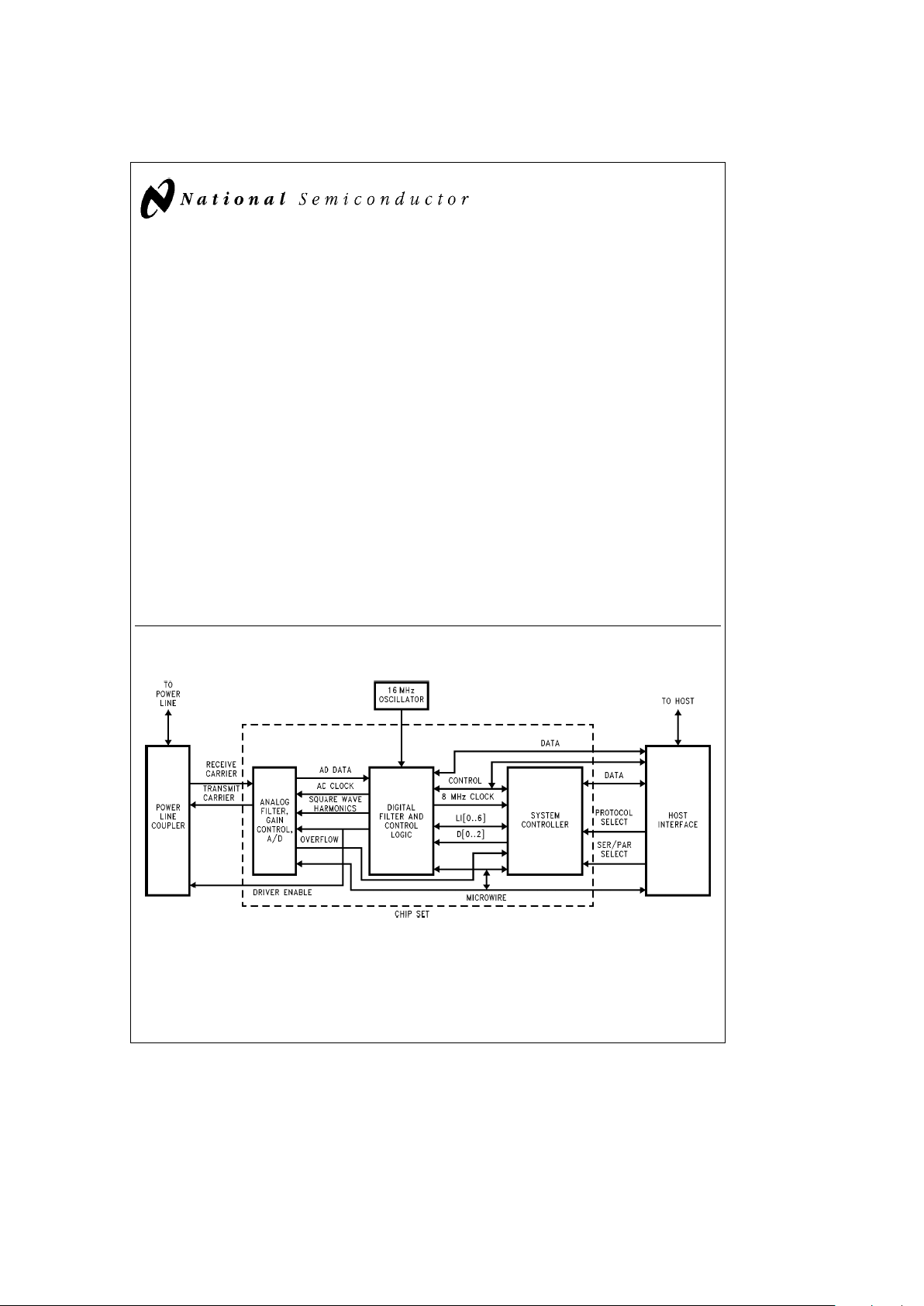
Block Diagram
TL/DD/11727– 1
TRI-STATEÉis a registered trademark of National Semiconductor Corporation.
MICROWIRE
TM
and WATCHDOGTMare trademarks of National Semiconductor Corporation.
IC/SS
TM
is a trademark of Cyplex.
C
1995 National Semiconductor Corporation RRD-B30M105/Printed in U. S. A.
Page 2
Modem Operation
A block diagram of the modem is shown on page 1. It includes four major elements:
1. Coupling network to the power line.
2. Analog filter, gain control, and A/D.
3. Digital filter and control logic.
4. System controller.
Each of these is described in more detail below.
COUPLING NETWORK
The coupling network provides protection against the AC
power line 60 Hz/50 Hz energy, and initial filtering of power
line noise. It provides a match of impedances to the power
line, and also contains a power amplification stage for the
transmitter. A variety of coupling networks are available
from Cyplex, suitable for:
220 VAC ungrounded operation (meters and 220 VAC
load control).
110 VAC/neutral operation (110 VAC load control).
Three-terminal operation (intended for gateways and
master units which must communicate with both of the
above).
The coupling networks require
g
5V power, ground, and in-
terface to the analog section of the system.
ICSS1001ÐController
The controller provides the adaptive frequency hopping, the
user interface, and link layer protocol.
ICSS1002ÐDigital Chip
The digital section of the system provides additional receive
filtering and received signal detection functions. It generates
the necessary internal clocks and interface signals to the
microcontroller.
ICSS1003ÐAnalog Chip
The analog section of the system provides receive signal
filtering, and also generates the transmit carrier based on
control and clock signals from the digital section.
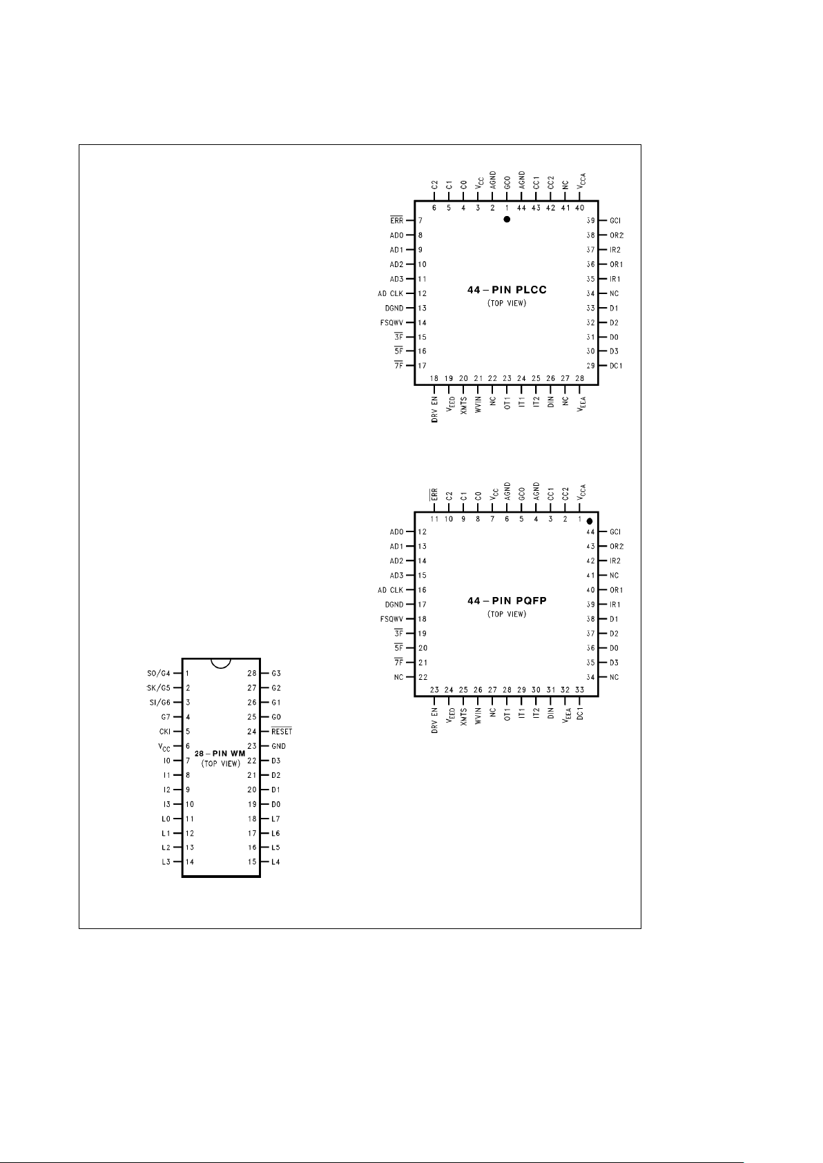
Connection Diagrams
TL/DD/11727– 2
Wide Molded Small Outline Package (WM)
Order Number ICSS1001WM
NS Package Number M28B
TL/DD/11727– 4
Plastic Leaded Chip Carrier (PLCC)
Order Number ICSS1003V
NS Package Number V44A
TL/DD/11727– 28
Plastic Quad Flatpak (PQFP)
Order Number ICSS1003VGZ
NS Package Number VGZ44A
2
Page 3
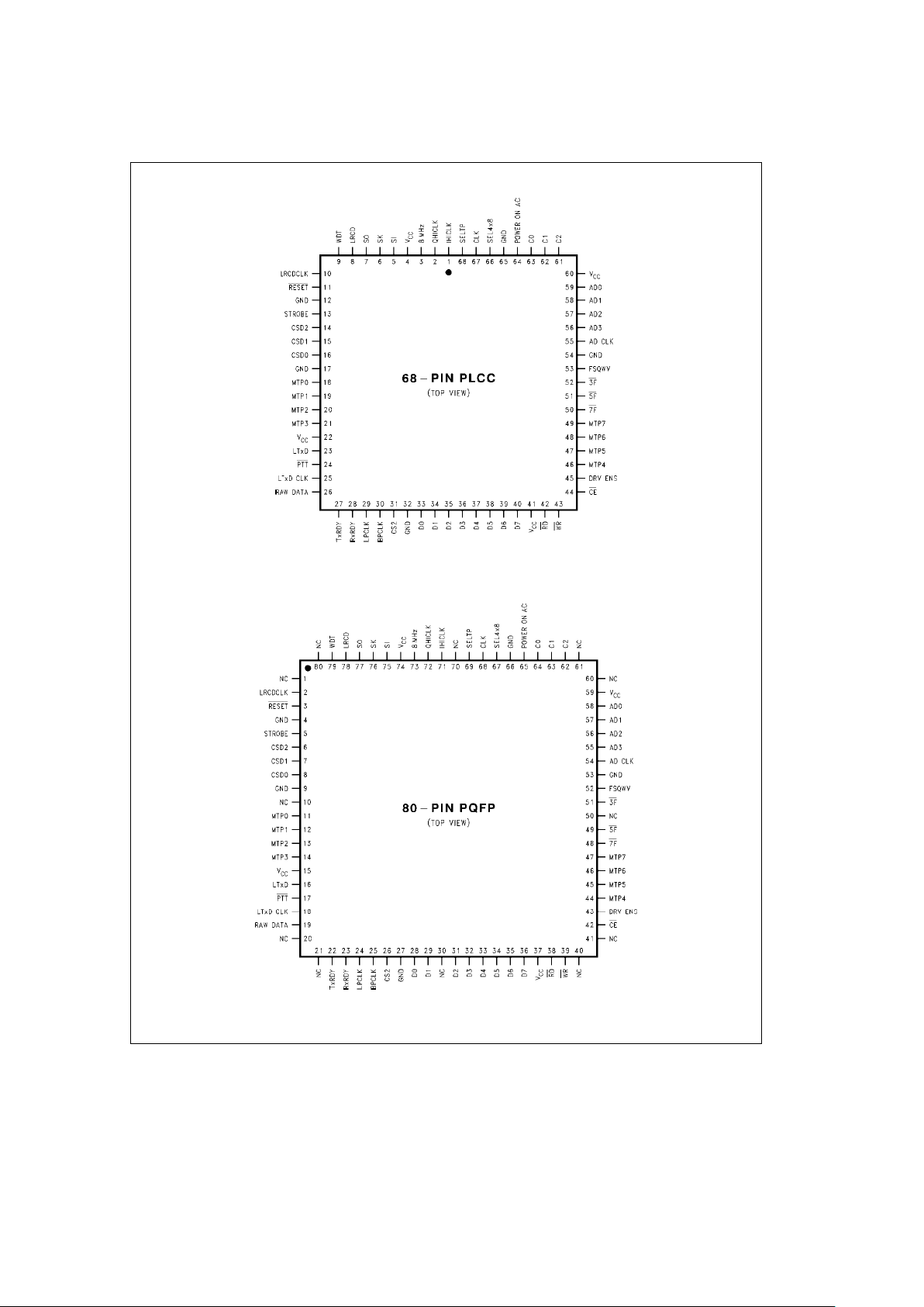
Connection Diagrams (Continued)
TL/DD/11727– 3
Plastic Leaded Chip Carrier (PLCC)
Order Number ICSS1002V4
NS Package Number V68A
TL/DD/11727– 27
Plastic Quad Flatpak (PQFP)
Order Number ICSS1002VJE
NS Package Number VJE80B
3
Page 4
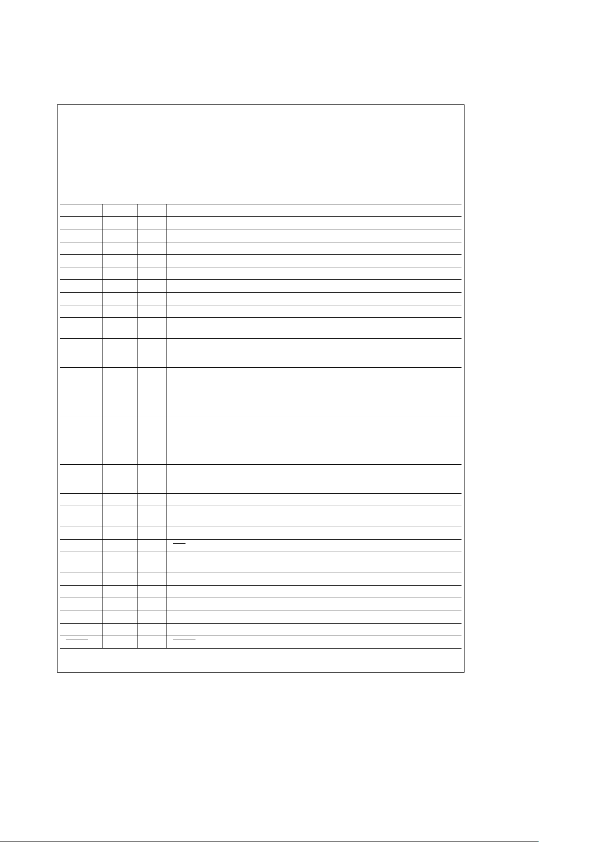
Pin Descriptions
Tables I, II and III describe the various pins that are used for
external connections outside of the chip set. These pins are
shown in the Connection Diagrams.
Type One of the following:
I Input
O Output
T TRI-STATE
É
P Power
Function A brief description of each signal’s function.
TABLE I. ICSS1001 Pin Descriptions
Pin Name Pin No. Type Function
SO/G4 1 O MICROWIRETMSO to digital ASIC
SK/G5 2 O MICROWIRE clock to digital ASIC
SI/G6 3 I MICROWIRE SI from digital ASIC
G7 4 O Overflow of A/D converter from analog ASIC
CKI 5 l 8 MHz clock input from digital ASIC
V
CC
6 P Input power
I0 7 I RAW DATA input from digital ASIC
I1 8 O RxRDY handshake line for parallel port
I2 9 I SER/PAR-input read after reset determines whether firmware will use serial or parallel host
port. HIGH
e
serial
I3 10 I NET/TRN-input read continuously. If HIGH and serial port is selected commands are
processed; if LOW, all received characters are treated as transparent data. If parallel port is
selected, this pin has no effect.
L0 11 I RTS flow control from host. If serial port is selected (pin 9eHIGH), LOW enables output of
data on RCD and HIGH prevents output on RCD. A byte in the process of being output when
RTS goes HIGH will be completed. RTS has no effect if parallel port is selected.
If parallel is selected (pin 9
e
LOW), COMMAND HIGH denotes the presence of a command
in the parallel port input buffer. LOW denotes the presence of data.
L1 12 O CTS flow control to host. Normally LOW. If serial port is selected (pin 9eHIGH) then HIGH
indicates host should not send data to TXD. A maximum of three bytes will be accepted after a
transition from LOW to HIGH.
If parallel port is selected (pin 9
e
LOW), then STATUS HIGH denotes that the byte available
for the host to read is a status code. A LOW denotes that the available byte is data.
L2 13 O RCD receive data output to host, in byte asynchronous format, 8 data bits, parity one start and
one stop bit. Active baud rate and parity default is 1200 baud, no parity. Other settings may be
selected by DIP switch. Active only if serial port is selected.
L3 14 I TXD transmit data input from host
L4 15 O LTXD CLK serial data clock for data to be transmitted by the digital ASIC, not Manchester-
encoded
L5 16 O TxRDY handshake line for parallel port
L6 17 O PTT Active LOW places digital chip in transmit mode
L7 18 O LTXD serial data to be transmitted by digital ASIC, not Manchester-encoded. Active HIGH.
ASIC Manchester-encodes the data using LTXD CLK.
D0 19 O CSD digital ASIC internal MlCROWIRE register address selection
D1 20 O CSD1 digital ASIC internal MlCROWIRE register address selection
D2 21 O CSD2 digital ASIC internal MICROWIRE register address selection
D3 22 O STROBE MICROWIRE output to digital ASIC
GROUND 23 P Ground
RESET 24 I RESET from digital chip
4
Page 5
Pin Descriptions (Continued)
TABLE I. ICSS1001 Pin Descriptions (Continued)
Pin Name Pin No. Type Function
G0 25 I LRCD CLK recovered clock from demodulated data input from digital ASlC
G1 26 No connection
G2 27 I LRCD recovered data from demodulated data input from digital ASIC, after Manchester
decoding
G3 28 O WDT firmware outputs a square wave to digital chip, maintaining a one-shot. If WDT output
stops, digital ASIC will force a system reset on pin 24.
TABLE II. ICSS1002 Pin Descriptions
Pin Name
Pin No.
Type Function
(V Pkg.)
IHICLK 1 O Output Test Point: A test point.
QHICLK 2 O Output Test Point: A test point.
8 MHz 3 O 8 MHz Output: This is the CLK divided by 2. This output goes low while RESET is LOW.
SI 5 T MICROWIRE Serial Input: This pin drives the MICROWIRE SI Input on the controller.
SK 6 T MICROWIRE Shift Clock: This pin accepts the MICROWIRE shift clock to the Controller
interface on the IC/SS digital ASIC.
SO 7 T MICROWIRE Serial Output: This pin accepts the MICROWIRE serial data to the
Controller interface on the IC/SS digital ASIC.
LRCD 8 O Recovered Data: This is the serial data received from the power line after Manchester
decoding.
WDT 9 T WATCHDOGTMTimer Disable: This input from the controller keeps the digital ASIC
active. If it goes away, the digital ASlC will generate RESET
pulse after the WATCHDOG
timers times out. This RESET
pulse will reset the entire PLC chip set.
LRCDCLK 10 O Recovered Clock: This is the clock received from the power line after Manchester
decoding.
RESET 11 I Reset: Active LOW reset for the entire IC/SS chip set.
STROBE 13 T MICROWIRE Strobe input: This pin accepts the MICROWIRE strobe to the controller
interface on the IC/SS digital ASIC.
CSD2–CSD0 14–16 T Controller Interface Mode Select: These inputs are used to select the operation modes
of the controller interface circuitry on the IC/SS digital ASIC.
MTP0–MTP3 18– 21 O Test Points: These output pins provide access to one of the filter outputs on the detector
integration bus.
LTXD 23 O Serial Data to be transmitted: This input is the serial data to be transmitted. It is not
Manchester encoded.
PTT 24 T Push to talk: This is an active low signal that puts the digital ASIC into the transmit mode.
LTXD CLK 25 T Serial Data Transmit Clock: This input is the clock for the serial data (LTXD) that is used
to Manchester encode the data prior to transmission.
RAW DATA 26 O Raw Data: This output is the raw data received by the IC/SS circuit after de-multiplex prior
to Manchester decode.
TxRDY 27 O Transmit Data Ready: When this signal is HIGH the parallel port is ready to accept a new
byte from the user data bus.
RxRDY 28 O Receive Data Ready: When this signal is HIGH there is a byte available in the parallel
port to be read by the user data bus.
LPCLK 29 O LPCLK: This is an internal test point.
BPCLK 30 O BPCLK: This is an internal test point.
CS2 31 O Chip Select: This is the MICROWIRE chip select output. It is used to enable read/write of
external MICROWIRE data ports.
5
Page 6
Pin Descriptions (Continued)
TABLE II. ICSS1002 Pin Descriptions (Continued)
Pin Name
Pin No
Type Function
(V Pkg.)
D0–D7 33–40 I/O Data Bus: This is the parallel port data bus.
RD 42 T Read: This is the parallel port read control. Used with Chip Enable it allows the
parallel port to be read.
WR 43 T Write: This is the parallel port write control. Used with Chip Enable it allows the
parallel port to be written.
CE 44 T Chip Enable: This is the parallel port enable to read or write. It is active low.
DRV EN 45 O Drive Enable: This is the transmit enable signal used by the Analog chip to disable
the receiver mode and enable the transmitter mode
MTP4–MTP7 46–49 O Test Points: These output pins provide access to one of the filter outputs of the
detector integration bus
7F 50 O Seventh Harmonic Overtone Cancellation Signal: This is the seventh harmonic
overtone cancellation signal used to convert FSQWV to a sine wave in the Analog
chip D/A
5F 51 O Fifth Harmonic Overtone Cancellation Signal: This is the fifth harmonic overtone
cancellation signal used to convert FSQWV to a sine wave in the Analog chip D/A
3F 52 O Third Harmonic Overtone Cancellation Signal: This is the Third harmonic overtone
cancellation signal used to convert FSQWV to a sine wave in the Analog chip D/A
FSQWV 53 O Square Wave Transmit Signal: This is the Manchester-encoded frequency mixed
signal, ready for transmission to the power line
AD CLK 55 O A/D Clock: This is the clock for the Analog chip AID converter. It is used to latch the
AD output. It is the A/D sample rate. This is the CLK divided by 16. This output goes
HIGH while RESET
is LOW.
AD3–AD0 56 – 59 T Received Data: These pins are the digital four bit bus from the Analog chip which
contains the ones complement A/D converted signal from the power line
C2–C0 61–63 O Analog Gain Control: These signals are used to set the gain of the Analog chip gain
controlled amplifier
Power on AC 64 O Power on Reset RC Node: This is the power on reset Resistor/Capacitor connect
point. An external RC network charges up to the gate threshold to release the RESET
signal. When this pin is LOW the RESET is active.
SEL4X8 66 T Select 4X or 8X: This is the select line used to set the digital filter clock sample rate
CLK 67 T Clock: This is the 16 MHz clock input
SEL TP 68 T Select Test Points: This signal selects which internal nodes are brought out on the
Test Point Bus and whether Raw Data is inverted or not
V
CC
4, 22, 41, 60 P VCC: These are positive voltage power supply pins to the part
GND 12, 17, 32, P GND: These are the negative (or 0V) power supply pins to the part
54, 65
TABLE III. ICSS1003 Pin Descriptions
Pin Name
Pin No.
Type Function
(V Pkg.)
GCO 1 Gain Control Amplifier Test Point: A test point to monitor the gain of the gain amplifier
AGND 2 P Analog Ground: The ground reference pin for the gain control amplifier
V
CC
3PDigital Positive Power Supply Pin: The VCCpin for the digital portion of the ASIC
C0–C2 4–6 I Gain Control Amplifier Gain Setting: These pins set the gain of the gain control amplifier.
These signals are generated by the digital ASIC.
ERR 7OA/D Overflow Signal: This signal goes HIGH if the Analog signal from the gain control
amplifier to the Analog to Digital Converter is being clipped by the A/D converter
6
Page 7
Pin Descriptions (Continued)
TABLE III. ICSS1003 Pin Descriptions (Continued)
Pin Name
Pin No.
Type Function
(V Pkg.)
AD0–AD3 8 – 11 O A/D Digital Output: These signals are the ones complement digital output of the signal
received from the power line. It is the output of the flash A/D sampled at the AD CLK rate.
AD CLK 12 I Clock For The Flash A/D Converter: This is the clock used by the A/D converter to sample
the signal received from the power line. It is normally 1 MHz and is generated by the digital
ASIC.
DGND 13 P Digital Ground Power Supply Pin: This is the ground (0V) power supply for the digital
portion of the ASIC
FSQWV 14 I Square Wave Transmit Signal: This is the Manchester-encoded, frequency mixed signal
3F 15 I Third Harmonic Overtone Cancellation Signal: This is the third harmonic overtone
cancellation signal used to convert FSQWV to a sine wave in the Analog chip D/A
5F 16 I Fifth Harmonic: Overtone Cancellation Signal: This is the fifth harmonic overtone
cancellation signal used to convert FSQWV to a sine wave in the Analog chip D/A
7F 17 I Seventh Harmonic: Overtone Cancellation Signal: This is the seventh harmonic overtone
cancellation signal used to convert FSQWV to a sine wave in the Analog chip D/A
DRV EN 18 I Drive Enable: This is the transmit enable signal used by the Analog chip to disable the
receiver mode and enable the transmitter mode
VEED 19 P Digital Negative Power Supply Pin: This is the negative (b5V) power supply for the digital
portion of the ASIC
XMTS 20 O Digital To Analog Converter Integrator Output: This is the analog output of the D/A
converter integrator
WVIN 21 Digital To Analog Converter Integrator Input: This is the analog input of the D/A converter
integrator. It is connected internally to the D/A converter output. It is used to connect the
external integrator capacitor to the integrator input.
OT1 23 O Amplifier Output: Buffer amplifier between the D/A converter and the power driver amplifier
output
IT1 24 I Amplifier Positive Input: Buffer amplifier between the D/A converter and the power driver
amplifier positive input
IT2 25 I Amplifier Negative Input: Buffer amplifier between the D/A converter and the power driver
amplifier negative input
DIN 26 I Power Amplifier Input: This is the power amplifier input
VEEA 28 P Analog Negative Power Supply Pin: This is the negative (b5V) power supply for the analog
portion of the ASIC
DC1 29 O Power Amplifier Divided Input: This is the power amplifier resistor divided input
D3 30 I Power Amplifier Feedback Input: This is one of the switched power amplifier feedback
points
D0 31 I Power Amplifier Feedback Input: This is one of the switched power amplifier feedback
points
D2 32 O Power Amplifier Negative Output: This is the power amplifier negative output driver output
D1 33 O Power Amplifier Positive Output: This is the power amplifier positive output driver output
IR1 35 O Unity Gain Amplifier Input: First stage receiver filter input
OR1 36 O Unity Gain Amplifier Output: First stage receiver filter output
IR2 37 I Unity Gain Amplifier Input: Second stage receiver filter input
7
Page 8
Pin Descriptions (Continued)
TABLE III. ICSS1003 Pin Descriptions (Continued)
Pin Name
Pin No.
Type Function
(V Pkg.)
IR2 38 O Unity Gain Amplifier Output: Second stage receiver filter output
GCI 39 I Gain Control Amplifier Input: This is the gain control amplifier input
VCCA40PAnalog Positive Power Supply Pin: The VCCpin for the analog portion of the ASIC
CC2 42 Gain Control Amplifier Offset Compensation Input: This is the gain control amplifier
offset compensation input capacitor connect point
CC1 43 Gain Control Amplifier Offset Compensation Output: This is the gain control
amplifier offset compensation output capacitor connect point
AGND 44 Analog Gain Control: This is the ground (0V) power supply for the analog portion of the
ASIC
NC 22, 27, 34, 41 No Connect: These pins are not connected
Absolute Maximum Ratings
If Military/Aerospace specified devices are required,
please contact the National Semiconductor Sales
Office/Distributors for availability and specifications.
Supply Voltage 7V
Total Current into V
CC
Pin (Source) 100 mA
Total Current out of GND Pin (Sink) 110 mA
Storage Temperature Range
b
65§Ctoa150§C
Note:
Absolute maximum ratings indicate limits beyond
which damage to the device may occur. DC and AC electrical specifications are not ensured when operating the device at absolute maximum ratings.
ICSS1001 DC Electrical Characteristics (
b
40§CsT
A
s
a
85§C)
Parameter Conditions Min Typ Max Units
Operating Voltage Power Supply Ripple (Note 1) 2.5 5.5
V
Peak to Peak 0.1 V
CC
Supply Current
CKI
e
10 MHz (Note 2) V
CC
e
6V, t
C
e
1 ms15
mA
CKI
e
4 MHz V
CC
e
2.5V, t
C
e
2.5 ms2
HALT (Note 3) V
CC
e
6V, CKIe0 MHz
k
110mA
IDLE
CKI
e
10 MHz V
CC
e
6V, t
C
e
1 ms 2.2 mA
CKI
e
4 MHz V
CC
e
2.5V, t
C
e
2.5 ms 0.6 mA
Input Levels (VIH,VIL)
Reset, CKI
V
Logic HIGH 0.8 V
CC
Logic LOW 0.2 V
CC
All Other Inputs
Logic HIGH 0.7 V
CC
Logic LOW 0.2 V
CC
Hi-Z Input Leakage Input Pull-Up Current V
CC
e
6V
b
2
a
2
mA
V
CC
e
6V, V
IN
e
0V 40 250
G Port Input Hysteresis (Note 6) 0.05 V
CC
0.35 V
CC
V
8
Page 9
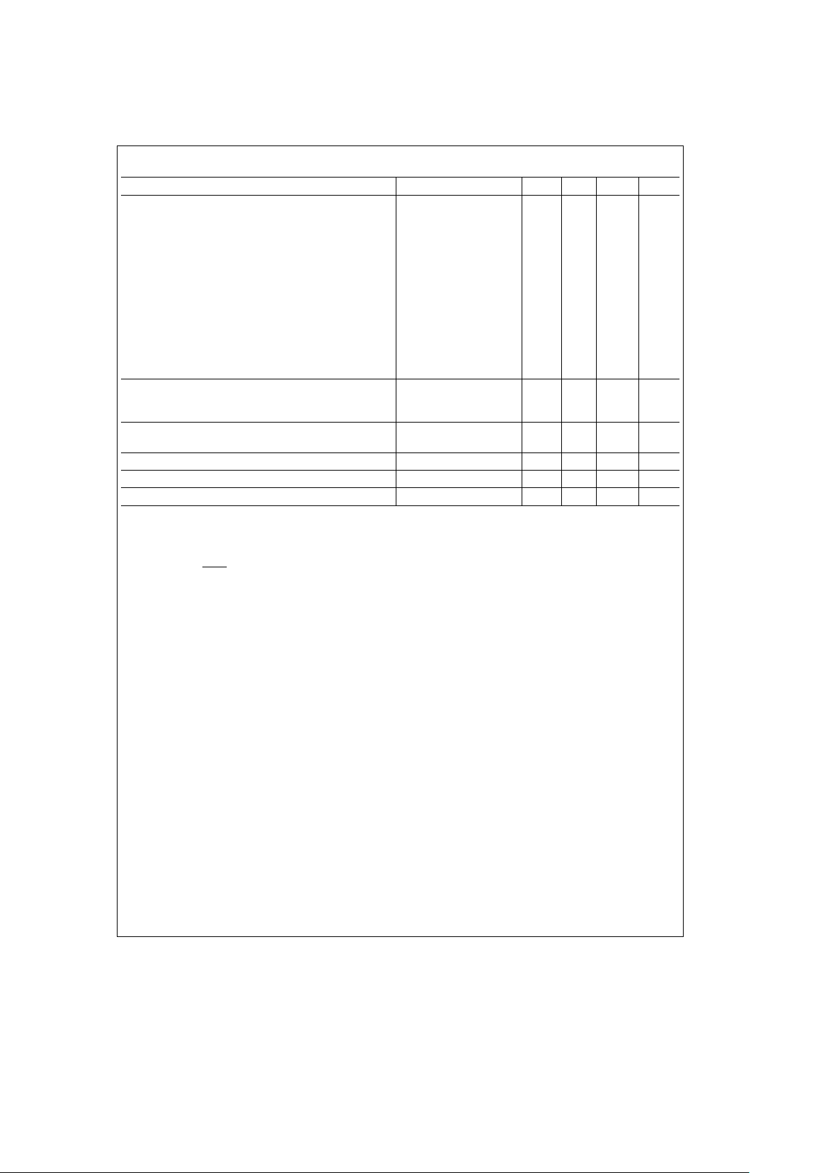
ICSS1001 DC Electrical Characteristics (
b
40§CsT
A
s
a
85§C) (Continued)
Parameter Conditions Min Typ Max Units
Output Current Levels
D Outputs
Source V
CC
e
4.0V, V
OH
e
3.3V 0.4 mA
V
CC
e
2.5V, V
OH
e
1.8V 0.2 mA
Sink V
CC
e
4.0V, V
OL
e
1.0V 10 mA
V
CC
e
2.5V, V
OL
e
0.4V 0.2 mA
All Others
Source (Weak Pull-Up) V
CC
e
4.0V, V
OH
e
2.7V 10 110 mA
V
CC
e
2.5V, V
OH
e
1.8V 2.5 33 mA
Source (Push-Pull) V
CC
e
4.0V, V
OH
e
3.3V 0.4 mA
V
CC
e
2.5V, V
OH
e
1.8V 0.2 mA
Sink (Push-Pull) V
CC
e
4.0V, V
OL
e
0.4V 1.6 mA
V
CC
e
2.5V, V
OL
e
0.4V 0.7 mA
TRI-STATE Leakage V
CC
e
6.0V
b
2.0
a
2.0 mA
Allowable Sink/Source Current per Pin
D Outputs (Sink) 15
mA
All Other 3
Maximum Input Current without Latchup Room Temp
g
100 mA
(Notes 4, 6)
RAM Retention Voltage, VR(Note 5) 500 ns Rise and Fall Time 2.0 V
Input Capacitance (Note 6) 7 pF
Load Capacitance (Note 6) 1000 pF
Note 1: Maximum rate of voltage change must be less than 0.5V/ms.
Note 2: Supply current is measured after running 2000 cycles with a square wave CKI input, CKO open, inputs at rails, and outputs open.
Note 3: The HALT mode will stop CKI from oscillating in the RC and the Crystal configurations. HALT test conditions: all inputs tied to V
CC
; L and G port I/Os
configured as outputs and programmed low; D outputs programmed low. Parameter refers to HALT mode entered via setting bit 7 of the G Port data register. Part
will pull up CKI during HALT in crystal clock mode.
Note 4: Pins G6 and RESET
are designed with a high voltage input network. These pins allow input voltages greater than VCCand the pins will have sink current to
V
CC
when biased at voltages greater than VCC(the pins do not have source current when biased at a voltage below VCC). The effective resistance to VCCis 750X
(typical). These two pins will not latch up. The voltage at the pins must be limited to less than 14V. Voltages in excess of 14V will cause damage to the pins. This
excludes ESD transients.
Note 5: Condition and parameter valid only for part in HALT mode.
Note 6: Parameter characterized but not tested.
9
Page 10
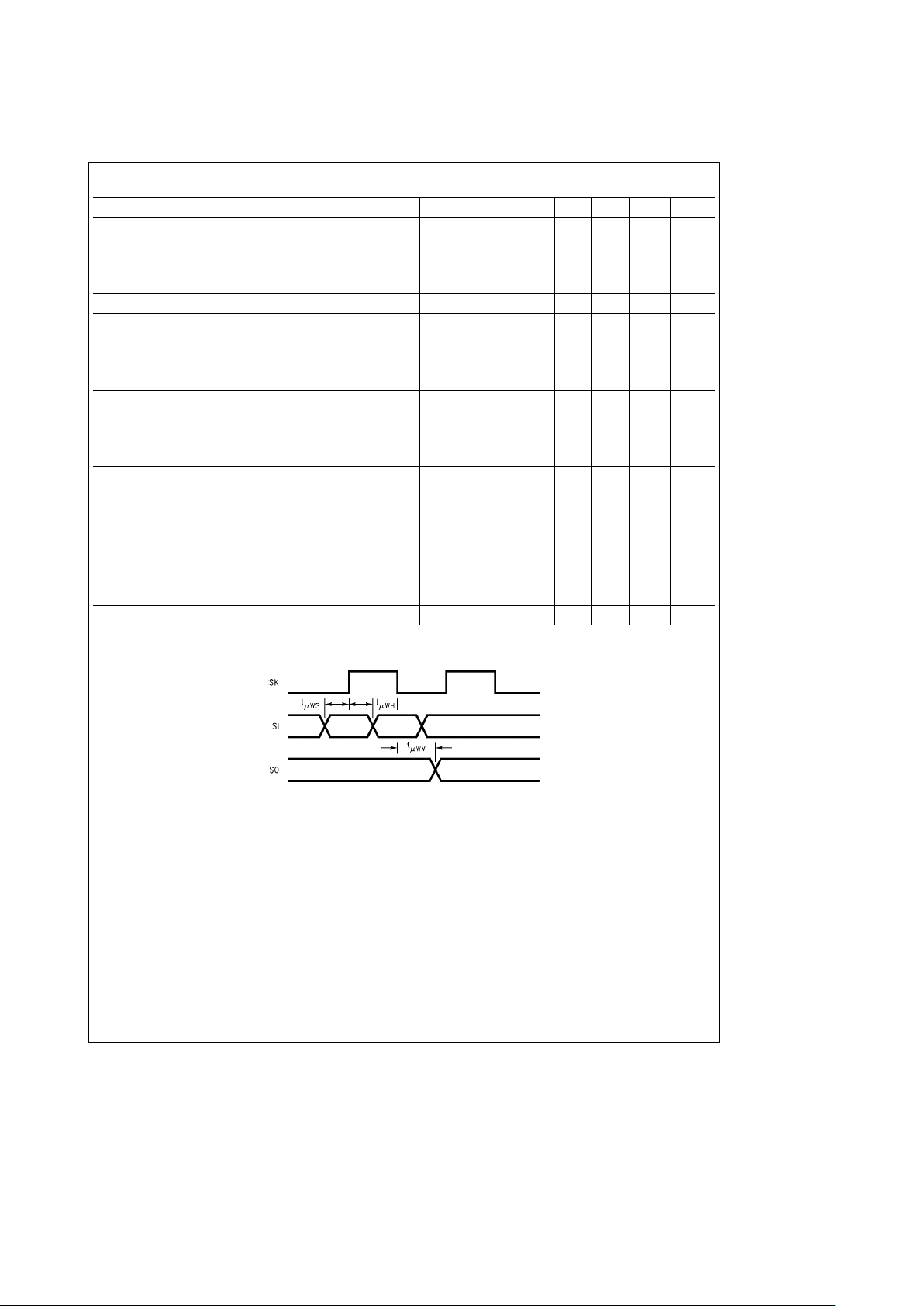
ICSS1001 AC Electrical Characteristics (
b
40§CkT
A
k
a
85§C)
Symbol Parameter Conditions Min Typ Max Units
(tc) Instruction Cycle Time
Crystal/Resonator V
CC
t
4.0V 1.0 DC
ms
2.5
s
V
CC
s
4.0V 2.5 DC
R/C Oscillator V
CC
t
4.0V 3.0 DC
2.5
s
V
CC
s
4.0V 7.5 DC
CKI Clock Duty Cycle (Note 1) feMax 40 60 %
t
SETUP
Inputs
t
HOLD
V
CC
t
4.5V 200
ns
2.5
s
V
CC
s
4.0V 500
V
CC
t
4.5V 60
2.5
s
V
CC
s
4.0V 150 ns
(t
PD1,tPD0
) Output Propagation Delay C
L
e
100 pF, R
L
e
2.2k
SK, SO V
CC
t
4.5V
ms
2.5
s
V
CC
s
4.0V 0.7
All Others V
CC
t
4.5V 1
2.5
s
V
CC
s
4.0V 2.5
(t
UWS
) MICROWlRE
(t
UWH
) Setup Time (Note 1) 20
ns
(t
UPD
) Hold Time (Note 1) 56
Output Propagation Delay 220
Input Pulse Width (Note 2)
Interrupt High Time 1
t
c
Interrupt Low Time 1
Timer 1, 2 High Time 1
Timer 1, 2 Low Time 1
Reset Pulse Width (Note 1) 1.0 ms
Note 1: Parameter characterized but not tested.
Note 2: t
c
e
Instruction Cycle Time.
TL/DD/11727– 5
10
Page 11
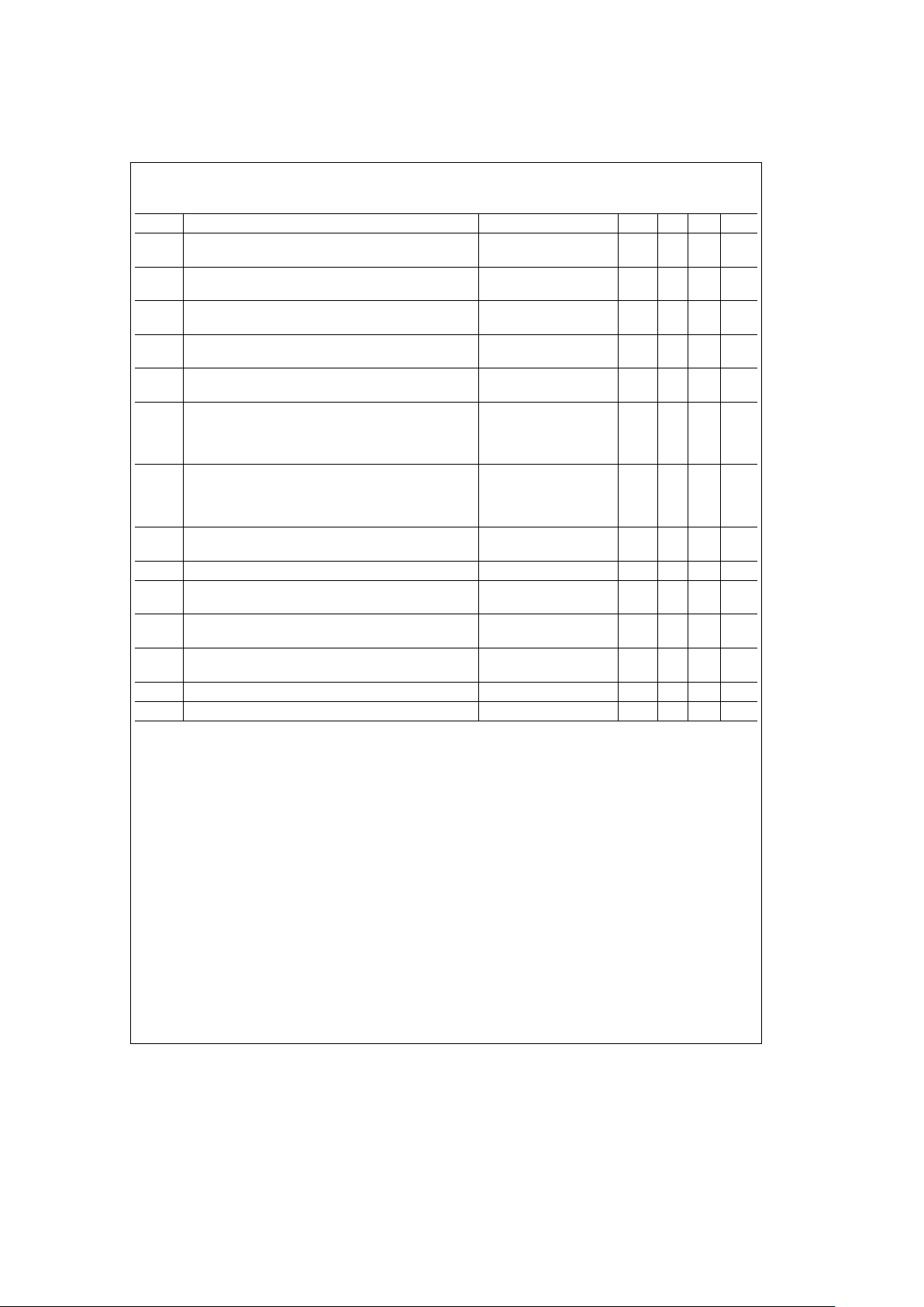
ICSS1002 DC Electrical Characteristics
Specified at V
CC
e
5Vg10%, V
SS
e
GND, over all temperature ranges unless otherwise specified.
Symbol Parameter Conditions Min Typ Max Units
V
IL
Low Level Input Voltage (Note 1) V
CC
e
4.5V
V
TTL Level 0.8
V
IH
High Level Input Voltage (Note 1) V
CC
e
5.5V
V
TTL Level 2.0
V
T
a
Positive-Going Threshold VoltageÐSchmitt Trigger (Note 1) V
CC
e
5.5V
3.9 V
V
T
b
Negative-Going Threshold VoltageÐSchmitt Trigger (Note 1) V
CC
e
5.5V
1.0 V
V
H
Hysteresis VoltageÐSchmitt Trigger (Note 1) V
CC
e
5.5V
1.0 1.6 V
I
IL
Low Level Input Leakage Current V
IN
e
GND, V
CC
e
5.5V
Without Pull-Down Resistor
b
10
mA
With Pull-Up Resistor
b
200
With Pull-Down Resistor
b
10
I
IH
High Level Input Leakage Current V
IN
e
V
CC
e
5.5V
Without Pull-Down Resistor 10
mA
With Pull-Up Resistor 10
With Pull-Down Resistor 200
V
OL
Low Level Output Voltage I
OL
e
4 mA, V
CC
e
4.5V 0.5
V
Reset I
OL
e
12 mA, V
CC
e
4.5V 0.5
V
OH
High Level Output Voltage I
OL
eb
4 mA, V
CC
e
4.5V 3.7 V
I
OZL
Low Level Output Leakage Current (Note 2) V
O
e
GND, V
CC
e
5.5V
b
160 mA
V
IN
e
V
IL
I
OZH
High Level Output Leakage Current (Note 2) V
O
e
V
CC
e
5.5V
160 mA
V
IN
e
V
IL
I
CC
Power Supply Current Drain, DC (Note 3) V
CC
e
5.5V
1mA
CINInput Capacitance (Note 1) 20 pF
C
OUT
Output Capacitance (Note 1) 20 pF
Note 1: Specification is guaranteed by design. This test cannot be performed unless a hook-up to a special output is defined.
Note 2: I
OZ
specifications are for output buffers without pull-up or pull-down resistors.
Note 3: DC means at power on with CLK and POWER ON RC inputs low, all other signal pins open.
11
Page 12
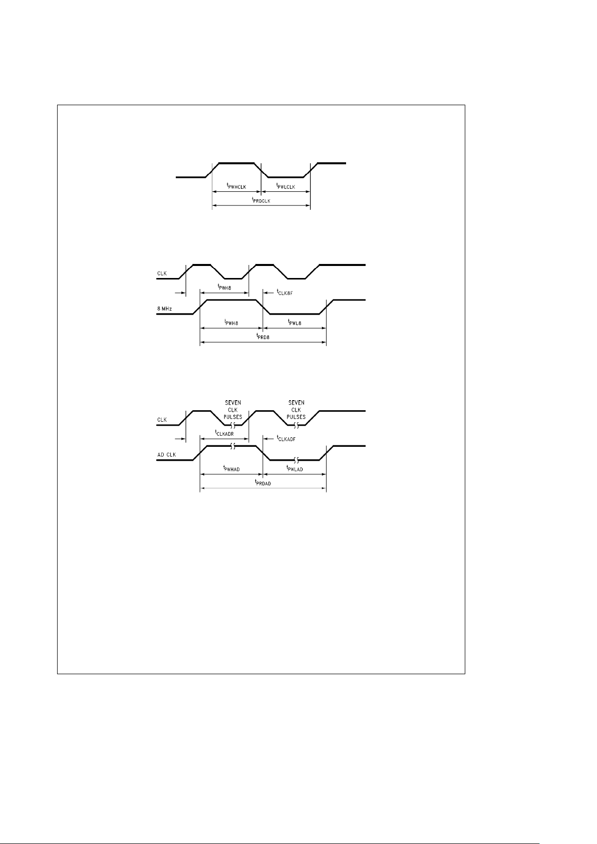
ICSS1002 AC Electrical Characteristics
The AC Electrical Characteristics for the ICSS1002 are not measured. They are guaranteed by design, unless otherwise noted.
The CLK input should be a 16 MHz signal with a period of 62.5 ns and with t
PWLCLK
and t
PWHCLK
of 31.25 ns 6.25 ns. This is
equivalent to requiring a 50% 10% duty cycle on the CLK input. See
Figure 2
.
TL/DD/11727– 6
FIGURE 1. Clock (CLK) Input
8 MHz Output
With a 16 MHz input on CLK, the 8 MHz output will be an 8 MHz square wave with a t
PRD8
of 125 ns and with t
PWH8
and t
PWL8
of 62.5 ns. The 8 MHz signal will transition on rising edges of the CLK signal.
TL/DD/11727– 7
FIGURE 2. 8 MHz Output
AD CLK Output
With a 16 MHz input on CLK, the AD CLK output will be a 1.0 MHz square wave with a t
PRDAD
of 1.0 ms and with t
PWHAD
and
t
PWLAD
of 0.5 ms. The AD CLK signal will transition on rising edges of the CLK signal.
TL/DD/11727– 8
FIGURE 3. AD CLK Output
12
Page 13
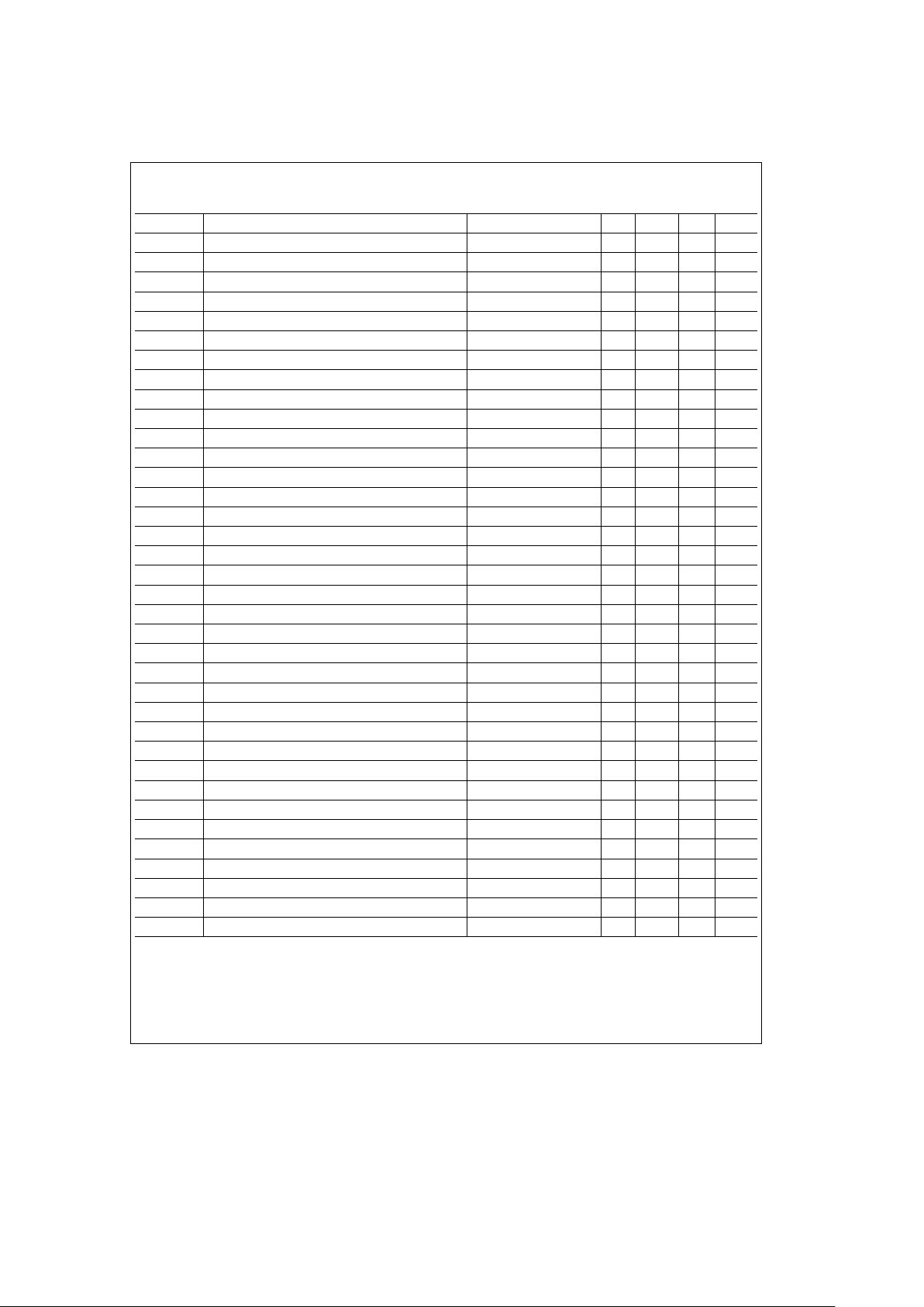
ICSS1002 AC Electrical Characteristics (Continued)
All specifications guaranteed by simulation.
Symbol Parameter Conditions Min Typ Max Units
TPRDCLK CLK Period 62.5 ns
TPWLCLK CLK Pulse Width Low 25 31.25 37.5 ns
TPWHCLK CLK Pulse Width High 25 31.25 37.5 ns
TPRD8 8 MHz Period 125 ns
TPWL8 8 MHz Pulse Width Low 62.5 ns
TPWH8 8 MHz Pulse Width High 62.5 ns
TPWK8R Propagation Delay CLK to 8 MHz Going High 30 ns
TCLLK8L Propagation Delay CLK to 8 MHz Going Low 30 ns
TPRDAD AD CLK Period 1000 ns
TPWLAD AD CLK Pulse Width Low 500 ns
TPWHAD AD CLK Pulse Width High 500 ns
TCLKADR Propagation Delay CLK to AD CLK Going High 40 ns
TCLKADL Propagation Delay CLK to AD CLK Going Low 40 ns
TCKSIH Propagation Delay CSD Bus Valid to SI Valid 30 ns
TSKSI Propagation Delay SK Going Low to SI Next Value 30 ns
TPWHSK Minimum Pulse Width High for SK 50 ns
TPWLSK Minimum Pulse Width Low for SK 50 ns
TCDSIL Propagation Delay CSD Bus Low to SI TRI-STATE 40 ns
TSUCDSK Setup of CSD Bus Valid to SK Going High 20 ns
TSUSOSK Setup of SO Valid Data to SK Going High 20 ns
THSOSK Hold of SO Valid Data after SK Going High 20 ns
THCDSK Hold of CSD Bus Valid after SK Going High 20 ns
TSUSTSK Setup of SK Going High to STROBE Going High 50 ns
TCDRX Propagation Delay CSD Bus Low to RXRDY High 30 ns
TSURXRD Setup of RXRDY Going High to RD Going Low 20 ns
TSUSTRD Setup of STROBE Going High to RD Going Low 20 ns
TRDRX Propagation Delay RD High to RXRDY High 30 ns
TRDDBL Propagation Delay RD Going Low to Data Bus Valid 30 ns
TRDDBH Prop. Delay RD Going High to Data Bus TRI-STATE 30 ns
TPWRD Minimum Pulse Width Low for RD 50 ns
TCDTX Propagation Delay CSD Bus Low to TXRDY High 30 ns
TSUTXWR Setup of TXRDY Going High to WR Going Low 20 ns
TSUDBWR Setup of Data Bus Valid to WR Going Low 20 ns
TWRTX Propagation Delay WR High to TXRDY Low 30 ns
THDBWR Hold of Data Bus Valid after WR Going Low 20 ns
TPWWR Minimum Pulse Width Low for WR 50 ns
13
Page 14
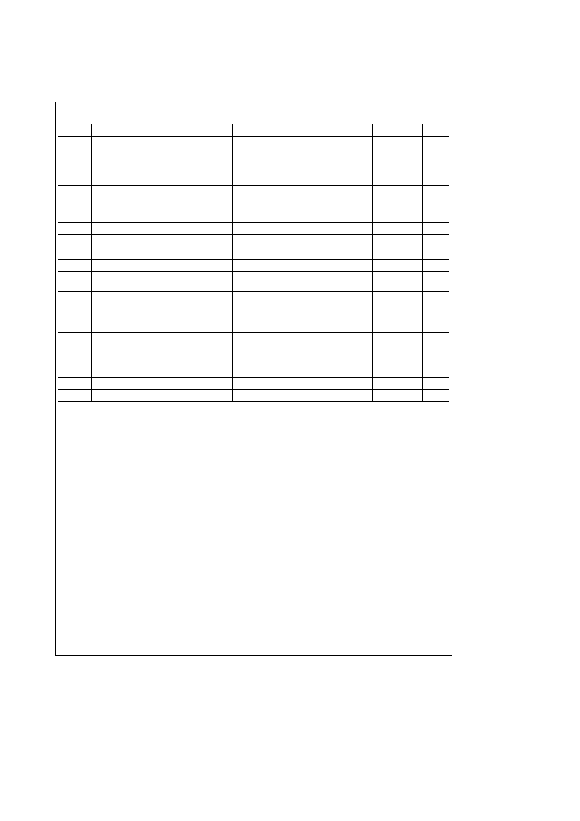
ICSS1003 DC Electrical Characteristics
Symbol Parameter Conditions Min Typ Max Units
I
IH
Input Leakage Current High V
IN
e
V
CC
e
5V, V
EE
eb
5V 10 mA
I
IL
Input Leakage Current Low V
IN
e
0V, V
CC
e
5V, V
EE
eb
5V
b
10 mA
V
IL
Input Low Voltage, TTL Input V
CC
e
5V, V
EE
eb
5V 0.8 V
V
IH
Input High Voltage, TTL Input V
CC
e
5V, V
EE
eb
5V 2.0 V
V
OL
Output Low Voltage I
OL
e
2 mA, V
CC
e
5V 0.5 V
V
OH
Output High Voltage I
OH
eb
400 mA, V
CC
e
5V 2.4 V
V
OSF
Filter Operational Amplifier Offset Voltage V
CC
e
5V, V
EE
eb
5V
b
10 10 mV
V
OSG
Gain Control Amplifier Offset Voltage V
CC
e
5V, V
EE
eb
5V
b
20 20 mV
I
IB
Gain Control Filter Input Bias Current V
CC
e
5V, V
EE
eb
5V
b
55mA
V
SWP
Minimum Output Voltage Swing Positive V
CC
e
5V, V
EE
eb
5V 2.5 V
V
SWN
Minimum Output Voltage Swing Negative V
CC
e
5V, V
EE
eb
5V
b
2.5 V
V
SWPD
Minimum Output Voltage Swing Positive: V
CC
e
5V, V
EE
eb
5V
4.0 V
Driver D1 and D2 Outputs
V
SWND
Minimum Output Voltage Swing Negative: V
CC
e
5V, V
EE
eb
5V
b
4V
Driver D1 and D2 Outputs
I
OUTP
Minimum Output Current Drive Positive: V
CC
e
5V, V
EE
eb
5V
30 mA
Driver D1 and D2 Outputs
I
OUTN
Minimum Output Current Drive Negative: V
CC
e
5V, V
EE
eb
5V
b
30 mA
Driver D1 and D2 Outputs
I
CC
Positive Power Supply Current (Note 1) V
CC
e
5V 100 mA
I
EE
Negative Power Supply Current (Note 2) V
CC
e
5V
b
100 mA
C
IN
Input Capacitance (Note 3) 20 pf
C
OUT
Output Capacitance (Note 3) 20 pf
Note 1: ICCconditions.
Note 2: I
EE
conditions.
Note 3: Specification is guaranteed by design.
14
Page 15
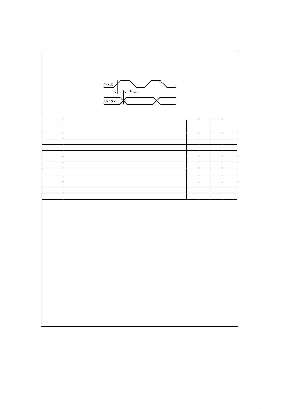
ICSS1003 AC Electrical Characteristics (Continued)
The AC Electrical Characteristics for the ICSS1003 are not measured. They are guaranteed by design, unless otherwise noted.
AD CLK to AD Bus
The AD bus (AD3 – AD0) changes on the rising edge of the AD CLK.
TL/DD/11727– 9
FIGURE 4. AD CLK to AD Bus
Symbol Parameter Min Typ Max Units
FMAXAD Maximum Clock Frequency AD CLK 1.0 MHz
TCLKAD Propagation Delay AD CLK to AD Bus (Note 1) 50 ns
BWF Filter Operational Amplifier Small Signalb3 dB Bandwidth 5 MHz
SRF Filter Operational Amplifier Output Slew Rate 2.5 V/ms
BWGMIN Gain Control Amplifier Small Signalb3 dB Bandwidth at Maximum Gain Setting 2.5 MHz
BWGMAX Gain Control Amplifier Small Signalb3 dB Bandwidth at Maximum Gain Setting 0.3 MHz
SRG Gain Control Amplifier Output Slew Rate (V
OUT
e
5VPP) 2.5 V/ms
GCS Gain Control Amplifier Gain Selection Delay 1.0 ms
ROD Gain Control Amplifier Overdrive Recovery Time 3 ms
BWD Driver Amplifier Small Signalb3 dB Bandwidth 0.5 MHz
SRD Driver Amplifier Output Slew Rate (V
OUT
e
5VPP) 2.5 V/ms
ENDRV Enable/Disable Delay of Driver from DRV EN 100 ms
Note 1: Estimated, but not tested or guaranteed.
15
Page 16
Network Operation
SYNCHRONIZATION AND NETWORK ACQUISITION BY
SLAVES
This section describes the process through which a network
is initialized, and through which additional subscribers
(Slaves) join the network.
Slave Initialization
Upon initialization, a Slave must search for and find the tune
and bit rate currently in use. It proceeds as follows:
1. All tunes are searched, starting with the highest.
2. Within each tune search, bit rate is searched, starting at
the highest bit rate.
3. Within each bit rate, gain is optimized using the peak
search procedure described in 1 and 2.
4. If a valid packet is obtained during this process, then the
Slave knows the tune and switches to it, entering run
mode. The Slave knows a packet is valid when the error
code checks correctly.
5. If not, the Slave proceeds to search all the possible
tunes and bit rates, remaining on each combination for
four packet times.
This process is repeated until a valid packet is heard.
Master Initialization
The Master starts by performing the Slave initialization sequence to see if a network with the same network address
already exists. If so, it will listen and wait for that Master to
falter. When it no longer detects the other Master, it will step
in and try to take over.
Application software developed for IC/SS must keep track
of the number of Masters and their addresses, as the dueling Master situation is impossible to prevent and can be
very confusing.
If the Master cannot find a Slave with its own network address, it will proceed to the next frequency channel, and
repeat the process.
Network Runtime Operation
In order to keep the system gain and tune selection optimal,
the network is always kept active. In network mode, the
Master runs autopoll whenever there is no required host
traffic.
Once a network is established with one or more Slaves, the
tune control will be performed as described above.
ERROR CODING AND TIME DIVERSITY
In addition to frequency-dependent noise which is combated by the adaptive frequency hopping described above,
power lines suffer from impulsive noise. Impulsive noise
bursts occupy all frequency bands for relatively short periods, often less than one bit time. This noise tends to be
synchronous at 100 Hz or 120 Hz due to its origin.
In network mode and in the software loopback function of
transparent mode, two techniques are employed to reduce
sensitivity to impulse noise: error correction and overlay of
retries.
Error Detection
Bytes transmitted over the network are 9 bits long, 8 bits of
data plus a parity bit. This allows the receiving unit to detect
single-bit errors in any byte.
In addition a 27 bit error code is appended to the end of
each packet. It consists of three bytes plus byte parity. The
three bytes together comprise a CRC-24. This error coding
allows implementation in software in real time, meets IEC
and CENELEC requirements, and works well with the overlay technique.
Overlay of Retries
Overlay of retries means saving those portions of earlier
blocks which were not corrupted, so that on a subsequent
retry a complete message can be assembled. A single impulse noise burst should only affect one or two bytes, and,
since the timing of retries is arbitrary due to variable block
length, it is unlikely that impulsive noise bursts will hit the
same portion of a message on successive retry attempts.
If a given byte of a packet has invalid parity, the receiver will
continue to collect data for the remainder of the packet, and
will store those bytes with valid parity in the receive buffer.
However, if the first byte, which contains the packet length,
is corrupted, the entire packet must be abandoned.
On subsequent retries, if any byte is invalid, it will not be
written to the receive buffer, but the corresponding byte already stored from the previous transmission or transmissions will be used. At the end of the packet, if the 27 bit
error code is found to be valid, then a complete packet has
been assembled and it will be output as such.
This approach allows the system to communicate successfully even in an environment so noisy that every packet has
uncorrectable errors. It is only necessary that each byte get
through once.
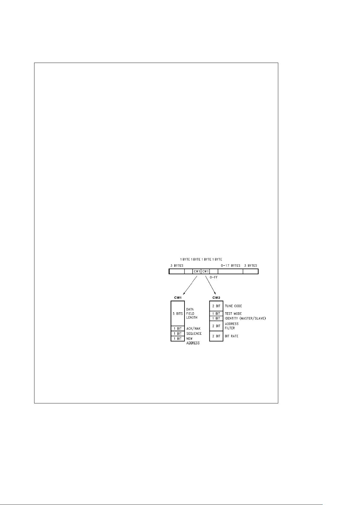
PACKET STRUCTURE
Data is sent between units in packets of variable length,
containing from zero to 17 bytes of data, plus protocol information and error coding. The packet format is shown in
Fig-
ure 5
.
TL/DD/11727– 10
FIGURE 5. Packet Structure
For all communication modes between Master and Slaves
except broadcast, a block-ahead acknowledgment procedure is used. This ensures that packets are retried if errors
cannot be corrected. The number of retries is limited by a
retry count parameter. The application program is thus guaranteed that either a packet will be delivered to the far end,
or the application program will be notified that this is impossible.
16
Page 17

Network Operation (Continued)
Two different maximum retry count levels are stored in firmware. The higher value is used once a link has been established.
In the case of broadcast mode, each packet is simply sent
eight times, and correct receipt by all the Slaves is not guaranteed.
LINK AND NETWORK LAYERS
This section presents a description of link and network layer
operation.
Address Structure
The Master carries a two-bit network address, set via the
initialization command, or by default at 00.
The Slave carries a two-bit network address, and an eightbit Slave address. The network address is set via the initialization command, or by default at zero. The Slave address is
set by the initialization command, by hardware dip switches
if connected, or by default to FF (Hex). Slave addresses 00
and FF are reserved; 00 is an illegal attribute for a Slave,
and is used internally for broadcast; FF is reserved for a
contention channel and for address assignment.
The Slave will only respond to a packet from a Master that
bears both network and Slave addresses which match its
own.
This structure permits the creation of a network containing
254 Slaves and one Master, up to four such networks can
operate concurrently on different frequency-division-multiplexed channels. In this configuration, the benefits of frequency-hopping are not available, but higher aggregate
throughput is obtained if the channel quality is relatively
good. The Master’s host can create one network with 1016
slaves by changing the Master’s address field periodically.
General Command Structure
The system can operate either in transparent mode, where
the physical layer is available to the host, or in network
mode, where the link layer is available to the host. This
choice is determined by the polarity of the NE/TRNSP pin,
which is read by the microprocessor during its initialization
sequence.
In transparent mode, the data present at the input is transferred to the output of all other modems on the same electrically connected power line bus. Addressing, media access
control, error control and error recovery are the responsibility of the user. In this mode, the controller is not in the data
path, and is used only to establish bit rate, frequency, and
gain.
In network mode, a set of commands is provided which implement a Master-Slave local area network protocol, optimized for hierarchical control and data acquisition applications. The network mode includes a host-modem command
set which includes:
#
Network Commands, which permit:
Ð polling of a range of Slave addresses in order to collect
data
Ð broadcast of data to all Slaves
Ð a continuous, full duplex error-free link to any individual
address
#
Test Commands, which permit:
Ð installation
Ð debugging
Ð network qualification
#
Commands which control physical layer operation.
The detailed syntax of all the commands is described below.
If a modem receives an illegal command code (character
following
kk
ESCllis not one of the command codes
listed for Master or Slave, as the case may be), it will output
kk
ESC
ll kk
BELLll. If the modem is a Master, it will
return to default state (autopoll address 1).
Commands are distinguished from data in different ways,
depending on whether the chip set is configured for serial or
parallel operation.
In serial operation, commands and status responses are
prefixed by an
kk
ESCllcharacter. The interface reverts
to data mode after transfer of a legal command syntax (or a
sequence comprising illegal syntax). To transmit an escape
character in the application data stream, send
kk
ESC
llkk
ESCll.
In parallel mode, commands and responses are distinguished from data by two pins on the parallel interface:
COMMAND for input to the chip and STATUS for output
from the chip. The respective pin should be placed in HIGH
state by the device performing data output prior to the availability of data. A signal on one of these two pins replaces
the
kk
ESCllcharacters described for the serial port;
kk
ESCllcharacters are not required to designate com-
mands when operating in parallel mode.
The symbol[CMD]will be used here to indicate the command signal. In serial mode[CMD]stands for an
kk
ESCllcharacter. In parallel mode[CMD]means that
either the COMMAND or STATUS line was asserted (set
LOW). In either case,[CMD]designates the following characters to be a command or a response, not data. The length
of each command or response is determined by context.
Every command will generate a response proceeded with a
[
CMD]and followed by an
kk
ACKll,kkNAKll,
kkSIllorkkSOll
. After issuing a command to its
modem, a host should not send anything (neither data nor
new command) to the modem until it receives a response to
the last command from the modem. Anything sent to the
modem after issuing a command but before receiving a response to it will be discarded.
A Flush Buffer Command is provided to handle the following
situation: If a Slave’s host fails during reception of data from
the Slave and leaves the Slave’s output inhibited by the flow
control lines, the result will be that the Slave’s buffer fills
with data. The Slave will then stop accepting data, causing
the Master’s buffers to fill up. The Master in turn signals its
host, via flow control, to stop sending data. In this situation
the Master’s host will not be able to transfer further data to
any Slave until the data buffered by the Master is successfully transmitted. In this case, the Master’s host can issue
the Flush Buffer Command, which will destroy data currently
buffered and waiting to be sent, and return the system to
default autopoll mode.
The timing of the interaction between Master’s host, Master,
Slave, and Slave’s host can best be understood by reviewing the examples that follow, which are based on serial
mode operation.
17
Page 18

Command Descriptions
Command: Autopoll
Syntax:
[
CMD
]
k
Ctrl-ClkArg 1lkArg 2
l
Arg 1: Lower limit of the Slave address space (bina-
ry)
Arg 2: Upper limit of the Slave address space (bina-
ry)
Response: (If link was acquired)
[
CMD
]
kSOlk
Addr of SlavelkData
l
Response: (If link was not acquired)
[
CMD
]
kSIlk
Addr of Slave
l
Response: (If link was broken)
[
CMD
]
kSIlk
Addr of Slave
l
Functionality
Using the address specified, the Master attempts to establish a continuous link to the Slave. If a link is established,
[
CMD
]
kSOl
are transmitted to the host followed by any
data received from the Slave. When the Master receives a
packet from the Slave with no data, the Master will assume
that the Slave has transmitted all of its data which will
prompt the Master to break the link and send[CMD
]
kSIl
to its host and increment the Slave address and repeat the
described sequence for the next Slave. When the Slave address range is exhausted, the Master will wrap around the
Slave address space and proceed with a new cycle of autopoll.
Command: Broadcast
Syntax:
[
CMD
]
k
Ctrl-A
l
Response:[CMD
]
k
ACKlk0
l
Functionality
Enter broadcast mode of operation at the Master. The Master will remain in broadcast mode until a new command is
issued by the host.
Command: Continuous Link
Arg 1:
[
CMD
]
k
Ctrl-DlkArg 1
l
Response: (If link was acquired)
[
CMD
]
k
ACKlkAddr of SlavelkData
l
Response: (If link was not acquired)
[
CMD
]
k
NAKlkAddr of Slave
l
Response: (If link was broken)
[
CMD
]
k
NAKlkAddr of Slave
l
Functionality
Establishes continuous point-to-point link to a Slave.
Command: Network Test Mode (Binary)
Syntax:
[
CMD
]
k
Ctrl-BlkArg 1lkArg 2
l
Arg 1: Lower limit of the Slave address space (Input
as a binary number)
Arg 2: Upper limit of the Slave address space (Input
as a binary number)
Response:[CMD
]
k
ACK
l
Command: Get Test Results
Syntax:
[
CMD
]
k
Ctrl-F
l
Response:[CMD
]
k
DLElkByte 1lkByte 2l...
k
Byte 9lkByte 10lkByte 11
l
Byte 1eNumber of test cycles completed.
Byte 2eNumber of Slaves that responded.
Byte 3eMSByte of the number of detected bytes re-
ceived in error.
Byte 4
e
LSByte of the number of detected bytes received in error.
Byte 5
e
Number of passed bytes in error.
Byte 6
e
Lowest address of a slave that responded.
Byte 7eHighest address of a slave that responded.
Byte 8eNumber of retries.
Byte 9eNumber of sync timeouts.
Byte 10eNumber of times the first byte of the packet
was received incorrectly.
Byte 11
e
Current tune code.
Functionality
Initiate test mode and output results via the serial link. Results are sent when the maximum amount of information
has been gathered, i.e., before any field of the result buffer
overflows. After the first set of results is sent, the modem
continues test mode normally without spontaneous output.
The very first response from the modem after
k
Ctrl-Blis
the command acknowledgment indicating to the host that
the command has been processed and that the modem is
ready to accept new commands. Following the response
are the test results in the format specified below.
The command acknowledgment format is as follows:
[
CMD
]
k
ACK
l
Output format:[CMD
]
k
DLElkByte 1lkByte 2l...
Data is in binary format.
Command: Test Mode (ASCII)
Syntax:
[
CMD
]
k
Ctrl-KlkArg 1lkArg 2
l
Arg 1: Lower limit of the Slave address space.
Arg 2: Upper limit of the Slave address space.
Response:[CMD
]
k
DLE
lkCRlkLFlk
Space
l
k
ASCII byte of datalkSpacelkASCII byte
of data
l
...
Data is in ASCII Hex format. This output format is supported only in serial mode. In parallel I/O mode, Ctrl-K output is
identical to Ctrl-B output.
Functionality
Same as that for Network Test Mode (Ctrl-B).
Command: Flush Command Buffer and get Software Re-
vision Number
Syntax:
[
CMD
]
k
Ctrl-N
l
Response:[CMD
]
k
ACKlkMajor RevlkMinor Rev
l
18
Page 19
Command Descriptions (Continued)
Functionality
Flush Command Buffer and return Master to default autopoll
state, also return to host current software revision (binary
format).
Command: Set Preamble Length
Syntax:
[
CMD
]
k
Ctrl-MlkLength
l
Response:[CMD
]
k
ACK
l
Functionality
Sets number of bytes of preamble the modem will use.
Command: Chip Reset
Syntax:
[
CMD
]
k
Ctrl-GlkArg 1lkArg 2
l
Arg 1: Lower nibbleeMaster filter
Upper nibblee0 for Slave, 1 for Master
Arg 2: Unit address (1 – 255, 0
e
previous address)
Response:[CMD
]
k
ACK
l
Functionality
Performs a soft reset of the modem allowing change of
identity and addresses.
Command: Chip Status Request
Syntax:
[
CMD
]
k
Ctrl-H
l
Response:[CMD
]
k
ACKlkRetry countlkInformation
byte dependent on unit i.d.
l
Functionality
Returns status information: Retry count and, for Slave, Master filter (upper nibble); or, for Master, currently addressed
Slave address.
Command: Set Tune
Syntax:
[
CMD
]
k
Ctrl-ElkArg 1
l
Arg 1: Tune code (binary number). Ctrl-Aetune 0,
. . . , Ctrl-E
e
tune 4. If an illegal tune code is
passed as an argument, then the frequency
hop mechanism will be reenabled and the current tune will remain unchanged.
Response:[CMD
]
k
ACKlkCurrent tune code (lower
nibble)
l
Functionality
Master: Disables frequency hop mechanism and sets current tune to the value of the argument.
Slave: Sets the current tune to the value of the argument.
LEDs also display the current tune code.
Command: Set Bit Rate
Syntax:
[
CMD
]
k
Ctrl-LlkArg-1
l
Arg 1: Data rate code (binary number) Ctrl-A
e
3200 bps, Ctrl-Be1212 bps, Ctrl-C
e
800 bps, Ctrl-De400 bps. An illegal argument will re-enable automatic data rate control.
Arg 2:
[
CMD
]
k
ACKlkNew Bit Rate
l
Functionality
Sets the modem bit rate based on the value ofkNew Bit
Rate
l
data.kNew Bit Ratelis a two bit value in the upper
two bits of the lower nibble of the byte returned.
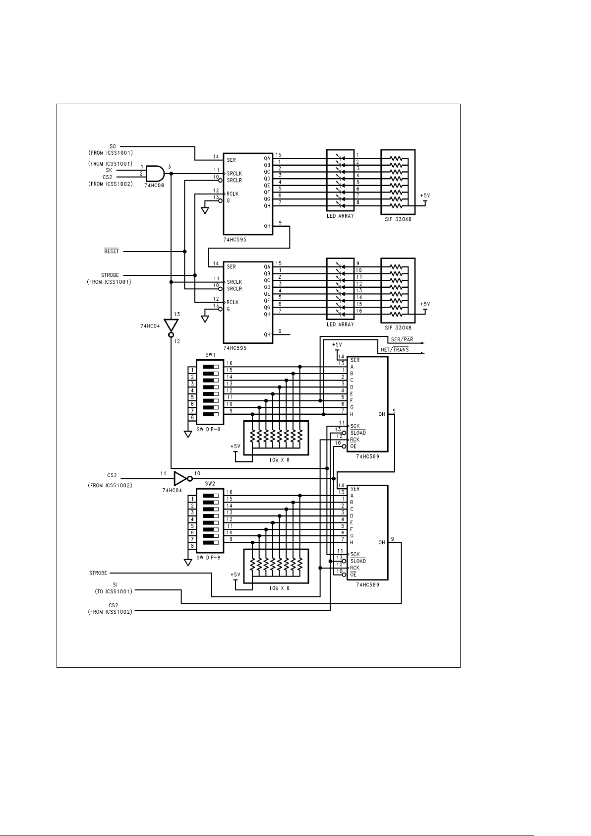
EXTERNAL PARAMETER SETTINGS
Provision is made for setting the baud rate and word structure of the serial interface through external latches, which
may be connected to DIP switches. These are read through
the MICROWIRE interface to the microcontroller during initialization. Refer to
Figure 6
for the interface circuitry required. If the user’s circuit does not include DIP switches
then the default conditions are those corresponding to all
switches off. The parity settings depend on the settings of
the DIP switches as shown in Table IV.
TABLE IV. Parity Control
DIP Switch 1.3 DIP Switch 1.2 Parity
off on odd
on off odd
on on even
off off none
The baud rate depends on the settings of the DIP switches
as shown in Table V.
TABLE V. Baud Rate Settings
DIP DIP DIP Baud
Switch 1.6 Switch 1.1 Switch 1.0 Rate
on off off 300
off on 1200
DIP switch 1.4 is used to configure the host port as serial or
parallel. DIP switch 1.5 is used to configure the modem as
either a Master or a Slave. Refer to Table VI.
TABLE VI. Modem Configuration
DIP Switch DIP Switch
1.4 1.5
on Parallel Slave
off Serial Master
19
Page 20
Command Descriptions (Continued)
TL/DD/11727– 11
FIGURE 6. Suggested Configuration of MICROWIRE Interface for DIPs and LEDs
20
Page 21
Network Command Examples
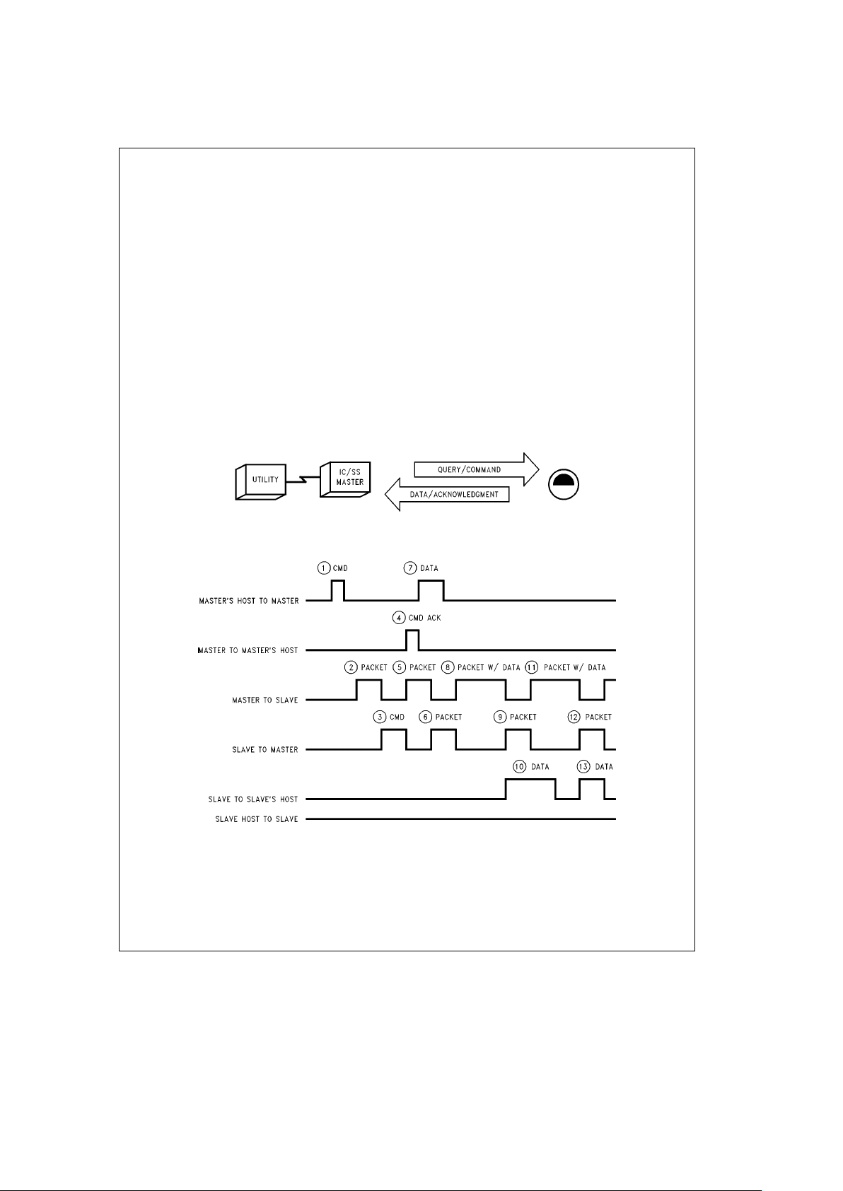
CONTINUOUS LINKS
Figure 6
shows the sequence for continuous link, which is
also diagrammed in
Figure 7
.
1. Host sends Master command to open link to Slave 01.
2. Master sends packet over power line addressed to Slave
01.
3. Slave 01 responds with acknowledgment packet to Master.
4. Master outputs Acknowledgment.
5.[CMD
]
kk
ACK
llkk
addressllto host.
6. Master simultaneously sends packet to Slave.
7. Slave responds with packet to Master.
8. Master host, having received acknowledgment step 4,
sends data to Master, destined for Slave host, which is
buffered in Master.
9. As soon as it receives packet from Slave, Master sends
an additional packet to the Slave, containing data from
host buffered in step 7.
10. Master and Slave continue to trade packets, each
transmitting as soon as it receives a packet from the
other. The packet will contain whatever data has been
buffered, unless the control bits indicate that the prior
packet must be repeated.
11. Slave receives packet (8), and transmits the data it contained to Slave host.
12. Master, having received a packet (9) from Slave, sends
Slave a packet with the rest of the data from Master’s
host, which had not yet arrived in its buffer when packet
(8) was sent.
13. This data is received by the Slave.
14. And sent to Slave’s host.
Packets will continue to be interchanged between the Master and Slave until the link is broken by an appropriate command from the Master’s host. This supports bidirectional
virtual full duplex communication between the two hosts.
TL/DD/11727– 12
FIGURE 7. Continuous Link Mode Diagram
TL/DD/11727– 13
FIGURE 8. Command Interaction: Continuous Link
21
Page 22
Network Command Examples (Continued)
AUTOPOLL
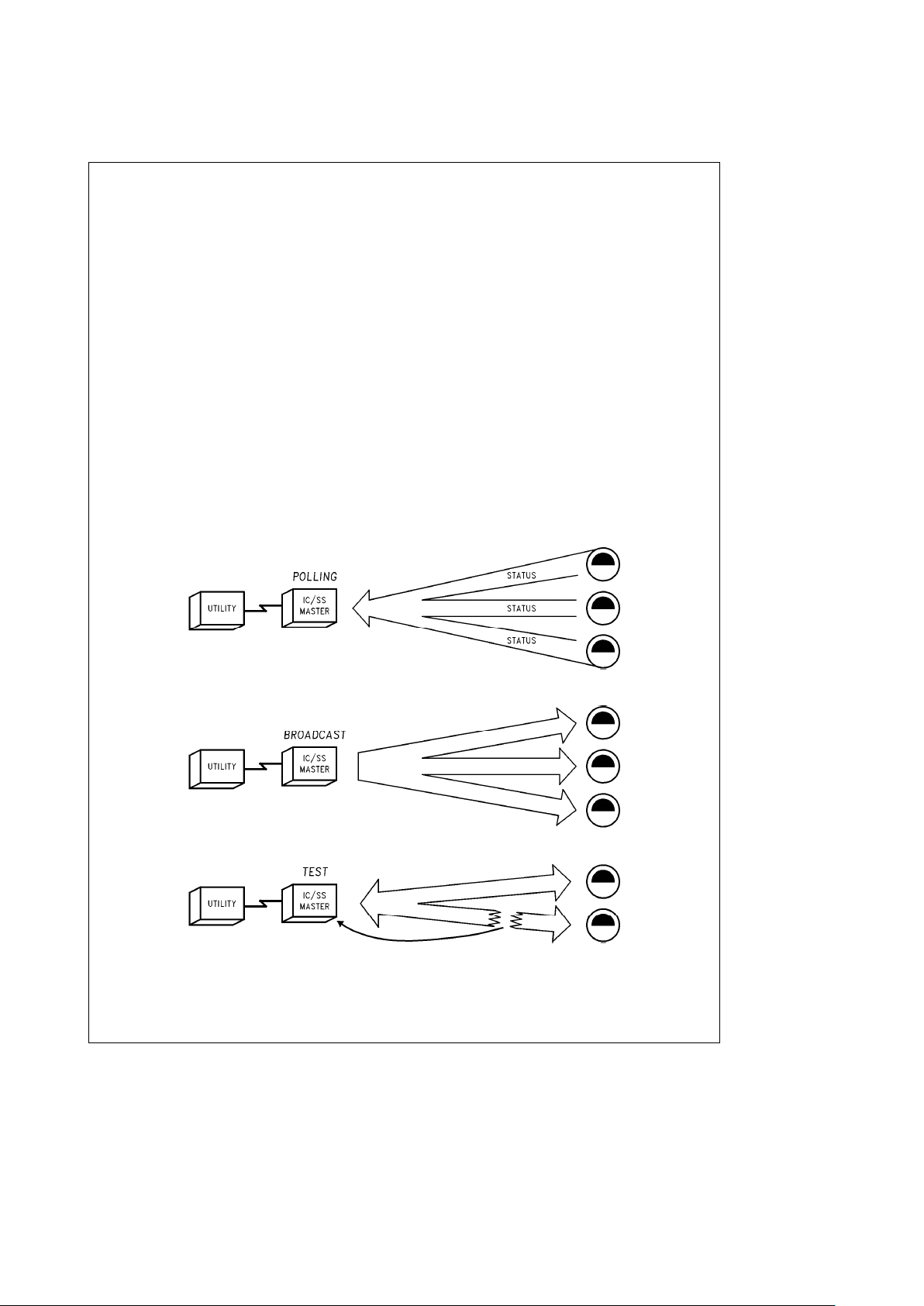
Figure 8
shows the corresponding sequence for the autopoll
command.
1. Slave’s host sends data to Slave, which is buffered by
Slave. Slave will buffer up to 17 bytes, and uses flow
control to prevent overflow.
2. Sometime later, Master’s host issues an autopoll command to Master.
3. Master sends a packet to Slave, containing no data.
4. Slave immediately sends a packet to the Master, containing whatever data has been buffered in step 1.
5. Master receives this packet, and responds with another
packet to the Slave.
6. Simultaneously, Master outputs
[
CMD
]
kkSIllkk
addressll, to Master’s host.
7. While this is going on, Slave’s host might have sent
Slave more data. If so, steps 4 and 5 are repeated. If
there is no more data buffered by the Slave at the time
the packet sent in step 5, arrives, the Slave responds to
the Master with a packet containing no data.
8. The Master receives empty packet causing Master to
break the link and proceed to the next Slave address in
its autopoll cycle. It announces this to the Master’s host
by sending it[CMD
]
kkSOllkk
addressll.
The link will also be dropped after 10 packets have been
transmitted (Rev A setting).
BROADCAST
Broadcast is used when only one way transmission of data
from the Master to all of its Slaves is desired (see
Figure 9
).
All data sent to the Master modem from the Host is transmitted 8 times onto the line. Slave Address 0 is used for
this.
This is useful when it is desirable to have a low cost, one
way communication channel available.
TEST MODE
Test Mode (see
Figure 10
) is a built-in application in the
IC/SS chip set that is most useful for evaluating the potential performance of an end user application using IC/SS
over a variety of power line conditions. All of the other
IC/SS functions provide network layer services for Host
Computers to which they are connected. They assume the
existence of one or more applications (in the attached Host
Computers) that utilize these services.
TL/DD/11727– 14
FIGURE 9. Autopoll Mode Diagram
TL/DD/11727– 15
FIGURE 10. Broadcast Mode Diagram
TL/DD/11727– 16
FIGURE 11. Test Mode Diagram
22
Page 23
Network Command Examples (Continued)
TL/DD/11727– 17
FIGURE 12. Test Report Structure
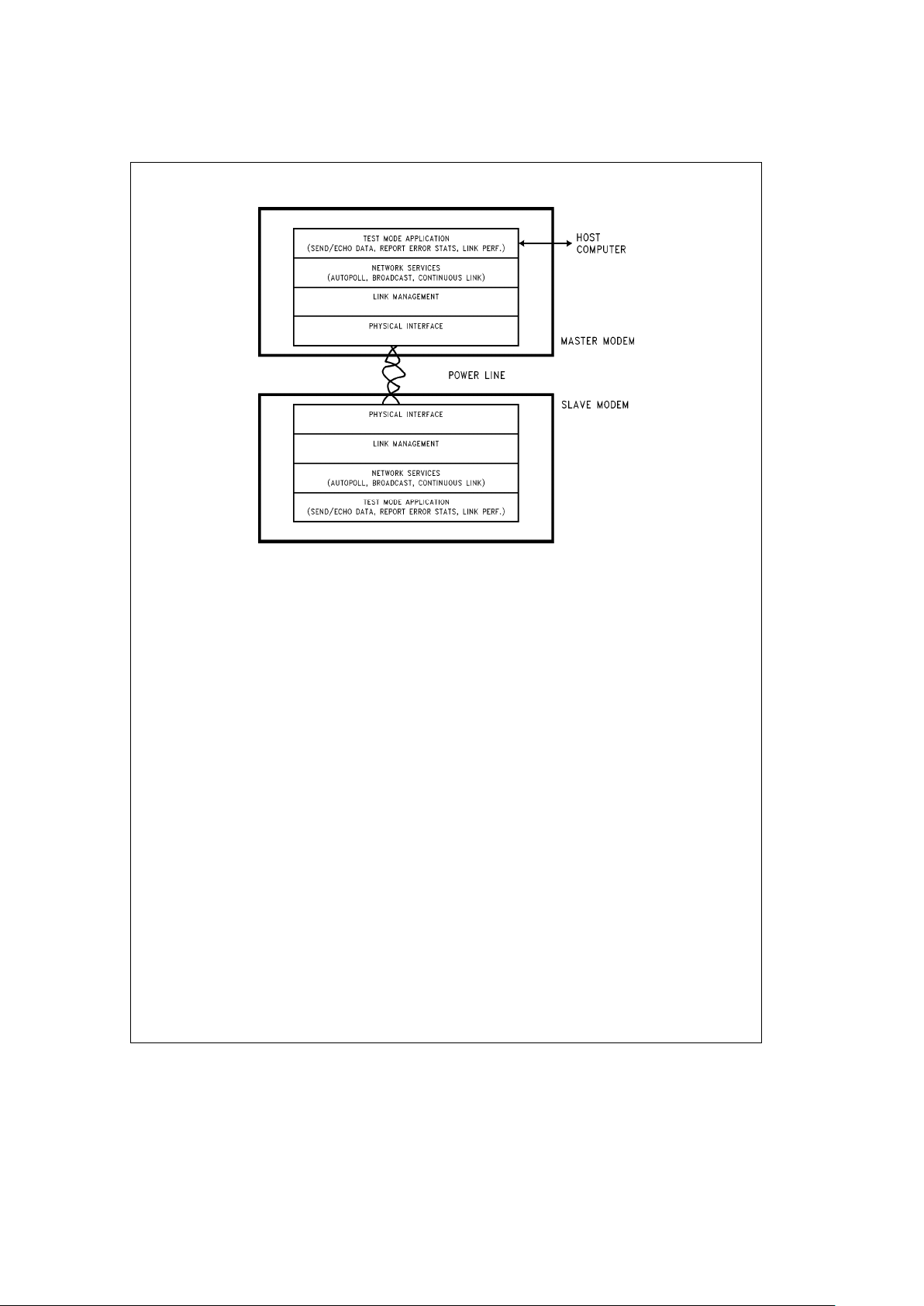
Test Mode includes a simple set of applications that use the
services provided by the other IC/SS functions. The embedded Test Mode application in the Master modem exchanges
data with the test mode applications embedded in one or
more Slave modems, and generates a report in either ASClI
or Binary form.
This data exchange is used to measure the performance of
the modems and the conditions on the power line. The embedded Test Mode application keeps statistics on the exchange of data with other modems, tracking data integrity
and communications performance (retries, parity errors,
which Slaves responded, tune code used, etc.). This information is formatted into a report which is transmitted to the
Master’s Host computer. This is illustrated in
Figure 11
.
If you have known power line conditions, the test mode information lets you evaluate the IC/SS modem’s performance. In a field installation, test mode can be used periodically by the host computer to evaluate the power line conditions, and perhaps determine whether to perform or defer a
given application operation.
ASClI versus Binary Test Mode
The major differences are that Binary Test Mode does not
automatically generate a reportÐyou must use the Control
F command (Get Test Results) to get a reportÐand the
report is sent out as 11 bytes of binary information, rather
than being formatted as ASCII hex with space delimiters
and a CR/LF at the end of the report.
Operation of Test Mode
Test Mode works through the normal IC/SS network layer.
This means that all the mechanisms in IC/SS that are used
to get information correctly over the power line are in use
during Test Mode. Gain, Bit Rate and Tune Code will be
adjusted according to the measured Bite error Rate, just as
in all other commands. The Packet Overlay mechanism will
be used to try to make good packets out of damaged ones.
The Test Mode Report
The Test Mode application generates a Test Mode Report
which is either automatically transmitted (via ASCII Test
Mode command) or transmitted on demand (via the Binary
Test Mode and the Get Test Results commands) to the attached Host.
When in ASCII Test Mode, the time between reports can
range from 20 seconds to 4.5 minutes. This time is dependent upon two thingsÐthe modem to modem bit rate and
the behavior of the Slaves being tested. The Test Mode
application will generate its report when count of any one of
information categories being tracked threatens to overflow.
Any category getting within 32 (20 hex) of overflow will
cause the test mode report to be generated.
Example: Test mode command
e
k1Blk0Blk01l
k
01l(ASCII hex data)
Slave 1 is connected and working. Test Mode will
likely do E0 hex (224 decimal) test cycles (byte 1)
and then generate a test report.
Example: Test mode command
e
k1Blk0Blk01l
k
02l(ASCII hex data)
Slave 1 is connected and working, Slave 2 is disconnected.
Test Mode will likely do E0 hex (224 decimal) retries (byte 8)
and 36 hex (54 decimal) test cycles and then generate a
test report.
23
Page 24
Chip Set Operation
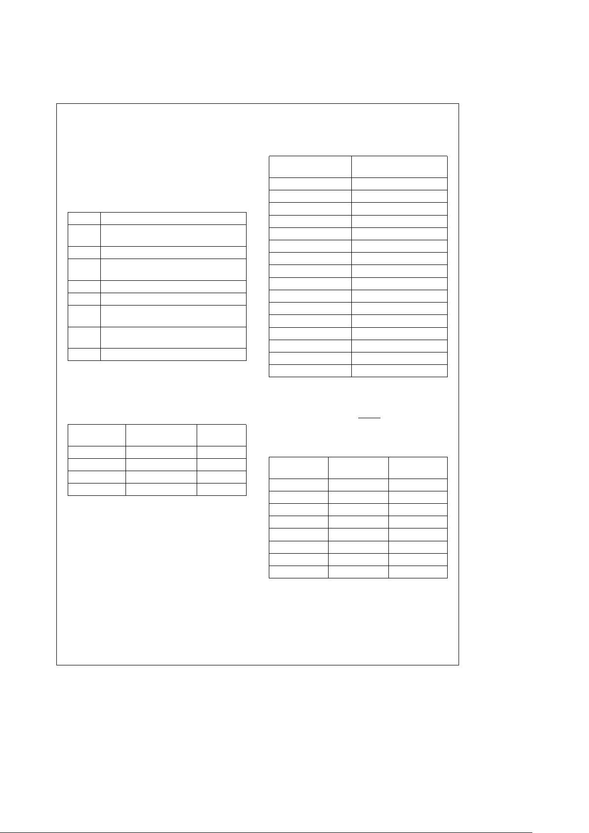
The CSD (Control Serial Data) bus (CSD2, CSD1, and CSD)
is used to select which function the controller interface will
perform. The following table details the CSD bus decode.
When switching functions, e.g., changing the CSD bus, the
CSD bus must first be set to zero (000) before changing to a
new value. If this is not done, it is possible to generate a
false RxRDY signal.
Note: NEVER USE state (111) as this will generate a false RxRDY signal
during transition to another setting.
TABLE VII. CSD Bus Settings
CSD Function
000 (0) Not used. Preferred address when the
interface is not in use.
001 (1) Set Analog Chip gain control amplifier gain.
010 (2) Generate CS2 signal to enable external
MICROWIRE ports.
011 (3) Set BRM.
100 (4) Set bit rate.
101 (5) MICROWIRE interface write to parallel data
bus.
110 (6) Parallel data bus write to MICROWlRE
interface.
111 (7) Do not use, see Note above.
When the CSD bus is set to four (100), the MlCROWIRE
interface will write the Data Rate Control Register. Only the
two LSBs of the MlCROWIRE 8-bit word will be used. The
six MSBs will be discarded. The following table details the
data rate settings.
TABLE VIII. Data Rate Control Register Settings
MICROWIRE Data Rate Data Rate
Data D7–D0 Control Register (bits/sec)
xxxxxx00 00(0) 3200
xxxxxx01 01(1) 1212
xxxxxx10 10(2) 800
xxxxxx11 11(3) 400
When the CSD bus is set to three (011), the MICROWIRE
interface will write the BRM (Binary Rate Multiplier) control
register. Two 4-bit values are written. The four most significant bits of the data bus will load the logic one frequency
and the four least significant bits of the data bus will load
the logic zero frequency. The BRM control register sets the
BRM control lines. This is a logic function block that is not
related to the data rate. The primary input to the BRM is the
CLK signal. The BRM output will be n pulses out of 16 input
pulses where n is the number set in the BRM control register. If n is zero, the output will be 16 pulses. The BRM output
is then divided by 210 to generate the carrier frequency.
The following table relates the carrier frequency to a 4-bit
nibble in the BRM Control Register.
TABLE IX. BRM Control Register Settings
BRM Control Carrier
Register Frequency (KHz)
0000 (0) 76.190
0001 (1) 4.762
0010 (2) 9.524
0011 (3) 14.286
0100 (4) 19.048
0101 (5) 23.810
0110 (6) 28.571
0111 (7) 33.333
1000 (8) 38.095
1001 (9) 42.857
1010 (A) 47.619
1011 (B) 52.381
1100 (C) 57.143
1101 (D) 61.905
1110 (E) 66.667
1111 (F) 71.429
When the CSD bus is set to one (001), the MICROWIRE
interface will set the Analog ASIC gain control (C2–C0).
Only the three LSBs of the MICROWIRE 8-bit word will be
used. The five MSBs will be discarded. Once loaded, the
value will remain until either a RESET
occurs or a new value
is written. The following table details the gain versus the
control input values.
TABLE X. Gain Control Bus Settings
MICROWIRE Gain Control Analog Gain
Data D7–D0 Bus C2 – C0 (dB)
xxxxx000 000 (0) 10
xxxxx001 001 (1) 17
xxxxx010 010 (2) 24
xxxxx011 011 (3) 31
xxxxx100 100 (4) 39
xxxxx101 101 (5) 46
xxxxx110 110 (6) 53
xxxxx111 111 (7) 60
24
Page 25
Data Transfer Timing
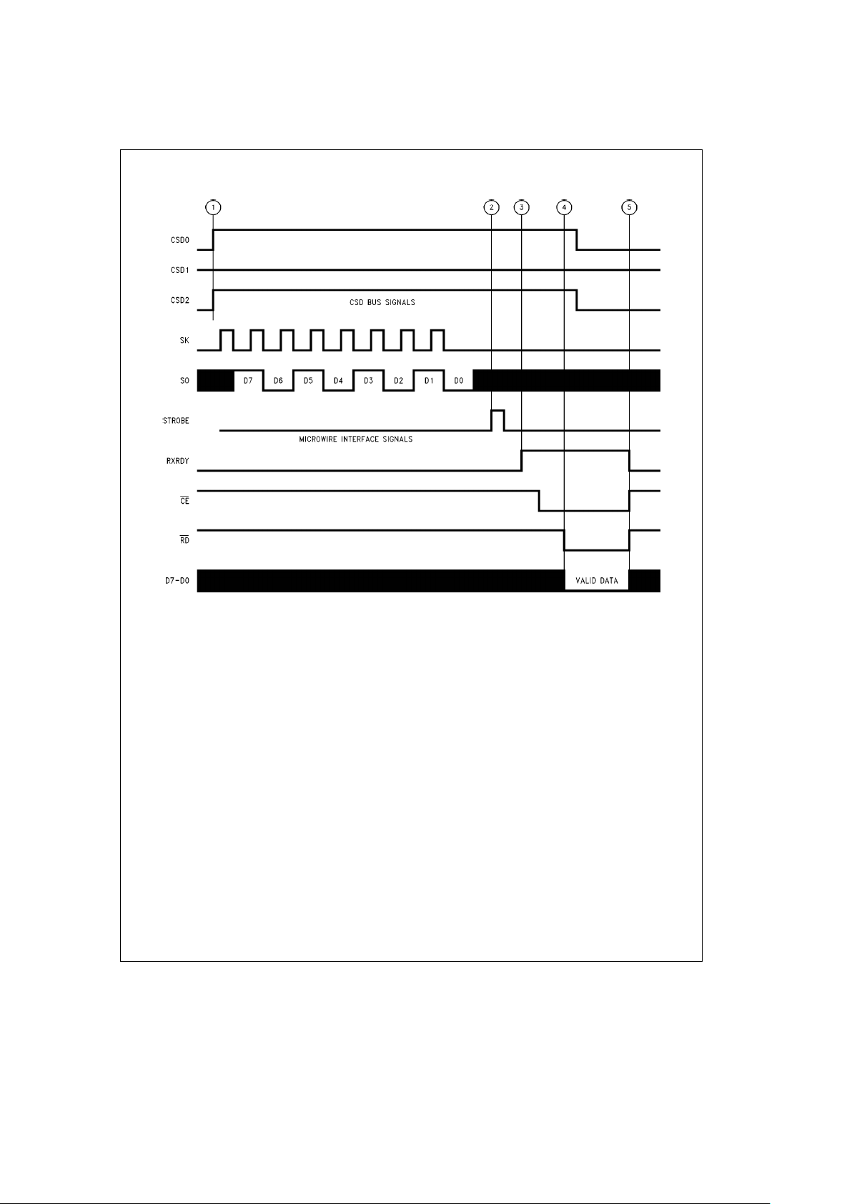
TL/DD/11727– 18
PARALLEL DATA BUS SIGNALS
FIGURE 13. Data Bus Read from Controller (ICSS1001) Write
25
Page 26
Data Transfer Timing (Continued)
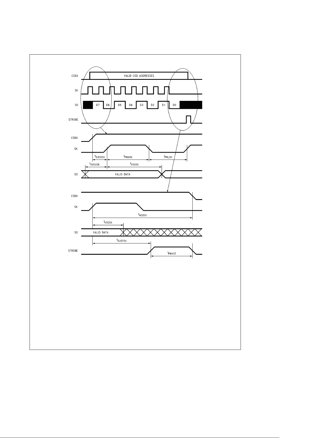
TL/DD/11727– 19
FIGURE 14. MICROWIRE Interface: Controller (ICSS1001) Write to Digital Chip (ICSS1002)
26
Page 27
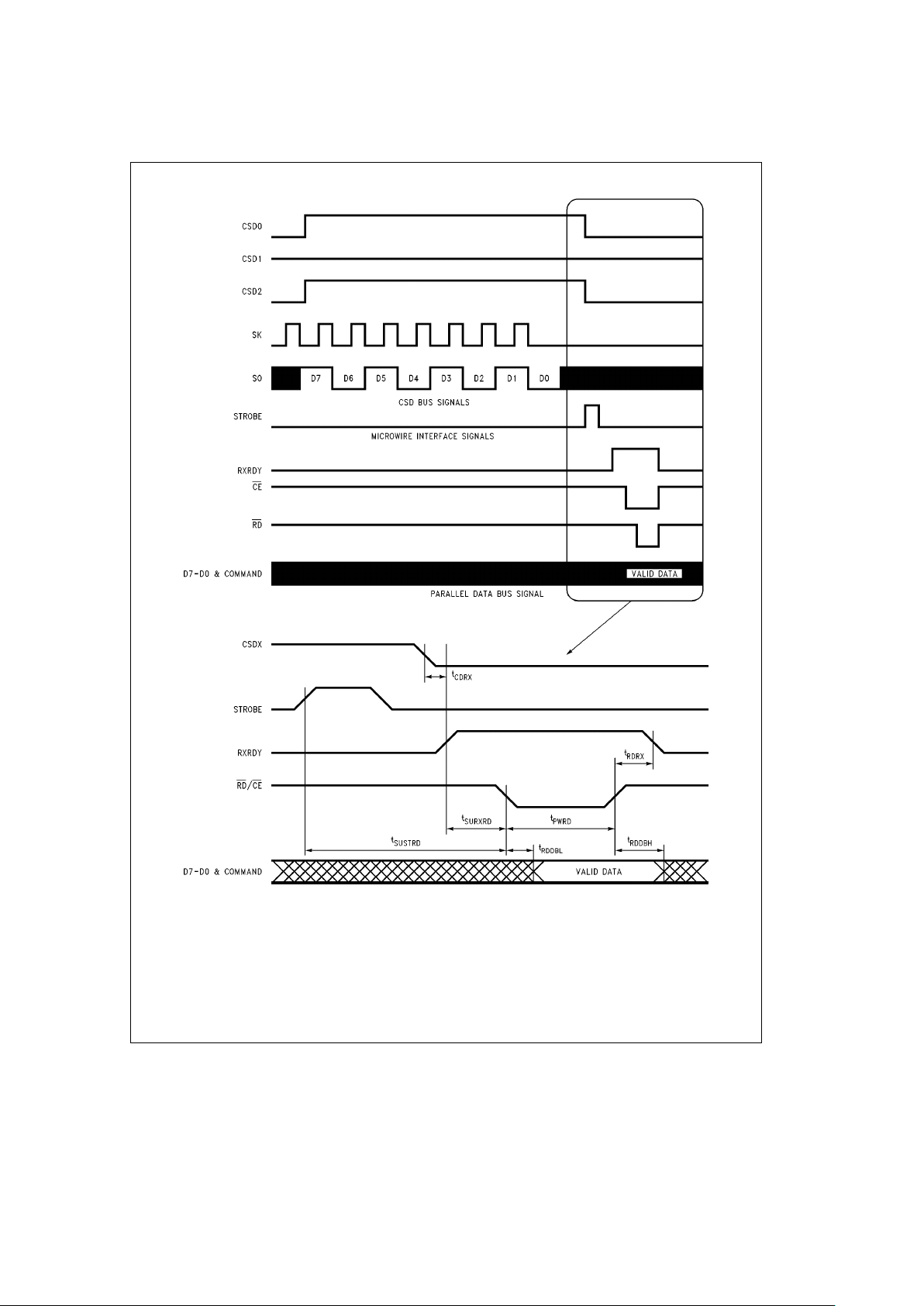
Data Transfer Timing (Continued)
TL/DD/11727– 20
FIGURE 15. Host Port Read from Digital Chip (ICSS1002)
27
Page 28
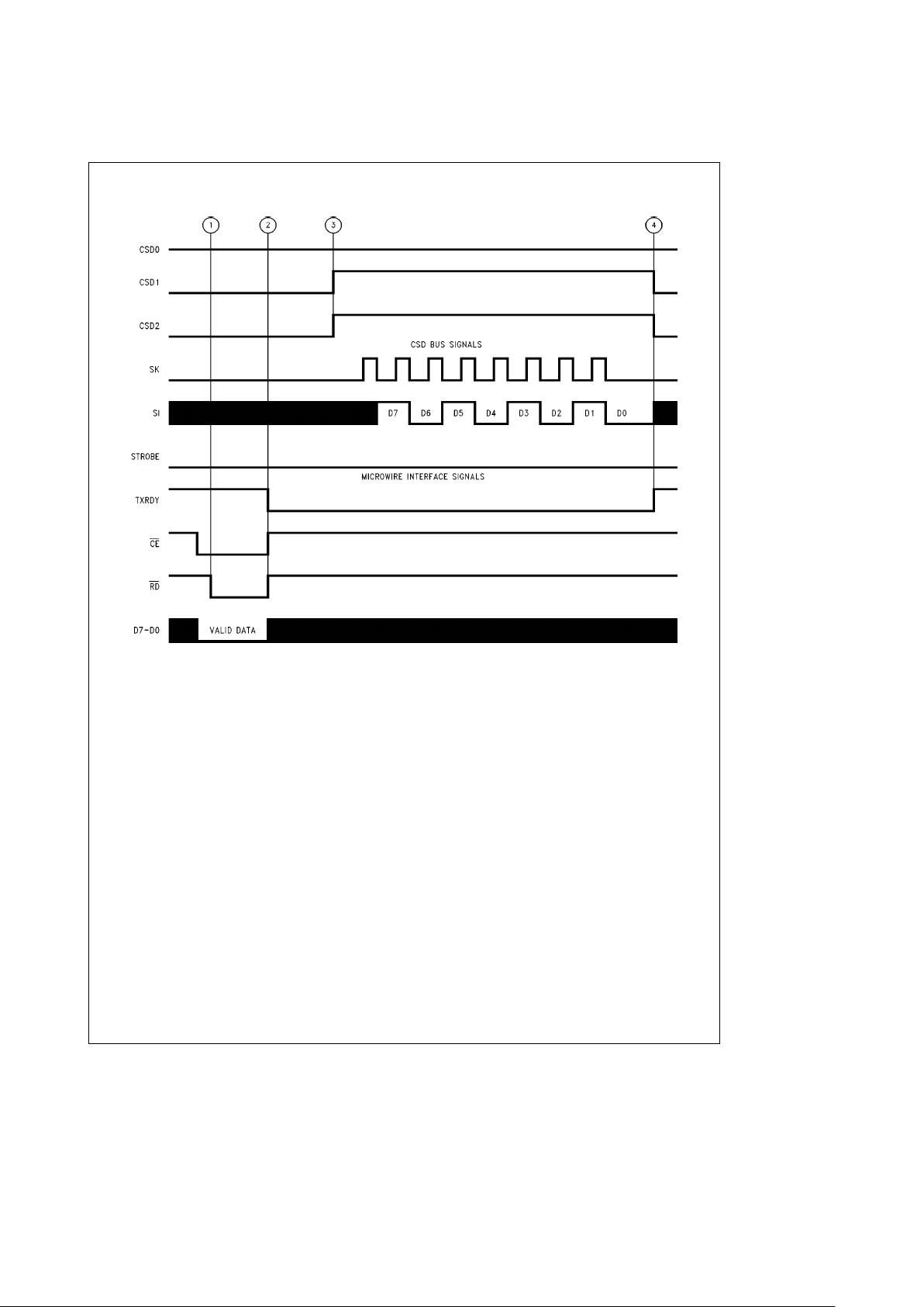
Data Transfer Timing (Continued)
TL/DD/11727– 21
PARALLEL DATA BUS SIGNALS
FIGURE 16. Controller (ICSS1001) Read from Data Bus Write
28
Page 29
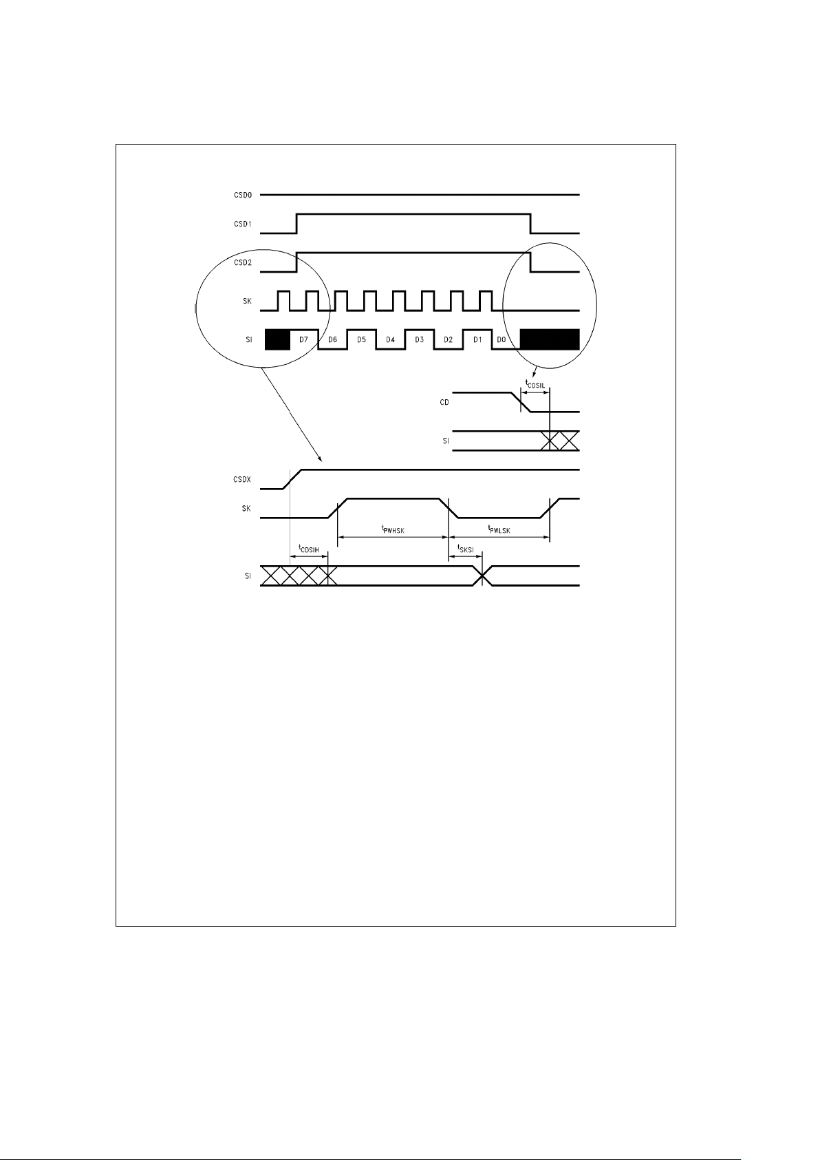
Data Transfer Timing (Continued)
TL/DD/11727– 22
FIGURE 17. MICROWIRE Interface: Controller (ICSS1001) Read from Digital Chip (ICSS1002)
29
Page 30
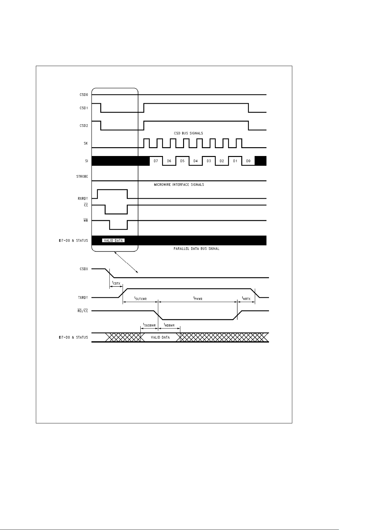
Data Transfer Timing (Continued)
TL/DD/11727– 23
FIGURE 18. Host Write to Digital Chip (ICSS1002)
30
Page 31
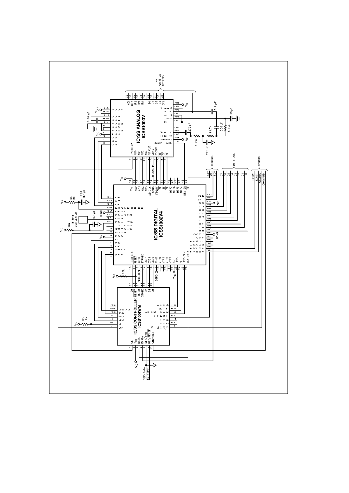
System Configurations
TL/DD/11727– 24
FIGURE 19. IC/SS Parallel Configuration
31
Page 32
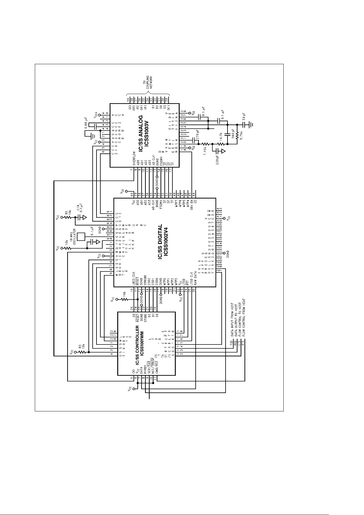
System Configurations (Continued)
TL/DD/11727– 25
FIGURE 20. IC/SS Serial Configuration
32
Page 33
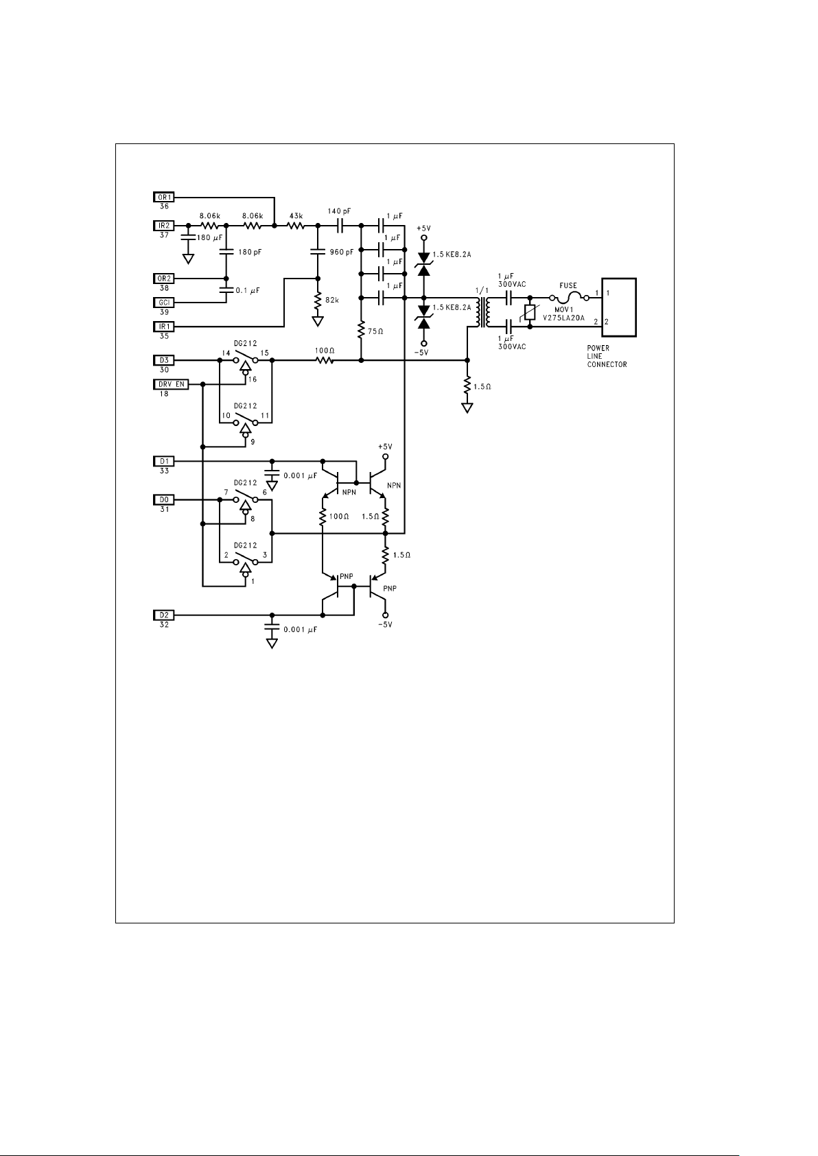
System Configurations (Continued)
TL/DD/11727– 26
FIGURE 21. Sample Coupling Network for IC/SS Chip Set
33
Page 34
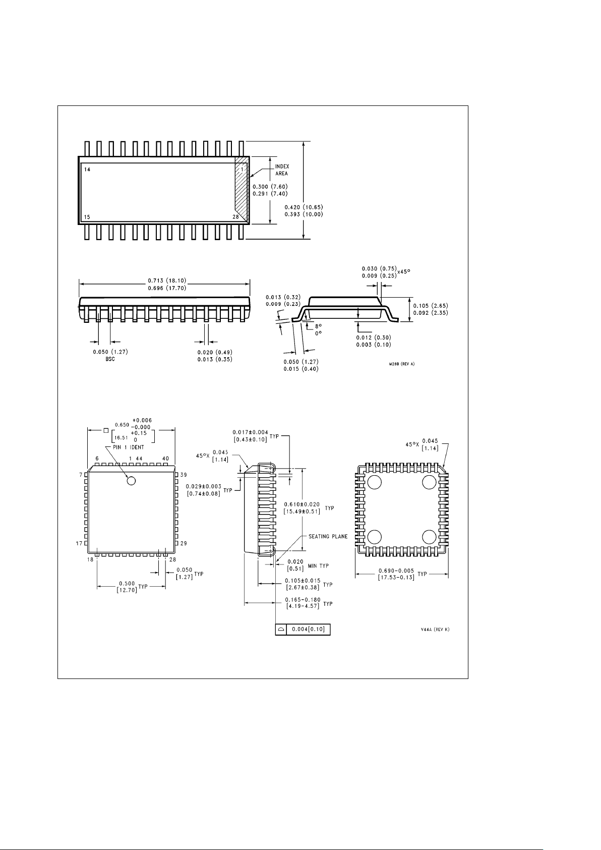
Physical Dimensions inches (millimeters)
Molded Small Outline Package (WM)
Order Number ICSS1001WM
NS Package Number M28B
Plastic Leaded Chip Carrier (PLCC)
Order Number ICSS1003V
NS Package Number V44A
34
Page 35
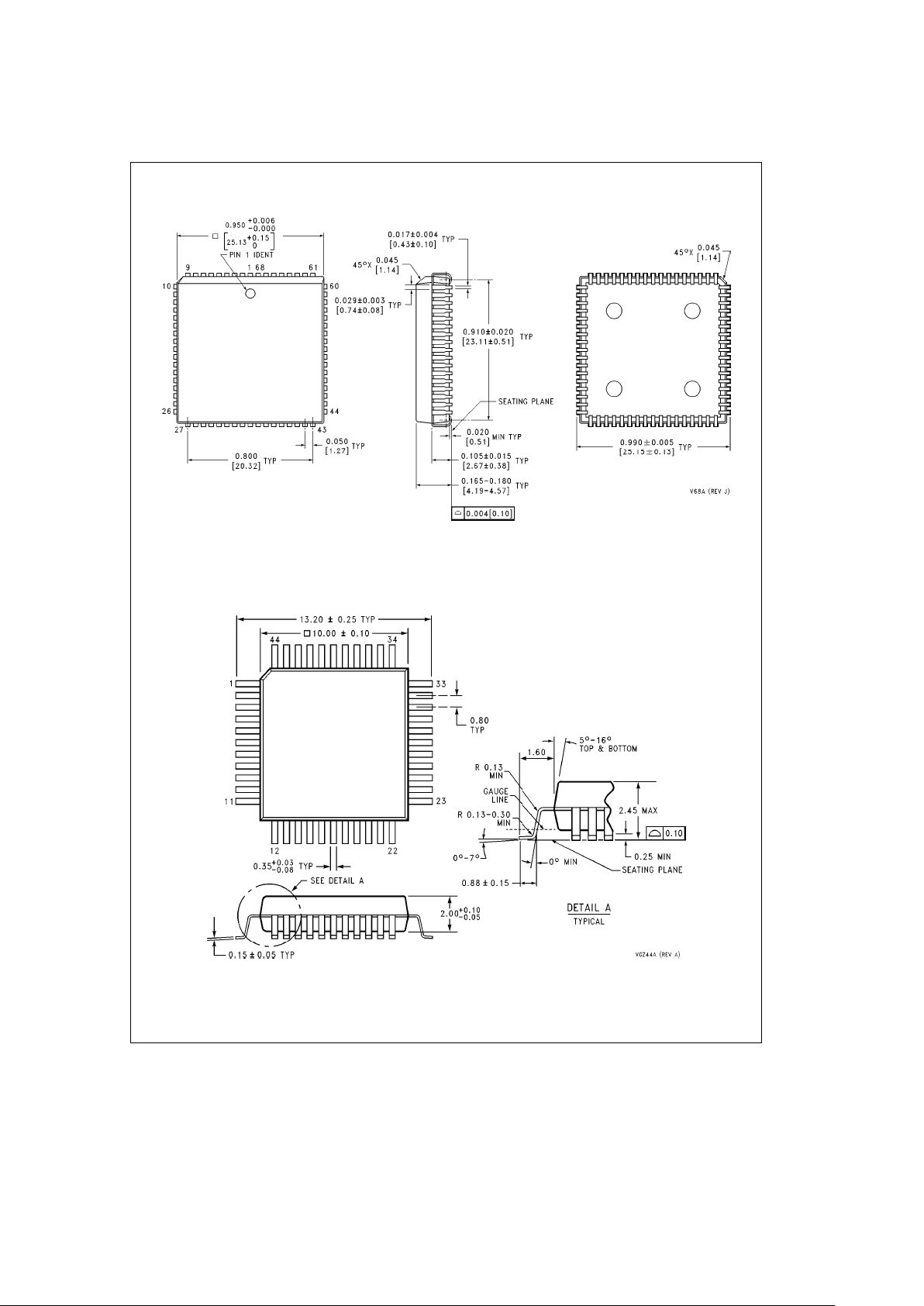
Physical Dimensions inches (millimeters) (Continued)
Plastic Leaded Chip Carrier (PLCC)
Order Number ICSS1002V4
NS Package Number V68A
Plastic Quad Flatpak (PQFP)
Order Number ICSS1003VGZ
NS Package Number VGZ44A
35
Page 36
ICSS1001, ICSS1002, and ICSS1003 IC/SS Power Line Carrier Local Area Network Chip Set
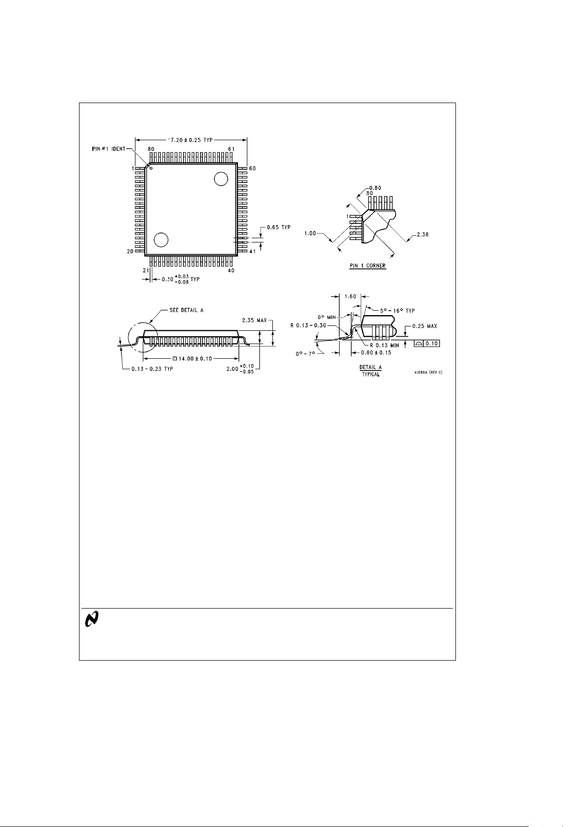
Physical Dimensions inches (millimeters) (Continued)
Plastic Quad Flatpak (PQFP)
Order Number ICSS1002VJE
NS Package Number VJE80A
LIFE SUPPORT POLICY
NATIONAL’S PRODUCTS ARE NOT AUTHORIZED FOR USE AS CRITICAL COMPONENTS IN LIFE SUPPORT
DEVICES OR SYSTEMS WITHOUT THE EXPRESS WRITTEN APPROVAL OF THE PRESIDENT OF NATIONAL
SEMICONDUCTOR CORPORATION. As used herein:
1. Life support devices or systems are devices or 2. A critical component is any component of a life
systems which, (a) are intended for surgical implant support device or system whose failure to perform can
into the body, or (b) support or sustain life, and whose be reasonably expected to cause the failure of the life
failure to perform, when properly used in accordance support device or system, or to affect its safety or
with instructions for use provided in the labeling, can effectiveness.
be reasonably expected to result in a significant injury
to the user.
National Semiconductor National Semiconductor National Semiconductor National Semiconductor
Corporation Europe Hong Kong Ltd. Japan Ltd.
1111 West Bardin Road Fax: (
a
49) 0-180-530 85 86 13th Floor, Straight Block, Tel: 81-043-299-2309
Arlington, TX 76017 Email: [email protected] Ocean Centre, 5 Canton Rd. Fax: 81-043-299-2408
Tel: 1(800) 272-9959 Deutsch Tel: (
a
49) 0-180-530 85 85 Tsimshatsui, Kowloon
Fax: 1(800) 737-7018 English Tel: (
a
49) 0-180-532 78 32 Hong Kong
Fran3ais Tel: (
a
49) 0-180-532 93 58 Tel: (852) 2737-1600
Italiano Tel: (
a
49) 0-180-534 16 80 Fax: (852) 2736-9960
National does not assume any responsibility for use of any circuitry described, no circuit patent licenses are implied and National reserves the right at any time without notice to change said circuitry and specifications.
 Loading...