

Page 1
Integrated
2X
Circuit
Systems, Inc.
AMD - K8™ System Clock Chip
ICS950405
Recommended Application:
AMD K8 System Clock with AMD, VIA or ALI Chipset
Output Features:
• 2 - Differential pair push-pull CPU clocks @
3.3V
• 9 - PCICLK (Including 1 free running) @ 3.3V
• 3 - Selectable PCICLK/HTTCLK @ 3.3V
• 1 - HTTCLK @ 3.3V
• 1 - 48MHz @ 3.3V fixed.
• 1 - 24/48MHz @ 3.3V
• 3 - REF @ 3.3V, 14.318MHz.
Functionality
FS0FS3 FS2 FS1
0 0 0 0 100.90 67.27 33.63
0 0 0 1 133.90 66.95 33.48
0 0 1 0 168.00 67.20 33.60
0 0 1 1 202.00 67.33 33.67
0 1 0 0 100.20 66.80 33.40
0 1 0 1 133.50 66.75 33.38
0 1 1 0 166.70 66.68 33.34
0 1 1 1 200.40 66.80 33.40
1 0 0 0 150.00 60.00 30.00
1 0 0 1 180.00 60.00 30.00
1 0 1 0 210.00 70.00 35.00
1 0 1 1 240.00 60.00 30.00
1 1 0 0 270.00 67.50 33.75
1 1 0 1 233.33 66.67 33.33
1 1 1 0 266.67 66.67 33.33
1 1 1 1 300.00 75.00 37.50
CPU HTT PCI
MHz MHz MHz
*ModeB/PCICLK8/HTTCLK1 7 42 GND
Features:
• Programmable output frequency.
• Programmable output divider ratios.
• Programmable output rise/fall time.
• Programmable output skew.
• Programmable spread percentage for EMI control.
• Watchdog timer technology and RESET# output to
reset system
if system malfunctions.
• Programmable watch dog safe frequency.
• Support I
2
C Index read/write and block read/write
operations.
• Uses external 14.318MHz crystal.
• Supports Hyper Transport Technology (HTTCLK).
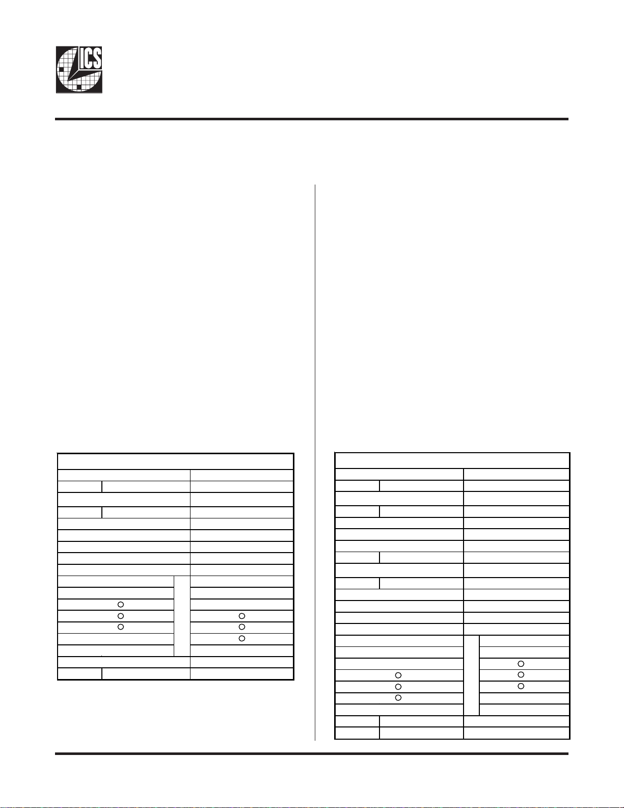
Pin Configur ation
*FS0/REF0 1 48 REF1/FS1*
VDDHTT 2 47 GND
X1 3 46 VDDREF
X2 4 45 REF2/FS2*
GND 5 44 Reset#
*ModeA/HTTCLK0 6 43 VDDA
PCICLK9/HTTCLK2 8 41 CPUCLK8T0
VDDPCI 9 40 CPUCLK8C0
GND 10 39 GND
PCICLK11/HTTCLK3 11 38 VDDCPU
PCICLK10 12 37 CPUCLK8T1
PCICLK013 36CPUCLK8C1
PCICLK114 35VDDCPU
GND 15 34 GND
VDDPCI 16 33 GND
PCICLK217 32PD#*
PCICLK3 18 31 48MHz/FS3**
VDDPCI 19 30 GND
GND 20 29 AVDD48
2X
PCICLK4
2X
PCICLK5
2X
PCICLK6
PCICLK7
21 28 24_48MHz/Sel24_48#*
22 27 GND
23 26 SDATA
24 25 SCLK
ICS950405
48-SSOP
2X
This Output has 2X Default Drive and can be programmaed lower via IIC
* Internal Pull-Up Resistor
0802F—04/22/05
Page 2
ICS950405
pply
y
y
p
p
p
p
pply
p
p
p
p
p
p
pply
p
p
pply
p
p
p
p
p
p
p
y
p
p
pply
p
p
pply
p
p
p
p
p
g
q
p
p
Pin Descriptions
PIN # PIN NAME
1
*FS0/REF0
VDDHTT
2
X1
3
X2
4
GND
5
*ModeA/HTTCLK0
6
*ModeB/PCICLK8/HTTCLK1
7
PCICLK9/HTTCLK2
8
VDDPCI
9
10 GND PWR Ground
PCICLK11/HTTCLK3
11
12 PCICLK10 OUT PCI clock out
PCICLK0
13
PCICLK1
14
GND
15
16 VDDPCI PWR Power su
17 PCICLK2 OUT PCI clock out
18 PCICLK3 OUT PCI clock out
VDDPCI
19
GND
20
21
2XPCICLK4
22
2XPCICLK5
23 2XPCICLK6 OUT
24 2XPCICLK7 OUT
25 SCLK IN Clock
26 SDATA I/O Data
27 GND PWR Ground
28 24_48MHz/Sel24_48#* I/O 24/48MHz clock output / Latched select input for 24/48MHz output. 0=48MHz, 1 = 24MHz.
29 AVDD48 PWR Power for 24/48MHz out
30 GND PWR Ground
31 48MHz/FS3** I/O Fixed 48MHz clock out
32 PD#* IN
33 GND PWR Ground
34 GND PWR Ground
35 VDDCPU PWR Su
36 CPUCLK8C1 OUT Com
37 CPUCLK8T1 OUT True clock of differential 3.3V
38 VDDCPU PWR Su
39 GND PWR Ground
40 CPUCLK8C0 OUT Com
41 CPUCLK8T0 OUT True clock of differential 3.3V
42 GND PWR Ground
43 VDDA PWR 3.3V
44 Reset# OUT
45 REF2/FS2* I/O 14.318 MHz reference clock / Fre
46 VDDREF PWR Ref, XTAL
47 GND PWR Ground
48 REF1/FS1* I/O 14.318 MHz reference clock / Frequency select latch input pin.
PIN
TYPE
I/O Frequency select latch input pin / 14.318 MHz reference clock.
PWR Su
IN Cr
OUT Cr
PWR Ground
I/O Mode selection latch in
I/O Mode selection latch in
OUT PCI clock out
PWR Power su
I/O PCI clock out
OUT PCI clock out
OUT PCI clock out
PWR Ground
PWR Power su
PWR Ground
OUT
OUT
for HTT clocks, nominal 3.3V.
stal input, Nominally 14.318MHz.
stal output, Nominally 14.318MHz
in.
ut / Hyper Transport output.
for PCI clocks, nominal 3.3V
in.
ut / Hyper Transport output.
ut.
ut.
ut.
in.
for PCI clocks, nominal 3.3V
ut.
ut.
for PCI clocks, nominal 3.3V
PCI clock output. This output is default @ 2X drive and can be programmed to lower drive
via IIC.
PCI clock output. This output is default @ 2X drive and can be programmed to lower drive
via IIC.
PCI clock output. This output is default @ 2X drive and can be programmed to lower drive
via IIC.
PCI clock output. This output is default @ 2X drive and can be programmed to lower drive
via IIC.
Asynchronous active low input pin used to power down the device into a low power state.
The internal clocks are disabled and the VCO and the cr
Real time system reset signal for frequency gear ratio change or watchdog timer timeout.
This si
in.
in of I2C circuitry 5V tolerant
in for I2C circuitry 5V tolerant
in.
in.
in.
in.
for CPU clocks, 3.3V nominal
limentary clock of differential 3.3V push-pull K8 pair.
for CPU clocks, 3.3V nominal
in.
limentary clock of differential 3.3V push-pull K8 pair.
in.
ower for the PLL core.
nal is active low.
ower supply, nominal 3.3V
in.
ut pin / Hyper Transport output.
ut pin / PCI clock output / Hyper Transport output.
uts and fixed PLL core, nominal 3.3V
ut. 3.3V / 'Frequency select latch input pin
* Internal Pull-Up Resistor ** Internal Pull-Down Resistor ~ 1.5X Drive Strength
0802F—04/22/05
DESCRIPTION
stal are stopped.
ush-pull K8 pair.
ush-pull K8 pair.
uency select latch input pin.
2
Page 3
ICS950405
General Description
The ICS950405 is a main system clock solution for desktop designs using the AMD K8 CPU. It provides all necessary
clock signals for Clawhammer and Sledgehammer with AMD, VIA or ALI systems.
The ICS950405 is part of a whole new line of ICS clock generators and buffers called TCH™ (Timing Control Hub). This
part incorporates ICS's newest clock technology which offers more robust features and functionality. Employing the
use of a serially programmable I
setting, the output divider ratios, selecting the ideal spread percentage, the output skew, the output strength, and
enabling/disabling each individual output clock. M/N control can configure output frequency with resolution up to
0.1MHz increment.
Block Diagram
2
C interface, this device can adjust the output clocks by configuring the frequency
X1
X2
PD#
SDATA
SCLK
FS (3:0)
MODE (A,B)
PLL2
XTAL
OSC
PLL1
Spread
Spectr
Control
Logic
Config.
Reg.
um
CPU
DIVDER
PCI
DIVDER
HTT
DIVDER
/ 2
48MHz
24_48MHz
REF (2:0)
CPUCLKC (1:0)
CPUCLKT (1:0)
PCICLK (7:0, 10)
PCICLK(11,9,8)/HTTCLK (3:1)
HTTCLK0
SEL24_48#
0802F—04/22/05
3
Page 4
ICS950405
Power Groups
Pin Number
VDD GND
2 5 Xtal, POR
9 10 PCICLK, HTTCLK O/p
16,19 15,20 PCICLK Outputs
29 27,30,33 48 MHz, Fix Analog
35,38 34,39 CPU Outputs
43 42 Analog, CPU PLL, MCLK
46 47 REF, Digital Core
Description
Mode Functionality Tables
ModeA ModeB Pin7 Pin8 Pin11
0 0 HTTCLK1 HTTCLK2 PCICLK11
0 1 HTTCLK1 HTTCLK2 HTTCLK3
1 0 PCICLK8 PCICLK9 PCICLK11
1 1 HTTCLK1 PCICLK9 PCICLK11
Table1: Frequency Selection Table
Bit3 Bit2 Bit1 Bit0
FS3 FS2 FS1 FS0 MHz MHz MHz
000 0
000 1
001 0
001 1
0 1 0 0 100.20 66.80 33.40
010 1
011 0
011 1
100 0
100 1
101 0
101 1
110 0
110 1
111 0
111 1
CPU HTT PCI
100.90 67.27 33.63
133.90 66.95 33.48
168.00 67.20 33.60
202.00 67.33 33.67
133.50 66.75 33.38
166.70 66.68 33.34
200.40 66.80 33.40
150.00 60.00 30.00
180.00 60.00 30.00
210.00 70.00 35.00
240.00 60.00 30.00
270.00 67.50 33.75
233.33 66.67 33.33
266.67 66.67 33.33
300.00 75.00 37.50
0802F—04/22/05
4
Page 5
General I2C serial interface information
ICS950405
How to Write:
• Controller (host) sends a start bit.
• Controller (host) sends the write address D2
• ICS clock will
acknowledge
• Controller (host) sends the begining byte location = N
• ICS clock will
acknowledge
• Controller (host) sends the data byte count = X
• ICS clock will
• Controller (host) starts sending
acknowledge
Byte N through
Byte N + X -1
(see Note 2)
• ICS clock will
acknowledge
each byte
• Controller (host) sends a Stop bit
Index Block Write Operation
Controller (Host)
T
Slave Address D2
WR
Beginning Byte = N
Data Byte Count = X
Beginning Byte N
starT bit
WRite
(H)
ICS (Slave/Receiver)
ACK
ACK
ACK
ACK
(H)
one at a time
How to Read:
• Controller (host) will send start bit.
• Controller (host) sends the write address D2
• ICS clock will
acknowledge
• Controller (host) sends the begining byte
location = N
• ICS clock will
acknowledge
• Controller (host) will send a separate start bit.
• Controller (host) sends the read address D3
• ICS clock will
acknowledge
• ICS clock will send the data byte count = X
• ICS clock sends
• ICS clock sends
was written to byte 8)
Byte N + X -1
Byte 0 through byte X (if X
.
• Controller (host) will need to acknowledge each byte
• Controllor (host) will send a not acknowledge bit
• Controller (host) will send a stop bit
Index Block Read Operation
Controller (Host)
T starT bit
Slave Address D2
WR WRite
Beginning Byte = N
RT Repeat starT
Slave Address D3
RD ReaD
(H)
(H)
ICS (Slave/Receiver)
ACK
ACK
ACK
(H)
(H)
(H)
Byte N + X - 1
P
0802F—04/22/05
stoP bit
X Byte
ACK
N Not acknowledge
PstoP bit
ACK
ACK
Data Byte Count = X
Beginning Byte N
X Byte
Byte N + X - 1
5
Page 6
ICS950405
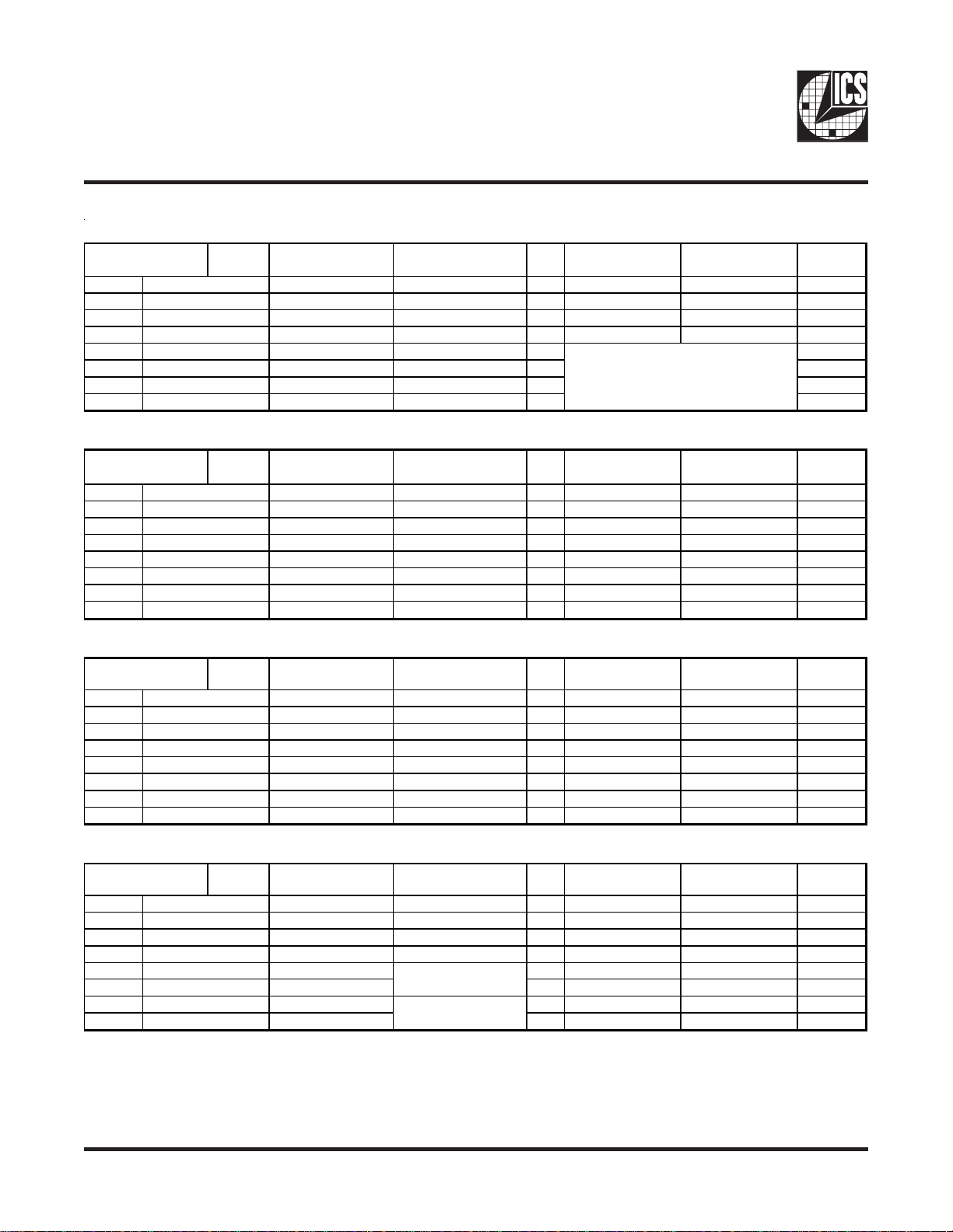
I2C Table: Frequency Select Register
Bit 7
Bit 6
Bit 5
Bit 4
Bit 3
Bit 2
Bit 1
Bit 0
- OFF ON
- 48MHz 24MHz
- Reserved Reser ved
- Reserved Reser ved
-
-
-
-
I2C Table: Output Control Register
Bit 7
Bit 6
Bit 5
Bit 4
Bit 3
Bit 2
Bit 1
Bit 0
1 Disable Enable
6 Disable Enable
7 Disable Enable
8 Disable Enable
11 Disable Enable
12 Disable Enable
13 Disable Enable
14 Disable Enable
SS_EN Spread Enable RW 1
SEL24_48MHz Output Select RW Latch
Reserved Reserved RW X
Reserved Reserved RW X
FS3 Fr eq Select Bit 3 RW Latch
FS2 Fr eq Select Bit 2 RW Latch
FS1 Fr eq Select Bit 1 RW Latch
FS0 Fr eq Select Bit 0 RW Latch
REF0 Output Control RW 1
HTTCLK0 Output Control RW 1
PCICLK8/HTTCLK1 Output Control RW 1
PCICLK9/HTTCLK2 Output Control RW 1
PCICLK11/HTTCLK3 Output Control RW 1
PCICLK10 Output Control RW 1
PCICLK0 Output Control RW 1
PCICLK1 Output Control RW 1
Type 0 1
See Table1: Frequency Selection Table
Type 0 1 PWDByte 1 Pin # Name Control Function
PWDByte 0 Pin # Name Control Function
I2C Table: Output Control Register
Bit 7
Bit 6
Bit 5
Bit 4
Bit 3
Bit 2
Bit 1
Bit 0
17 Disable Enable
18 Disable Enable
21 Disable Enable
22 Disable Enable
23 Disable Enable
24 Disable Enable
28 Disable Enable
31 Disable Enable
PCICLK2 Output Control RW 1
PCICLK3 Output Control RW 1
PCICLK4 Output Control RW 1
PCICLK5 Output Control RW 1
PCICLK6 Output Control RW 1
PCICLK7 Output Control RW 1
24_48MHz Output Control RW 1
I2C Table: Output Control Register
Bit 7
Bit 6
Bit 5
Bit 4
Bit 3
Bit 2
Bit 1
Bit 0
37,36 Disable Enable
41,40 Disable Enable
45 Disable Enable
48 Disable Enable
- 00: 0.5X Drive 10: 1.5X Drive
- 01: 1.0X Drive 11: 2.0X Drive
- 00: 0.5X Drive 10: 1.5X Drive
- 01: 1.0X Drive 11: 2.0X Drive
CPUCLK8T/C_1 Output Control RW 1
CPUCLK8T/C_0 Output Control
PCI_Str1
PCI_Str0
PCI_Str1
PCI_Str0
Type 0 1 PWDByte 2 Pin # Name Control Function
48MHz Output Control RW 1
Type 0 1 PWDByte 3 Pin # Name Control Function
RW 1
REF2 Output Control RW 1
REF1 Output Control
PCI9,8 Strength
Control only
PCI11 Strength Control
only
RW 1
RW 0
RW 1
RW 0
RW 1
0802F—04/22/05
6
Page 7
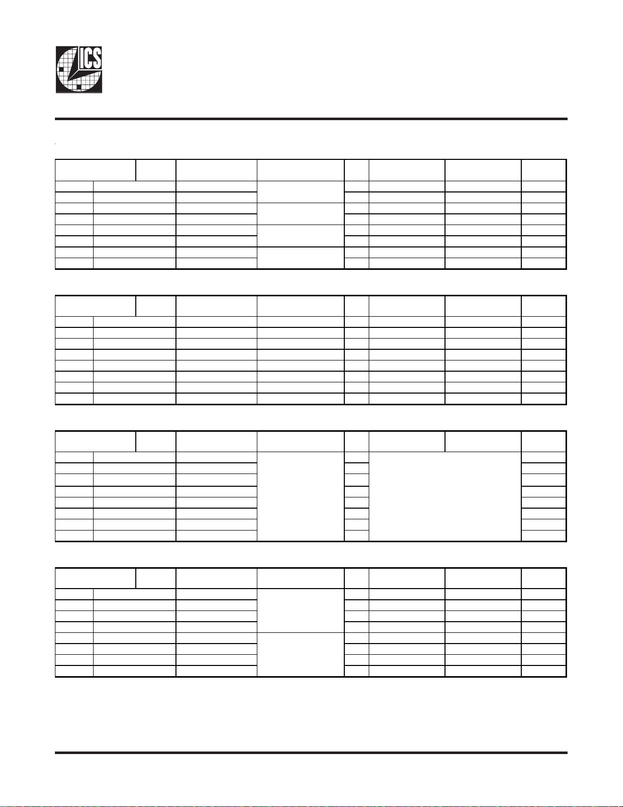
I2C Table: Output Control Register
Bit 7
Bit 6
Bit 5
Bit 4
Bit 3
Bit 2
Bit 1
Bit 0
-
-
-
-
-
-
-
-
PCIStr1
PCIStr0
PCIStr1
PCIStr0
PCIStr1
PCIStr0
PCIStr1
PCIStr0
I2C Table: Reserved Register
Bit 7
Bit 6
Bit 5
Bit 4
Bit 3
Bit 2
Bit 1
Bit 0
-
-
-
-
-
-
-
-
Reserved Reserved RW X
Reserved Reserved RW X
Reserved Reserved RW X
Reserved Reserved RW X
Reserved Reserved RW X
Reserved Reserved RW X
Reserved Reserved RW X
Reserved Reserved RW X
All other PCICLK
Strength Control
PCICLK (7:6) Strength
Control
PCICLK (5) Strength
Control
PCICLK (4) Strength
Control
ICS950405
Type 0 1 PWDByte 4 Pin # Name Control Function
RW 0
RW 1
RW 1
RW 1
RW 1
RW 1
RW 1
RW 1
Type 0 1
00: 0.5X Drive 10: 1.5X Drive
01: 1.0X Drive 11: 2.0X Drive
00: 0.5X Drive 10: 1.5X Drive
01: 1.0X Drive 11: 2.0X Drive
00: 0.5X Drive
01: 1.0X Drive 11: 2.0X Drive
00: 0.5X Drive 10: 1.5X Drive
01: 1.0X Drive 11: 2.0X Drive
Reserved Reserved
Reserved
Reserved Reserved
Reserved
Reserved Reserved
Reserved Reserved
Reserved Reserved
Reserved Reserved
10: 1.5X Drive
Reserved
Reserved
PWDByte 5 Pin # Name Control Function
I2C Table: Byte Count Register
Bit 7
Bit 6
Bit 5
Bit 4
Bit 3
Bit 2
Bit 1
Bit 0
-
-
-
-
-
-
-
-
BC7 RW 0
BC6 RW 0
BC5 RW 0
BC4 RW 0
BC3 RW 0
BC2 RW 1
BC1 RW 1
BC0 RW 0
I2C Table: Byte Count and Vendor ID Register
Bit 7
Bit 6
Bit 5
Bit 4
Bit 3
Bit 2
Bit 1
Bit 0
- --
- --
- --
- --
- --
- --
- --
- --
REV_ID3 RW 0
REV_ID2 RW 0
REV_ID1 RW 0
REV_ID0 RW 0
Vendor_ID3 RW 0
Vendor_ID2 RW 0
Vendor_ID1 RW 0
Vendor_ID0 RW 1
Byte Count
Programming b(7:0)
Revision ID
Vendor ID
Type 0 1 PWDByte 6 Pin # Name Control Function
Writing to this register will c onfigur e how
many bytes will be read bac k, default is
06 = 6 bytes.
Type 0 1 PWDByte 7 Pin # Name Control Function
0802F—04/22/05
7
Page 8
ICS950405
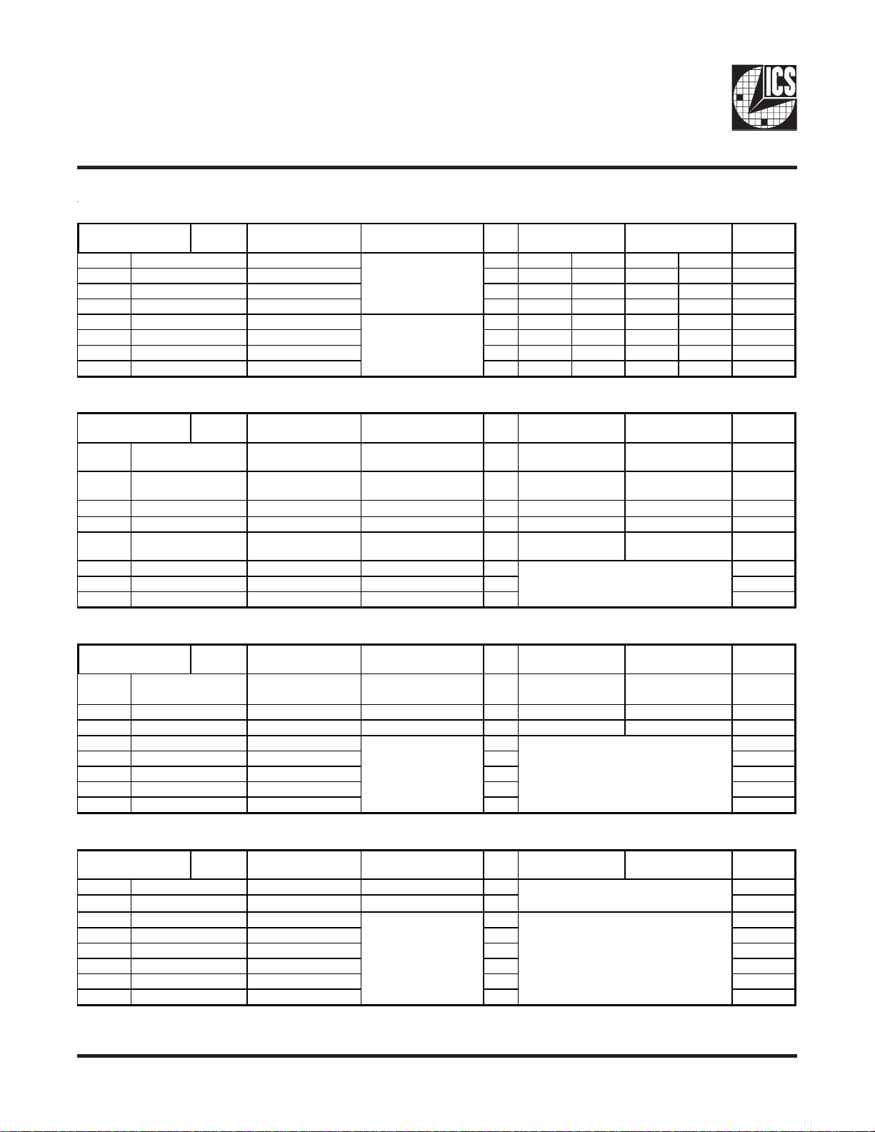
I2C Table: Skew Control Register
Bit 7
Bit 6
Bit 5
Bit 4
Bit 3
Bit 2
Bit 1
Bit 0
-
-
-
-
-
-
-
-
I2C Table: WD Time Control & Async Frequency Selection Register
Bit 7
Bit 6
Bit 5
Bit 4
Bit 3
Bit 2
Bit 1
Bit 0
-
-
-
- --
- 290ms Base 1160ms Base
-
-
-
PCI/HTTSkw3 RW 0000:0 0100:150 1000:300 1100:450 1
PCI/HTTSkw2 RW 0001:N/A 0101:N/A 1001:N/A 1101:600 1
PCI/HTTSkw1 RW 0010:N/A 0110:N/A 1010:N/A 1110:750 0
PCI/HTTSkw0 RW 0011:N/A 0111:N/A 1011:N/A 1111:900 0
PCISkw3 RW 0000:0 0100:150 1000:300 1100:450 1
PCISkw2 RW 0001:N/A 0101:N/A 1001:N/A 1101:600 1
PCISkw1 RW 0010:N/A 0110:N/A 1010:N/A 1110:750 0
PCISkw0 RW 0011:N/A 0111:N/A 1011:N/A 1111:900 0
ASEL
AEN
Reserved Reserved RW X
Reserved Reserved RW X
WDTCtr l
WD2 WD Timer Bit 2 RW 1
WD1 WD Timer Bit 1 RW 1
WD0 WD Timer Bit 0 RW 1
CPU-PCI/HTT 7 Step
Skew Control (ps)
CPU-PCI 7 Step Skew
Control (ps)
Async Fr equency
Select
AGP/PCI/ Freq Sourc e
Select
Watch Dog Time base
Control
Type 0 1 PWDByte 8 Pin # Name Control Function
Type 0 1 PWDByte 9 Pin # Name Control Function
RW 0
RW 1
RW 0
66MHz 75.4MHz
FIX PLL CPU PLL
--
These bits represent X*290ms (or 1.16S)
the watchdog timer waits before it goes to
alarm mode. Default is 7 X 290ms = 2s.
I2C Table: VCO Control Select Bit & WD Timer Control Register
Bit 7
Bit 6
Bit 5
Bit 4
Bit 3
Bit 2
Bit 1
Bit 0
- Disable Enable
- Disable Enable
- Normal Alarm
-
-
-
-
-
M/NEN
WDEN Watc hdog Enable RW 0
WDStatus WD Alarm Status R 0
WD SF4 RW 0
WD SF3 RW 0
WD SF2 RW 0
WD SF1 RW 0
WD SF0 RW 0
M/N Programming
Enable
Watch Dog Safe Freq
Programming bits
I2C Table: VCO Frequency Control Register
Bit 7
Bit 6
Bit 5
Bit 4
Bit 3
Bit 2
Bit 1
Bit 0
0802F—04/22/05
-
-
-
-
-
-
-
-
N Div8 N Divider Prog bit 8 RW X
N Div9 N Divider Prog bit 9 RW X
M Div5 RW X
M Div4 RW X
M Div3 RW X
M Div2 RW X
M Div1 RW X
M Div0 RW X
M Divider Programming
bits (5:0)
1PWDByte 10 Pin # Name Control Function Type 0
RW 0
Writing to thes e bit will configure the safe
frequency as Byte0 bit (4:0).
Type 0 1
The decimal representation of N Divider in
Byte 11 and 12
The decimal representation of M and N
Div ier in Byte 11 and 12 will c onfigure the
VCO frequenc y. Default at power up =
latch-in or Byte 0 Rom table.
VCO Frequency = 14.318 x [NDiv(9:0)+8]
/ [MDiv(5:0)+2]
PWDByte 11 Pin # Name Control Function
8
Page 9
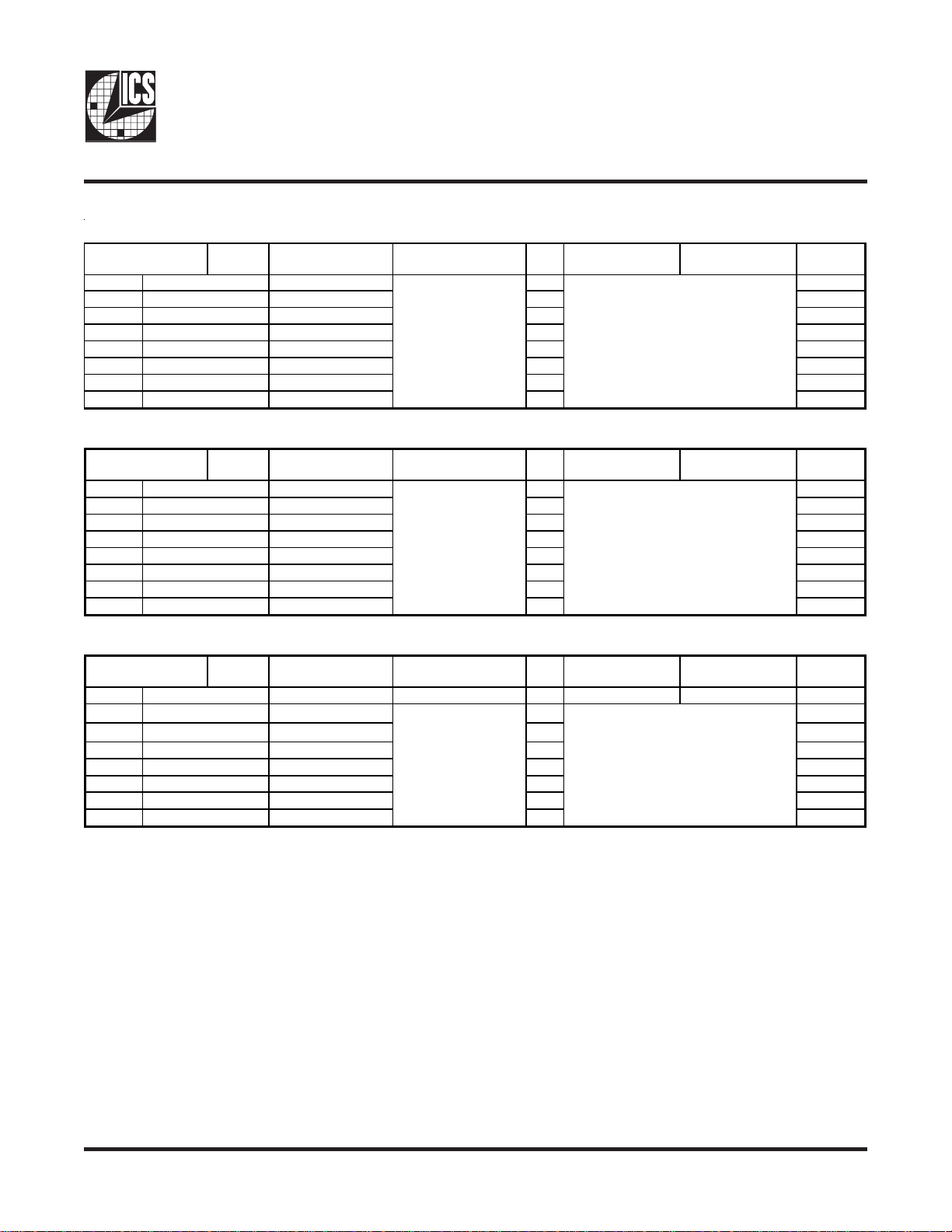
I2C Table: VCO Frequency Control Register
Bit 7
Bit 6
Bit 5
Bit 4
Bit 3
Bit 2
Bit 1
Bit 0
-
-
-
-
-
-
-
-
N Div7 RW X
N Div6 RW X
N Div5 RW X
N Div4 RW X
N Div3 RW X
N Div2 RW X
N Div1 RW X
N Div0 RW X
I2C Table: Spread Spectrum Control Register
Bit 7
Bit 6
Bit 5
Bit 4
Bit 3
Bit 2
Bit 1
Bit 0
-
-
-
-
-
-
-
-
SSP7 RW X
SSP6 RW X
SSP5 RW X
SSP4 RW X
SSP3 RW X
SSP2 RW X
SSP1 RW X
SSP0 RW X
N Divider Programming
bit (7:0)
Spread Spectrum
Programming b(7:0)
ICS950405
Type 0 1
The decimal representation of M and N
Div ier in Byte 11 and 12 will c onfigure the
VCO frequenc y. Default at power up =
latch-in or Byte 0 Rom table.
VCO Frequency = 14.318 x [NDiv(9:0)+8]
/ [MDiv(5:0)+2]
Type
0
These Spread Spectrum bits in Byte 13
and 14 will progr am the s pr ead
pecentage. It is recommended to us e
ICS Spread % table for spread
programming.
PWDByte 12 Pin # Name Control Function
1
PWDByte 13 Pin # Name Control Function
I2C Table: Spread Spectrum Control Register
Bit 7
Bit 6
Bit 5
Bit 4
Bit 3
Bit 2
Bit 1
Bit 0
- -
-
-
-
-
-
-
-
Reserved Reserved R 0
SSP14 RW X
SSP13 RW X
SSP12 RW X
SSP11 RW X
SSP10 RW X
SSP9 RW X
SSP8 RW X
Spread Spectrum
Programming b(14:8)
Type 0 1
These Spread Spectrum bits in Byte 13
and 14 will progr am the s pr ead
pecentage. It is recommended to us e
ICS Spread % table for spread
programming.
PWDByte 14 Pin # Name Control Function
-
0802F—04/22/05
9
Page 10
ICS950405
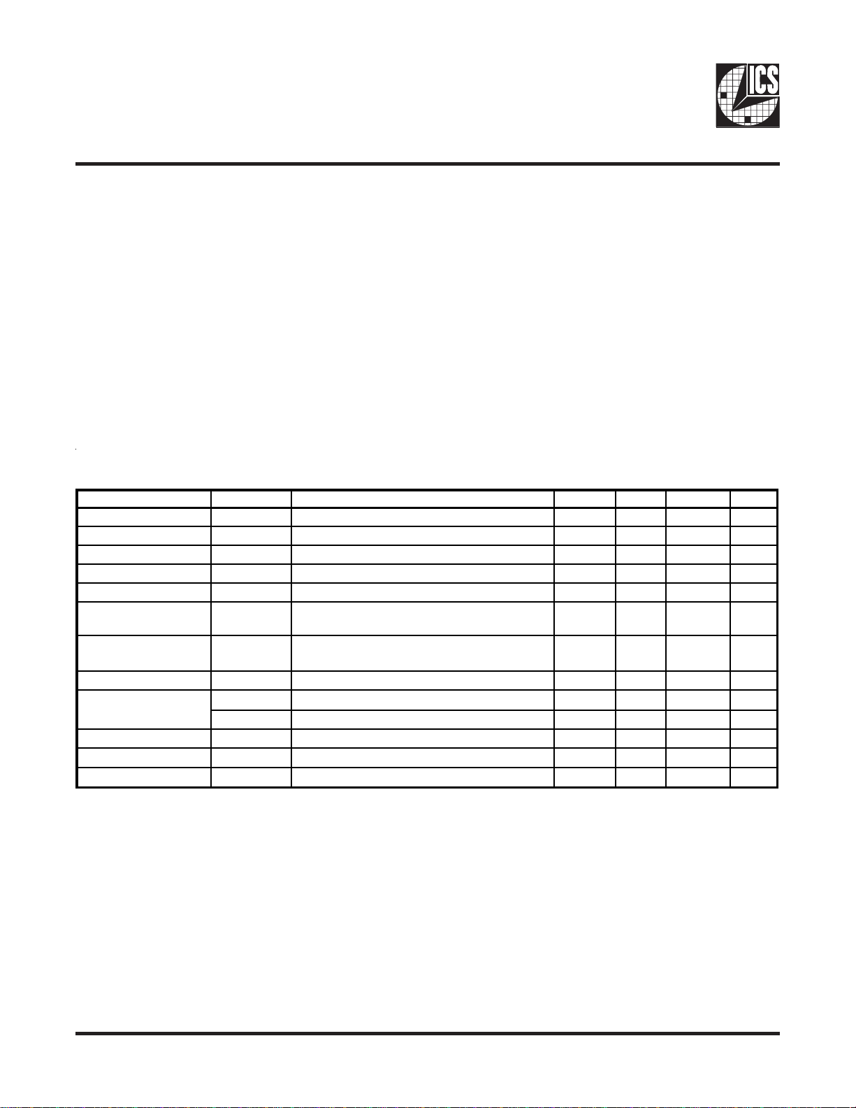
Absolute Maximum Ratings
Supply Voltage . . . . . . . . . . . . . . . . . . . . . . . . . 3.8V
Logic Inputs . . . . . . . . . . . . . . . . . . . . . . . . . . . GND –0.5 V to V
Ambient Operating Temperature . . . . . . . . . . 0°C to +70°C
Storage Temperature . . . . . . . . . . . . . . . . . . . . –65°C to +150°C
ESD Protection . . . . . . . . . . . . . . . . . . . . . . . . Input ESD protection usung human body model > 1KV
+3.8 V
DD
Stresses above those listed under
Absolute Maximum Ratings
may cause permanent damage to the device. These
ratings are stress specifications only and functional operation of the device at these or any other conditions above those
listed in the operational sections of the specifications is not implied. Exposure to absolute maximum rating conditions
for extended periods may affect product reliability.
Electrical Characteristics - Input/Supply/Common Output Parameters
TA = 0 - 70°C; Supply Voltage V
PARAMETER SYMBOL CONDITIONS MIN TYP MAX UNITS
Input High Voltage
Input Low Voltage
V
V
Input High Current
Input Low Current
Input Low Current
Operating Supply
Current
Power Down Supply
Current
I
I
I
DD(op)
I
DDPD
Input frequency
Input Capacitance
Transition Time
Clk Stabilization
1
Guaranteed by design, not 100% tested in production.
Skew
1
1
1
1
C
C
T
T
T
CPU-PCI
= 3.3 V +/-5% (unless otherwise stated)
DD
IH
IL
I
IH
IL1
IL2
VIN = V
DD
VIN = 0 V; Inputs with no pull-up resistors
VIN = 0 V; Inputs with pull-up resistors
CL = 0 pF; Select @ 100MHz
CL = 0 pF; With input address to Vdd or
GND
F
IN
INX
trans
STAB
VDD = 3.3 V;
i
Logic Inputs 5 pF
X1 & X2 pins 27 45 pF
To 1st crossing of target Freq. 3 ms
From VDD = 3.3 V to 1% target Freq.
VT = 1.5 V
+ 0.3
2
V
- 0.3
SS
V
DD
0.8 V
5mA
-5 mA
-200 mA
180 mA
40 mA
11 16 MHz
3ms
1.5 4 ns
V
0802F—04/22/05
10
Page 11
ICS950405
g
g
g
p
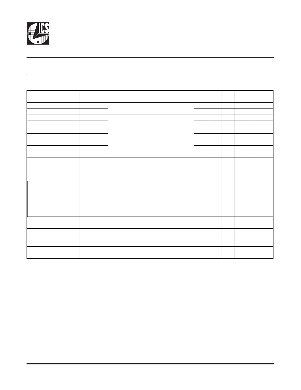
Electrical Characteristics - K8 Push Pull Differential Pair
TA = 0 - 70°C; V
PARAMETER SYMBOL CONDITIONS MIN TYP MAX UNITS NOTES
= 3.3 V +/-5%; CL =AMD64 Processor Test Load
DD
Edge Rate δV/δ
Risin
Edge Rate δV/δ
Fallin
Differential Voltage
Change in V
DIFF_DC
Magnitude
Common Mode Voltage
Change in Common
Mode Volta
e
V
DIFF
∆
V
DIFF
V
CM
∆
V
CM
Measured at the AMD64 processor's
t
test load. 0 V +/- 400 mV (differential
t
Measured at the AMD64 processor's
test load. (single-ended measurement)
210V/ns1
210V/ns1
0.4 2.3 V 1
-150 150 mV 1
1.05 1.45 V 1
-200 200 mV 1
Measurement from differential
Jitter, Cycle to cycle
t
jcyc-cyc
wavefrom. Maximum difference of cycle
0 200 ps 1
time between 2 adjacent cycles.
Measured using the JIT2 software
package with a Tek 7404 scope.
Jitter, Accumulated
t
ja
TIE (Time Interval Error) measurement
technique:
-1000 1000 1,2,3
Sample resolution = 50 ps,
le Duration = 10 µs
Sam
Duty Cycle
d
t3
Measurement from differential
wavefrom
45 53 % 1
Average value during switching
Output Impedance
R
ON
transition. Used for determining series
15 55
termination value.
Group Skew
1
Guaranteed by design and characterization, not 100% tested in production.
2
All accumulated jitter specifications are guaranteed assuming that REF is at 14.31818MHz
3
Spread Spectrum is off
t
src-skew
Measurement from differential
wavefrom
Ω
250 ps 1
1
0802F—04/22/05
11
Page 12
ICS950405
1
jcy
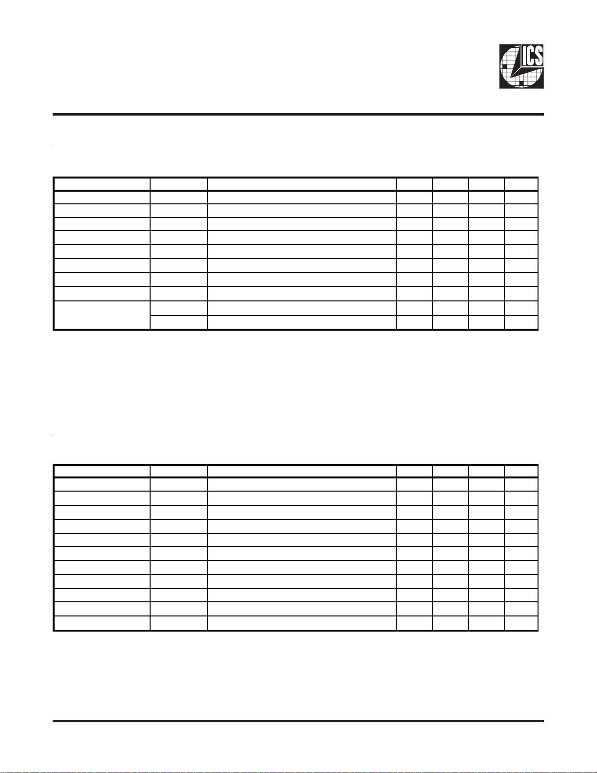
Electrical Characteristics - PCICLK
TA = 0 - 70°C; VDD = 3.3 V,+/-5%; CL = 30 pF
PARAMETER SYMBOL CONDITIONS MIN TYP MAX UNITS
Output High Voltage V
Output Low Voltage V
Output High Current I
Output Low Current I
Rise Time
Fall Time
Duty Cycle
Skew
1
1
1
1
Jitter
1
Guaranteed by design, not 100% tested in production.
OH1
OL1
OH1
OL1
t
r1
t
f1
d
t1
t
sk1
t
c-cyc
t
jabs1
IOH = -18 mA 2.1 V
IOL = 9.4 mA 0.4 V
VOH = 2.0 V -22 mA
VOL = 0.8 V 16 57 mA
VOL = 0.4 V, VOH = 2.4 V 2 ns
VOH = 2.4 V, VOL = 0.4 V 2 ns
VT = 1.5 V 45 55 %
VT = 1.5 V 500 ps
1
VT = 1.5 V 500 ps
VT = 1.5 V
500 ps
Electrical Characteristics - ZCLK
TA = 0 - 70°C; VDD=3.3V +/-5%; CL = 10-30 pF (unless otherwise specified)
PARAMETER SYMBOL CONDITIONS MIN TYP MAX UNITS
Output Frequency F
Output Impedance R
Output High Voltage V
Output Low Voltage V
Output High Current
Output Low Current
Rise Time t
Fall Time t
Duty Cycle
Skew t
Jitter
0802F—04/22/05
DSP1
OH
OL
I
OH
I
OL
r1
f1
d
sk1
t
jcyc-cyc
O1
t1
1
VO = VDD*(0.5) 12 55 Ω
1
IOH = -1 mA 2.4 V
1
IOL = 1 mA 0.55 V
1
V
1
V
1
1
1
1
OL @MIN
VOL = 0.4 V, VOH = 2.4 V 0.5 2 ns
VOH = 2.4 V, VOL = 0.4 V 0.5 2 ns
VT = 1.5 V 45 55
VT = 1.5 V 250 ps
OH@MIN
= 1.0 V, V
= 1.95 V, V
OH@MAX
OL @MAX
= 3.135 V -33 -33
= 0.4 V 30 38
VT = 1.5 V 3V66
250 ps
MHz
mA
mA
%
12
Page 13
ICS950405
jcy
1
Electrical Characteristics - AGPCLK
TA = 0 - 70°C; VDD=3.3V +/-5%; CL = 10-30 pF (unless otherwise specified)
PARAMETER SYMBOL CONDITIONS MIN TYP MAX UNITS
Output Frequency F
Output Impedance R
Output High Voltage V
Output Low Voltage V
Output High Current
Output Low Current
Rise Time t
Fall Time t
Duty Cycle
Skew t
Jitter
DSP1
OH
OL
I
OH
I
OL
r1
f1
d
sk1
t
jcyc-cyc
O1
t1
1
VO = VDD*(0.5) 12 55 Ω
1
IOH = -1 mA 2.4 V
1
IOL = 1 mA 0.55 V
1
V
1
V
1
1
1
1
OL @MIN
VOL = 0.4 V, VOH = 2.4 V 0.5 2 ns
VOH = 2.4 V, VOL = 0.4 V 0.5 2 ns
VT = 1.5 V 45 55
VT = 1.5 V 250 ps
OH@MIN
= 1.0 V, V
= 1.95 V, V
OH@MAX
OL @MAX
= 3.135 V -33 -33
= 0.4 V 30 38
VT = 1.5 V 3V66
250 ps
MHz
mA
mA
%
Electrical Characteristics - REF
TA = 0 - 70°C; VDD = 3.3 V , +/-5%; CL = 10 - 20 pF (unless otherwise stated)
PARAMETER SYMBOL CONDITIONS MIN TYP MAX UNITS
Output High Voltage V
Output Low Voltage V
Output High Current I
Output Low Current I
Rise Time
Fall Time
Duty Cycle
Jitter
0802F—04/22/05
1
1
1
1
OH5
OL5
OH5
OL5
t
r5
t
f5
d
t5
t
c-cyc5
t
jabs5
IOH = -12 mA 2.6 V
IOL = 9 mA 0.4 V
VOH = 2.0 V -22 mA
VOL = 0.8 V 16 mA
VOL = 0.4 V, VOH = 2.4 V 4 ns
VOH = 2.4 V, VOL = 0.4 V 4 ns
VT = 1.5 V 45 55 %
VT = 1.5 V 1000 ps
VT = 1.5 V
800 ps
13
Page 14
ICS950405
Shared Pin Operation Input/Output Pins
The I/O pins designated by (input/output) on the ICS950405
serve as dual signal functions to the device. During initial
power-up, they act as input pins. The logic level (voltage)
that is present on these pins at this time is read and
stored into a 5-bit internal data latch. At the end of PowerOn reset, (see AC characteristics for timing values), the
device changes the mode of operations for these pins to
an output function. In this mode the pins produce the
specified buffered clocks to external loads.
To program (load) the internal configuration register for
these pins, a resistor is connected to either the VDD
(logic 1) power supply or the GND (logic 0) voltage
potential. A 10 Kilohm (10K) resistor is used to provide
both the solid CMOS programming voltage needed during
the power-up programming period and to provide an
insignificant load on the output clock during the subsequent
operating period.
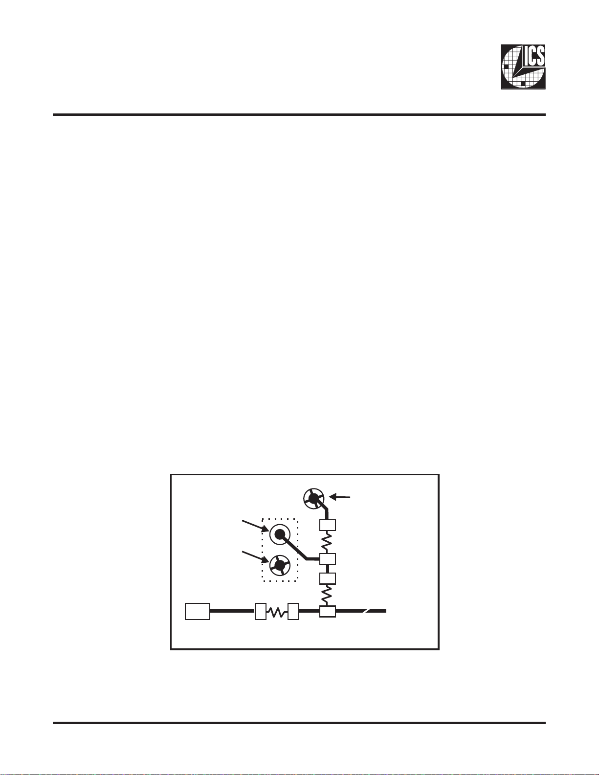
Figure 1 shows a means of implementing this function
when a switch or 2 pin header is used. With no jumper is
installed the pin will be pulled high. With the jumper in
place the pin will be pulled low. If programmability is not
necessary, than only a single resistor is necessary. The
programming resistors should be located close to the
series termination resistor to minimize the current loop
area. It is more important to locate the series termination
resistor close to the driver than the programming resistor.
0802F—04/22/05
Programming
Header
Via to Gnd
Device
Pad
Via to
VDD
2K W
8.2K W
Clock trace to load
Series Term. Res.
Fig. 1
14
Page 15
ICS950405
INDEX
AREA
1 2
h x 45°
SEATING
PLANE
- C -
.10 (.004) C
N
INDEX
AREA
12
D
e
b
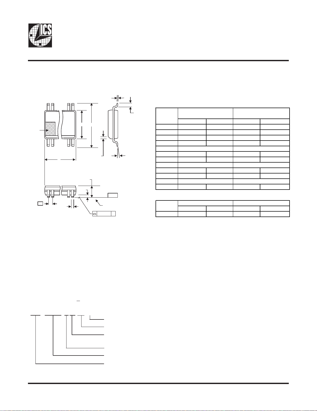
300 mil SSOP Package
c
L
E1
E
SYMBOL
A 2.41 2.80 .095 .110
In Millimeters In Inches
COMMON DIMENSIONS COMMON DIMENSIONS
MIN MAX MIN MAX
A1 0.20 0.40 .008 .016
b 0.20 0.34 .008 .0135
c 0.13 0.25 .005 .010
h x 45°
D
a
E 10.03 10.68 .395 .420
SEE VARIATIONS SEE VARIATIONS
E1 7.40 7.60 .291 .299
e
0.635 BASIC 0.025 BASIC
h 0.38 0.64 .015 .025
A
A1
-C-
SEATING
PLANE
.10 (.004) C
L 0.50 1.02 .020 .040
N
α
SEE VARIATIONS SEE VARIATIONS
0° 8° 0° 8°
VARIATIONS
N
D mm. D (inch)
MIN MAX MIN MAX
48 15.75 16.00 .620 .630
Reference Doc.: JEDEC Publication 95, MO-118
10-0034
Ordering Information
ICS950405yFLF-T
Example:
ICS XXXX y F LF- T
0802F—04/22/05
Designation for tape and reel packaging
Lead Free (Optional)
Package Type
F = SSOP
Revision Designator (will not correlate with datasheet revision)
Device Type
Prefix
ICS = Standard Device
15
Page 16
ICS950405
Revision History
Rev. Issue Date Description Page #
0.1 4/21/2005 Updated Byte 11/12 M/N programming description 8-9
0802F—04/22/05
16
 Loading...