

Page 1
Integrated
Circuit
Systems, Inc.
ICS94206
94206 Rev B 04/26/01
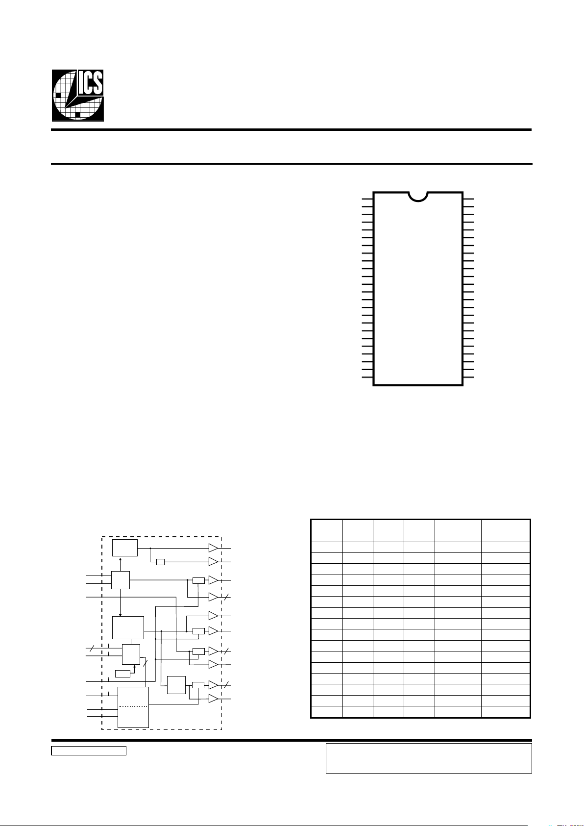
Pin Configuration
Recommended Application:
440BX - VIA Apollo Pro133 - ALI 1631 style chipset.
Output Features:
• 2 - CPUs @2.5V
• 1 - IOAPIC @ 2.5V
• 13 - SDRAM @ 3.3V
• 6 - PCI @3.3V,
• 1 - 48MHz, @3.3V
• 1 - 24MHz @ 3.3V
• 2 - REF @3.3V, 14.318MHz.
Features:
• Programmable ouput frequency.
• Programmable ouput rise/fall time.
• Programmable PCI_F and PCICLK skew.
• Spread spectrum for EMI control typically by 7dB to
8dB,
with programmable spread percentage.
• Watchdog timer technology to reset system
if over-clocking causes malfunction.
• Uses external 14.318MHz crystal.
• FS pins for frequency select
Key Specifications:
• CPU – CPU: <175ps
• SDRAM - SDRAM: <500ps
• PCI – PCI: <500ps
• CPU(early)-PCI: Min=1.0ns, Typ=2.0ns, Max=4.0ns
Programmable System Frequency Generator for PII/III™
Block Diagram
48-Pin 300mil SSOP
CLK_STOP#
PCI_STOP#
PLL2
PLL1
Spread
Spectrum
48MHz
24MHz
IOAPIC
CPUCLK_F
CPUCLK 1
SDRAM (11:0)
PCICLK (4:0)
PCICLKF
SDRAM_F
X1
X2
BUFFER IN
XTAL
OSC
PCI
CLOCK
DIVDER
STOP
STOP
STOP
STOP
S DATA
SCLK
FS(3:0)
MODE
Control
Logic
Config.
Reg.
/2
REF(1:0)
LATCH
POR
2
12
5
4
4
VDD1
*PCI_STOP/REF0
GND
X1
X2
VDD2
*MODE/PCICLK_F
**FS3/PCICLK0
GND
PCICLK1
PCICLK2
PCICLK3
PCICLK4
VDD2
BUFFER IN
GND
SDRAM11
SDRAM10
VDD3
SDRAM9
SDRAM8
GND
S DATA
SCLK
VDDL1
IOAPIC
REF1/FS2*
GND
CPUCLK_F
CPUCLK1
VDDL2
CLK_STOP#*
SDRAM_F
GND
SDRAM0
SDRAM1
VDD3
SDRAM2
SDRAM3
GND
SDRAM4
SDRAM5
VDD3
SDRAM6
SDRAM7
VDD4
48MHz/FS0*
24MHz/FS1*
ICS94206
1
2
3
4
5
6
7
8
9
10
11
12
13
14
15
16
17
18
19
20
21
22
23
24
48
47
46
45
44
43
42
41
40
39
38
37
36
35
34
33
32
31
30
29
28
27
26
25
* Internal Pull-up Resistor of 120K to VDD
** Internal Pull-down resistor of 120K to GND
Functionality
3SF2SF1SF0SF
UPC
)zHM(
KLCICP
)zHM(
0000 00.0800.04
0001 00.5705.73
0010 13.3856.14
0011 28.6614.33
0100 00.30133.43
0101 10.21143.73
0110 10.8610.43
0111 32.00114.33
1000 00.02100.04
1001 99.41133.83
1010 99.90166.63
1011 00.50100.53
1100 00.04100.53
1101 00.05105.73
1110 00.42100.13
1111 99.23152.33
ICS reserves the right to make changes in the device data identified in
this publication without further notice. ICS advises its customers to
obtain the latest version of all device data to verify that any
information being relied upon by the customer is current and accurate.
Page 2
2
ICS94206
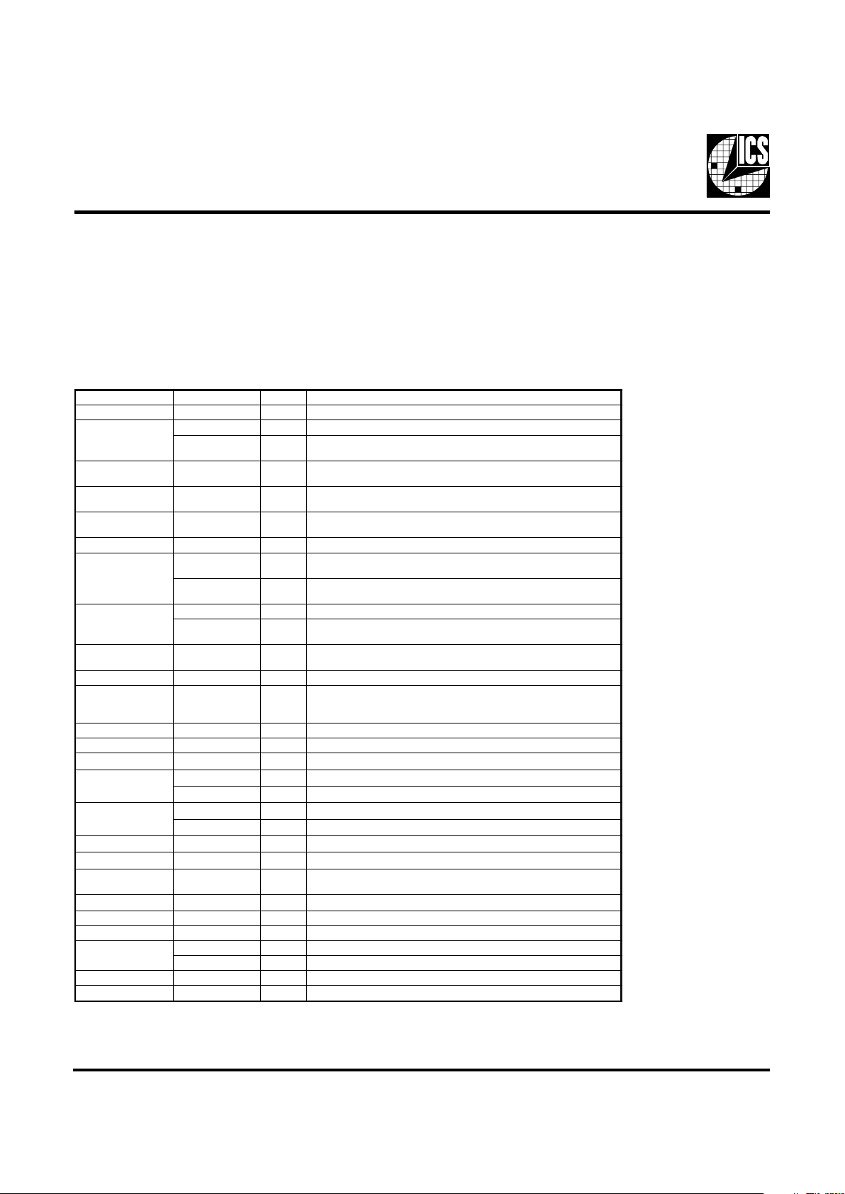
General Description
Pin Configuration
The ICS94206 is a single chip clock solution for desktop designs using the BX/Apollo Pro133/ALI 1631 style chipset. It provides all
necessary clock signals for such a system.
The ICS94206 belongs to ICS new generation of programmable system clock generators. It employs serial programming I
2
C
interface as a vehicle for changing output functions, changing output frequency, configuring output strength, configuring output to
output skew, changing spread spectrum amount, changing group divider ratio and dis/enabling individual clocks. This device also
has ICS propriety 'Watchdog Timer' technology which will reset the frequency to a safe setting if the system become unstable from
over clocking.
Notes:
1: Internal Pull-up Resistor of 120K to 3.3V on indicated inputs
2: Bidirectional input/output pins, input logic levels are latched at internal power-on-reset. Use 10Kohm resistor
to program logic Hi to VDD or GND for logic low.
REBMUNNIPEMANNIPEPYTNOITPIRCSED
11DDVRWPV3.3lanimon,ylppusrewopLATX,feR
2
0FERTUO.kcolcecnereferzhM813.41
#POTS_ICP
1
NI
elibomnI(woltupninehw,level0cigoltaskcolcKLCICPstlaH
)0=EDOM,edom
,22,61,9,3
54,93,33
DNGRWPdnuorG
41XNI
kcabdeefdna)Fp63(pacdaollanretnisah,tupnilatsyrC
2Xmorfrotsiser
52XTUO
daollanretnisaH.zHM813.41yllanimon,tuptuolatsyrC
)Fp63(pac
41,62DDVRWPV3.3lanimon,)4:0(KLCICPdnaF_KLCICProfylppuS
7
F_KLCICPTUO
rewoprof#POTS_ICPybdetceffatonkcolcICPgninnureerF
.tnemeganam
EDOM
2,1
NI
.edoMeliboM=0,edoMpotkseD=1,niptcelesnoitcnuf7niP
.tupnIdehctaL
8
3SFNIDNGotnwod-lluPlanretnI.tupnIdehctaL.niptcelesycneuqerF
0KLCICPTUO
wekssn84-1htiwskcolcUPCotsuonorehcnyS.stuptuokcolcICP
)ylraeUPC(
01,11,21,31)1:4(KLCICPTUO
wekssn84-1htiwskcolcUPCotsuonorehcnyS.stuptuokcolcICP
)ylraeUPC(
51NIREFFUBNI.stuptuoMARDSrofsreffuBtuonaFottupnI
,12,02,81,71
,23,13,92,82
83,73,53,43
)0:11(MARDSTUO
nipNIREFFUBmorfstuptuoreffuBtuonaF,stuptuokcolcMARDS
.)tespihcybdellortnoc(
63,03,913DDVRWP.V3.3lanimon,eroCLLPUPCdna)21:0(MARDSrofylppuS
32ATADSO/IIrofnipataD
2
tnarelotV5yrtiucricC
42KLCSNIIfotupnikcolC
2
tupnitnarelotV5,tupniC
52
zHM42TUOkcolctuptuozHM42
1SF
2,1
NI.tupnIdehctaL.niptcelesycneuqerF
62
zHM84TUOkcolctuptuozHM84
0SF
2,1
NItupnIdehctaL.niptcelesycneuqerF
724DDVRWP.erocLLPdexifdnasreffubtuptuozHM84&42rofrewoP
04F_MARDSTUO#POTS_UPCybdetceffatoN.tuptuokcolcMARDSgninnureerF
14#POTS_KLCNI
MARDS&CIPAOI,1KLCUPCstlahtupnisuonorhcnysasihT
.wolnevirdnehwlevel"0"cigolta)11:0(
242LDDVRWPlanimonV3.3roV5.2rehtie,skcolcUPCrofylppuS
341KLCUPCTUOwoL=#POTS_UPCfiwoL.2LDDVybderewop,stuptuokcolcUPC
44F_KLCUPCTUO#POTS_UPCehtybdetceffatoN.kcolcUPCgninnureerF
64
1FERTUO.kcolcecnereferzHM813.41
2SF
2,1
NItupnIdehctaL.niptcelesycneuqerF
74CIPAOITUOCIPAOI.1LDDVybderewoPzHM813.41.tuptuokcolc
841LDDVRWPlanimonV3.3ro5.2rehtie,CIPAOIrofylppuS
Page 3
3
ICS94206
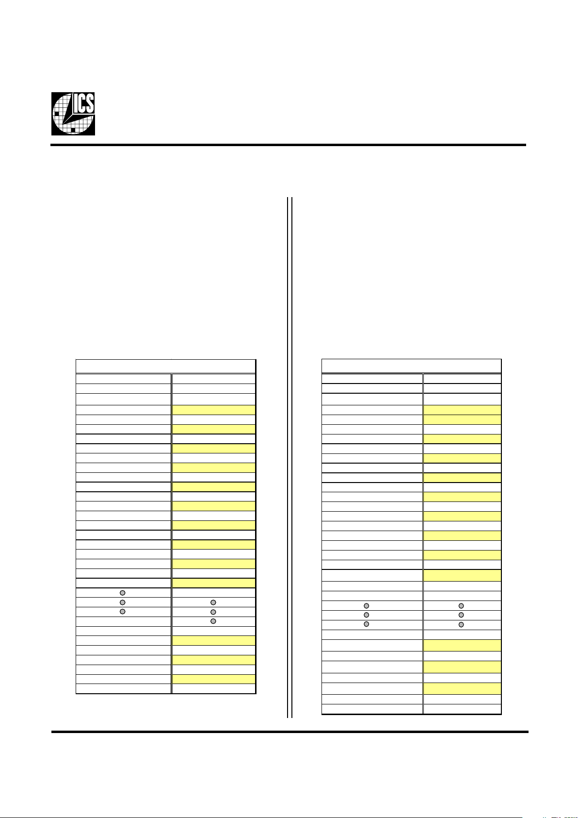
General I2C serial interface information for the ICS94206
How to Write:
• Controller (host) sends a start bit.
• Controller (host) sends the write address D2
(H)
• ICS clock will acknowledge
• Controller (host) sends a dummy command code
• ICS clock will acknowledge
• Controller (host) sends a dummy byte count
• ICS clock will acknowledge
• Controller (host) starts sending Byte 0 through Byte 20
(see Note)
• ICS clock will acknowledge each byte one at a time
• Controller (host) sends a Stop bit
How to Read:
• Controller (host) will send start bit.
• Controller (host) sends the read address D3
(H)
• ICS clock will acknowledge
• ICS clock will send the byte count
• Controller (host) acknowledges
• ICS clock sends Byte 0 through byte 8 (default)
• ICS clock sends Byte 0 through byte X (if X
(H)
was
written to byte 8).
• Controller (host) will need to acknowledge each byte
• Controller (host) will send a stop bit
Controll e r (Host)
ICS (Slave/Receiver)
Start Bit
Address D2
(H)
ACK
Dumm y Comm an d Code
ACK
Dumm y B y te Count
ACK
Byte 0
ACK
Byte 1
ACK
Byte 2
ACK
Byte 3
ACK
Byte 4
ACK
Byte 5
ACK
Byte 6
ACK
Byte 18
ACK
Byte 19
ACK
Byte 20
ACK
Stop Bit
How to Write:
*See notes on the following page.
Controlle r (Host)
ICS (Slave/Receiver)
Start Bit
Address D3
(H)
ACK
Byte Count
ACK
Byte 0
ACK
Byte 1
ACK
Byte 2
ACK
Byte 3
ACK
Byte 4
ACK
Byte 5
ACK
Byte 6
ACK
If 7
H
has been written to B 6
Byte 7
ACK
If 12
H
has been written to B 6
Byte18
ACK
If 13
H
has been written to B 6
Byte 19
ACK
If 14
H
has been written to B 6
Byte 20
ACK
Stop Bit
How to Read:
Page 4
4
ICS94206
1. The ICS clock generator is a slave/receiver, I2C component. It can read back the data stored in the latches for verification.
Readback will support standard SMBUS controller protocol. The number of bytes to readback is defined by writing to
byte 8.
2. When writing to byte 11 - 12, and byte 13 - 14, they must be written as a set. If for example, only byte 14 is written
but not 15, neither byte 14 or 15 will load into the receiver.
3. The data transfer rate supported by this clock generator is 100K bits/sec or less (standard mode)
4. The input is operating at 3.3V logic levels.
5. The data byte format is 8 bit bytes.
6. To simplify the clock generator I
2
C interface, the protocol is set to use only Block-Writes from the controller. The bytes
must be accessed in sequential order from lowest to highest byte with the ability to stop after any complete byte has been
transferred. The Command code and Byte count shown above must be sent, but the data is ignored for those two bytes.
The data is loaded until a Stop sequence is issued.
7. At power-on, all registers are set to a default condition, as shown.
Notes:
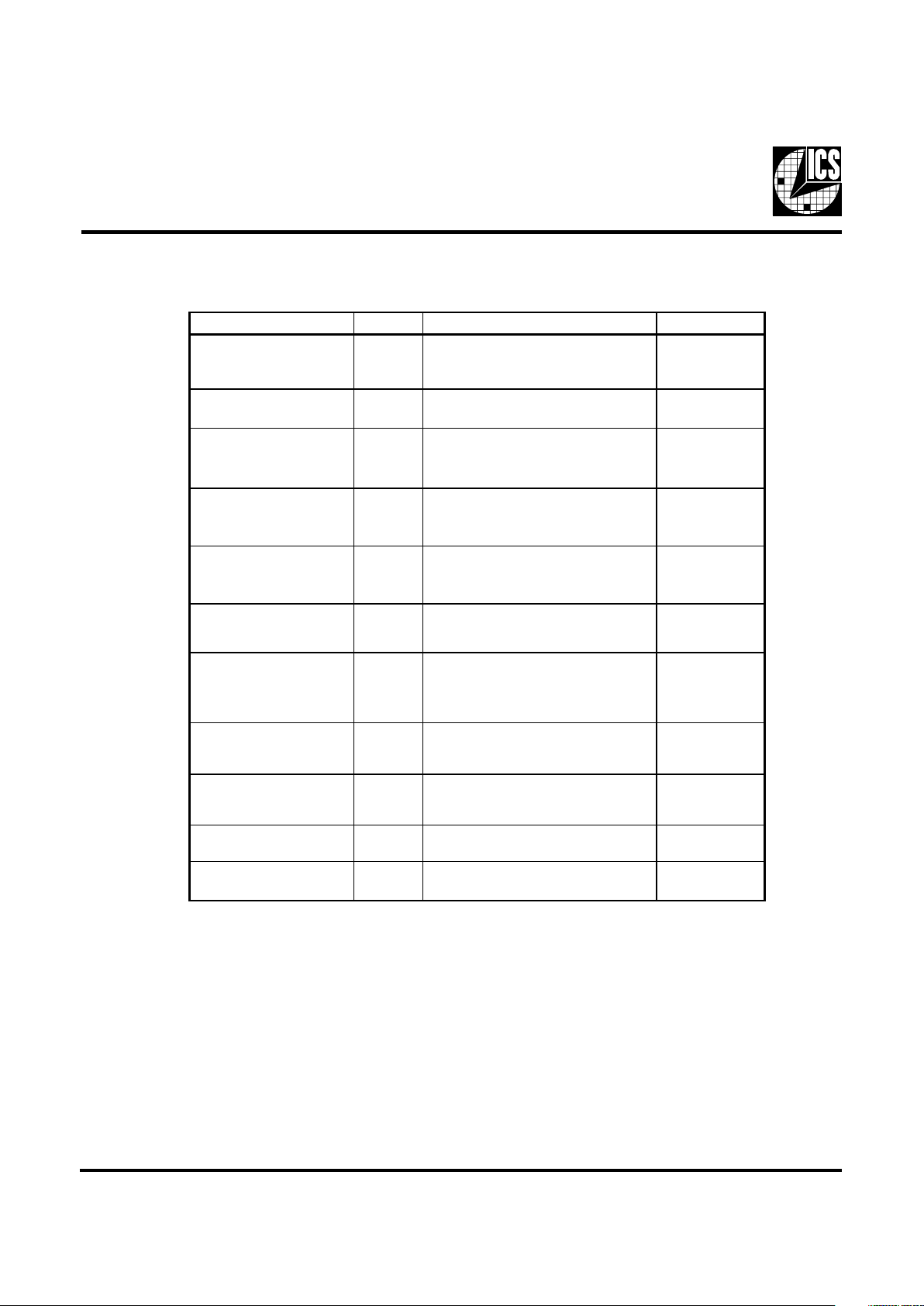
Brief I2C registers description for ICS94206
Programmable System Frequency Generator
Register N ame Byte Description PWD D efau lt
Functionality & Frequency
Select Register
0
Output frequency, hardware / I
2
C
frequ ency s elect, spread spectrum &
output enable control register.
See individual
byte description
Output Con trol R egis ters 1-6
Active / inactive outpu t control
registers/latch inputs read back.
See individual
byte description
Vendor ID & Revision ID
Registers
7
Byte 11 bit[7:4] is ICS vendor id - 1001.
Other bits in this register designate device
revision ID of this part.
See individual
byte description
Byte Cou nt
Read Back Register
8
Writing to this regis ter w ill con figure
byte count and how many byte will be
read back. Do not write 00
H
to this by te.
08
H
Watchdog Timer
Count Register
9
Writing to this regis ter w ill con figure the
number of seconds for the watchdog
timer to res et.
10
H
Watchdog Control Registers 10 Bit [6:0]
Watchdog enable, watchdog status and
programmable 'safe' frequency' can be
confi
g
ured in th is register .
000,0000
VCO Control Selectio n Bit 10 Bit [7]
This bit s elect w heth er the outp ut
frequency is control by hardware/byte 0
configurations or byte 11&12
programming.
0
VCO Frequency Control
Registers
11-12
These registers control the dividers ratio
into the phase detector and thus control
the V CO output frequency.
Depended on
hardware/byte 0
configuration
Spread Spectrum Control
Registers
13-14
Thes e registers control the spread
percentage amount.
Depended on
hardware/byte 0
configuration
Group Skews Control
Registers
15-16
Increment or decrement the group skew
amount as com pared to th e initial s kew .
See individual
byte description
Output Rise/Fall Time
Select Registers
17-20
Thes e registers w ill control the output
rise and fall time.
See individual
byte description
Page 5
5
ICS94206
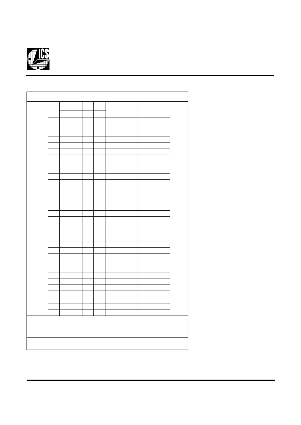
Byte 0: Functionality and frequency select register (Default=0)
Notes:
1.
Default at power-up will be for latched logic inputs to define frequency, as displayed by Bit 3.
tiB
noitpircseD
DWP
tiB
)4:7,2(
2tiB
7tiB6tiB5tiB4tiB
zHMKLCUPC
KLCICP
zHM
1etoN
3SF2SF1SF0SF
00000 00.0800.04
00001 00.5705.73
00010 13.3856.14
00011 28.6614.33
00100 00.30133.43
00101 10.21143.73
00110 10.8610.43
00111 32.00114.33
01000 00.02100.04
01001 99.41133.83
01010 99.90166.63
01011 00.50100.53
01100 00.04100.53
01101 00.05105.73
01110 00.42100.13
01111 99.23152.33
10000 00.53157.33
10001 99.92105.23
10010 00.62105.13
10011 00.81133.93
10100 89.51166.83
10101 00.5976.13
10110 00.0900.03
10111 10.5843.82
11000 00.66105.14
11001 10.06100.04
11010 99.45157.83
11011 59.74199.63
11100 89.54105.63
11101 89.34199.53
11110 99.14105.53
11111 10.83105.43
3tiB
stupnidehctal,tceleserawdrahybdetcelessiycneuqerF-0
4:7,2tiBybdetcelessiycneuqerF-1
0
1tiB
lamroN-0
daerpSretneC%53.0±elbanemurtcepsdaerpS-1
1
0tiB
gninnuR-0
stuptuollaetatsirT-1
0
Page 6
6
ICS94206
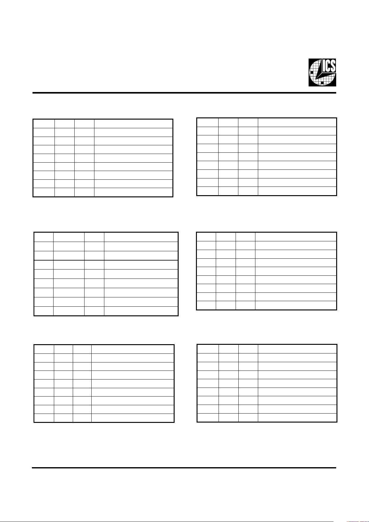
Byte 1: CPU, Active/Inactive Register
(1= enable, 0 = disable)
Byte 2: PCI, Active/Inactive Register
(1= enable, 0 = disable)
TIB#NIPDWPNOITPIRCSED
7tiB-1 )devreseR(
6tiB71 F_KLCICP
5tiB-1 )devreseR(
4tiB311 4KLCICP
3tiB211 3KLCICP
2tiB111 2KLCICP
1tiB011 1KLCICP
0tiB81 0KLCICP
Notes:
1. Inactive means outputs are held LOW and are disabled
from switching.
2. Latched Frequency Selects (FS#) will be inverted logic
load of the input frequency select pin conditions.
TIB#NIPDWPNOITPIRCSED
7tiB-1 )devreseR(
6tiB-1 )devreseR(
5tiB-1 )devreseR(
4tiB-1 )devreseR(
3tiB-X #1SFdehctaL
2tiB-1 )devreseR(
1tiB-X #3SFdehctaL
0tiB-1 )devreseR(
Byte 4: Reserved , Active/Inactive Register
(1= enable, 0 = disable)
TIB#NIPDWPNOITPIRCSED
7tiB-1 )devreseR(
6tiB-1 )devreseR(
5tiB-1 )devreseR(
4tiB741 0CIPAOI
3tiB-1 )devreseR(
2tiB-1 )devreseR(
1tiB641 1FER
0tiB210FER
Byte 5: Peripheral , Active/Inactive Register
(1= enable, 0 = disable)
Byte 3: SDRAM, Active/Inactive Register
(1= enable, 0 = disable)
TIB#NIPDWPNOITPIRCSED
7tiB-1 )devreseR(
6tiB-X #0SFdehctaL
5tiB621zHM84
4tiB521 zHM42
3tiB-1 )devreseR(
2tiB71,81,02,121 )11:8(MARDS
1tiB82,92,13,231 )7:4(MARDS
0tiB43,53,73,831 )3:0(MARDS
TIB#NIPDWPNOITPIRCSED
7tiB-0 )etoN(devreseR
6tiB-0 )etoN(devreseR
5tiB-0 )etoN(devreseR
4tiB-0 )etoN(devreseR
3tiB-0 )etoN(devreseR
2tiB-1 )etoN(devreseR
1tiB-1 )etoN(devreseR
0tiB-0 )etoN(devreseR
Byte 6: Peripheral , Active/Inactive Register
(1= enable, 0 = disable)
Note: This is an unused register writing to this register will not
affect device performance or functinality.
TIB#NIPDWPNOITPIRCSED
7tiB-X #2SFdehctaL
6tiB-1 )devreseR(
5tiB-1 )devreseR(
4tiB-1 )devreseR(
3tiB041 F_MARDS
2tiB-1 )devreseR(
1tiB341 1KLCUPC
0tiB441 F_KLCUPC
Page 7
7
ICS94206
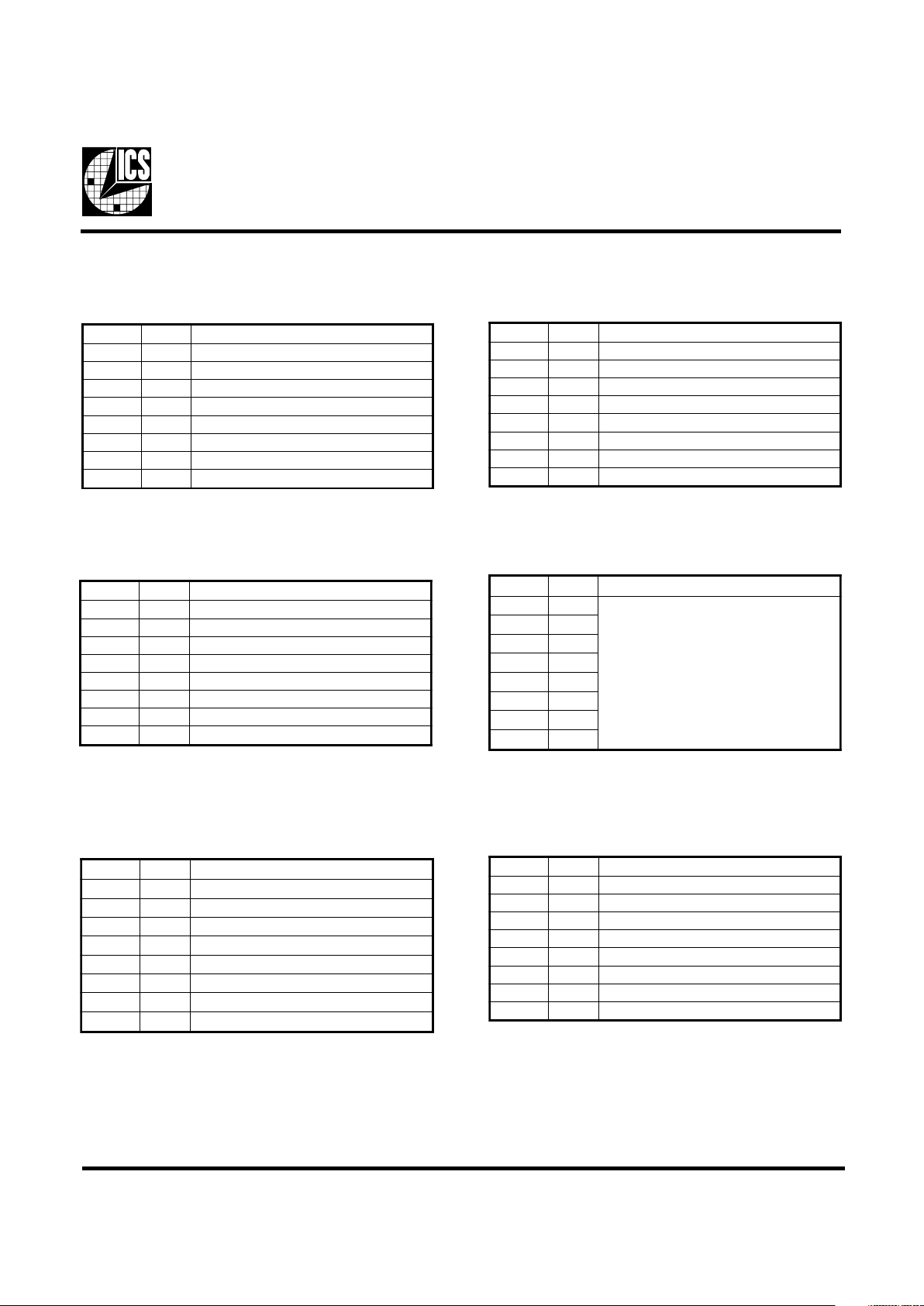
Byte 7: Vendor ID and Revision ID Register
Byte 8: Byte Count and Read Back Register
Notes:
1. PWD = Power on Default
tiBDWPnoitpircseD
7tiB0 devreseR
6tiB0 devreseR
5tiB0 devreseR
4tiB0 devreseR
3tiB1 devreseR
2tiB0 devreseR
1tiB0 devreseR
0tiB0 devreseR
tiBDWPnoitpircseD
7tiB0 DIrodneV
6tiB0 DIrodneV
5tiB1 DIrodneV
4tiBX DInoisiveR
3tiBX DInoisiveR
2tiBX DInoisiveR
1tiBX DInoisiveR
0tiBX DInoisiveR
Byte 11: VCO Frequency Control Register
Note: The decimal representation of these 7 bits (Byte 11
[6:0]) + 2 is equal to the REF divider value .
tiBDWPnoitpircseD
7tiBX 0tiBrediviDOCV
6tiBX 6tiBrediviDFER
5tiBX 5tiBrediviDFER
4tiBX 4tiBrediviDFER
3tiBX 3tiBrediviDFER
2tiBX 2tiBrediviDFER
1tiBX 1tiBrediviDFER
0tiBX 0tiBrediviDFER
Byte 12: VCO Frequency Control Register
Note: The decimal representation of these 9 bits (Byte 12 bit
[7:0] & Byte 11 bit [7] ) + 8 is equal to the VCO divider value.
For example if VCO divider value of 36 is desired, user need
to program 36 - 8 = 28, namely, 0, 00011100 into byte 12 bit
& byte 11 bit 7.
tiBDWPnoitpircseD
7tiBX 8tiBrediviDOCV
6tiBX 7tiBrediviDOCV
5tiBX 6tiBrediviDOCV
4tiBX 5tiBrediviDOCV
3tiBX 4tiBrediviDOCV
2tiBX 3tiBrediviDOCV
1tiBX 2tiBrediviDOCV
0tiBX 1tiBrediviDOCV
Byte 10: Watchdog Timer Count Register
tiBDWPnoitpircseD
7tiB0
esehtfonoitatneserperlamicedehT
sm1rosm092otdnopserrocstib8
erofebtiawlliwremitgodhctaweht
ehtteserdnaedommralaotseogti
tluafeD.gnittesefasehtotycneuqerf
6.4=sm092X61sipurewopta
.sdnoces
6tiB0
5tiB0
4tiB1
3tiB0
2tiB0
1tiB0
0tiB0
Note: FS values in bit [0:4] will correspond to Byte 0 FS
values. Default safe frequency is same as 00000 entry in
byte0.
Byte 9: VCO Control Selection Bit &
Watchdog Timer Control Register
tiBDWPnoitpircseD
7tiB0 qerf51&41B=1/qerf0B/wH=0
6tiB0 elbane=1/elbasid=0elbanEDW
5tiB0 mrala=1/lamron=0sutatSDW
4tiB0 2tib0etyB,ycneuqerFefaSDW
3tiB0 3SF,ycneuqerFefaSDW
2tiB0 2SF,ycneuqerFefaSDW
1tiB0 1SF,ycneuqerFefaSDW
0tiB0 0SF,ycneuqerFefaSDW
Page 8
8
ICS94206
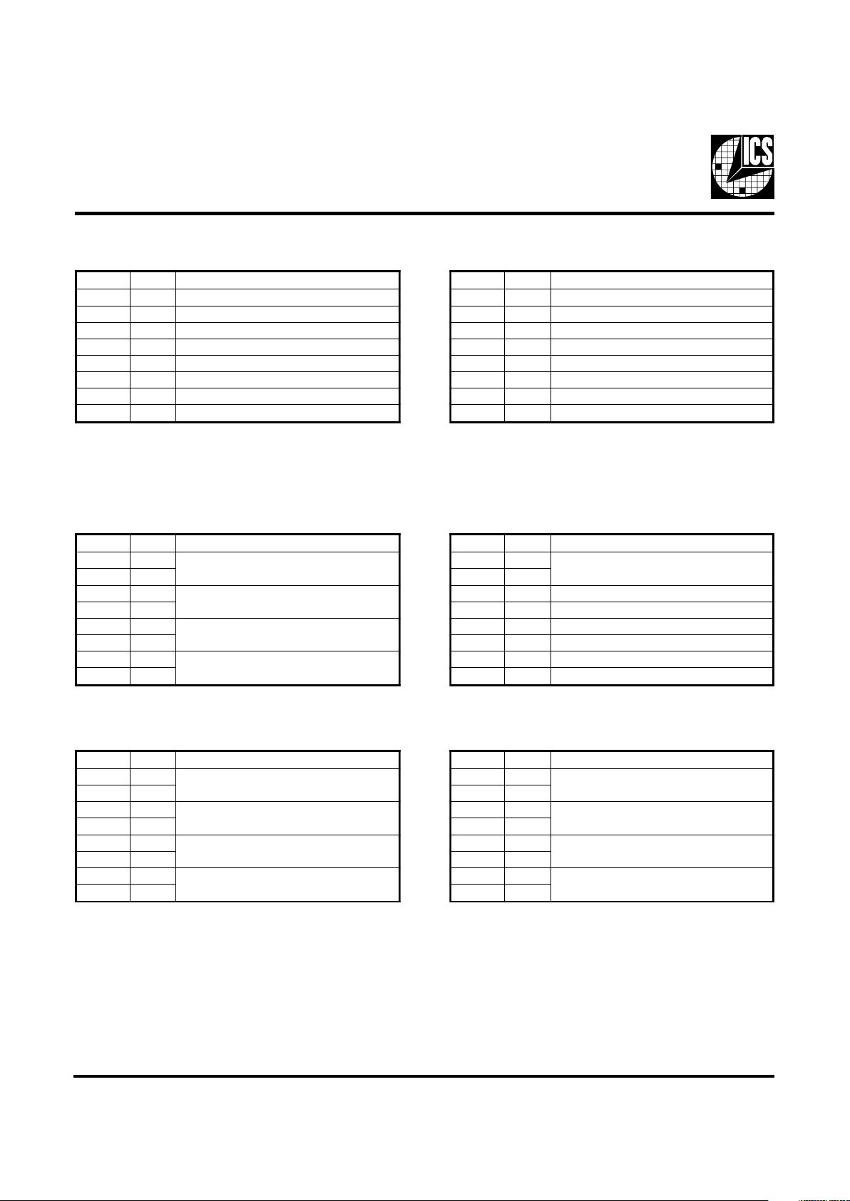
Byte 13: Spread Sectrum Control Register Byte 14: Spread Sectrum Control Register
Note: Please utilize software utility provided by ICS
Application Engineering to configure spread spectrum.
Incorrect spread percentage may cause system failure.
tiBDWPnoitpircseD
7tiBX 7tiBmurtcepSdaerpS
6tiBX 6tiBmurtcepSdaerpS
5tiBX 5tiBmurtcepSdaerpS
4tiBX 4tiBmurtcepSdaerpS
3tiBX 3tiBmurtcepSdaerpS
2tiBX 2tiBmurtcepSdaerpS
1tiBX 1tiBmurtcepSdaerpS
0tiBX 0tiBmurtcepSdaerpS
tiBDWPnoitpircseD
7tiBX devreseR
6tiBX devreseR
5tiBX devreseR
4tiBX 21tiBmurtcepSdaerpS
3tiBX 11tiBmurtcepSdaerpS
2tiBX 01tiBmurtcepSdaerpS
1tiBX 9iBmurtcepSdaerpS
0tiBX 8tiBmurtcepSdaerpS
Note: Please utilize software utility provided by ICS
Application Engineering to configure spread spectrum.
Incorrect spread percentage may cause system failure.
Byte 15: Output Skew Control Byte 16: Output Skew Control
tiBDWPnoitpircseD
7tiB
lortnoCwekSF_ICP
6tiB
5tiB
lortnoCwekS}4:0[KLCICP
4tiB
3tiB
lortnoCwekSF_MARDS
2tiB
1tiB
lortnoCwekS}7:0[MARDS
0tiB
tiBDWPnoitpircseD
7tiB
lortnoCwekS]11:8[MARDS
6tiB
5tiBX devreseR
4tiBX devreseR
3tiBX devreseR
2tiBX devreseR
1tiBX devreseR
0tiBX devreseR
Byte 17: Output Rise/Fall Time Select Register Byte 18: Output Rise/Fall Time Select Register
tiBDWPnoitpircseD
7tiB
lortnoCetaRwelS:F_KLCUPC
6tiB
5tiB
lortnoCetaRwelS:1KLCUPC
4tiB
3tiB
lortnoCetaRwelS:F_MARDS
2tiB
1tiB
lortnoCetaRwelS]11:0[MARDS
0tiB
tiBDWPnoitpircseD
7tiB
lortnoCetaRwelS:]4:0{ICP
6tiB
5tiB
lortnoCetaRwelSF_ICP
4tiB
3tiB
lortnoCetaRwelS:zHM84
2tiB
1tiB
lortnoCetaRwelS:zHM42
0tiB
Notes:
1. PWD = Power on Default
2. The power on default for byte 13-20 depends on the harware (latch inputs FS[0:4]) or I
2
C (Byte 0 bit [1:7]) setting. Be sure to read
back and re-write the values of these 8 registers when VCO frequency change is desired for the first pass.
3. If Byte 8 bit 7 is driven to "1" meaning programming is intended, Byte 21-24 will lose their default power up value.
Page 9
9
ICS94206
VCO Programming Constrains
VCO Frequency ...................... 150MHz to 500MHz
VCO Divider Range ................ 8 to 519
REF Divider Range ................. 2 to 129
Phase Detector Stability .......... 0.3536 to 1.4142
Useful Formula
VCO Frequency = 14.31818 x VCO/REF divider value
Phase Detector Stabiliy = 14.038 x (VCO divider value)
-0.5
Note:
1. User needs to ensure step 3 & 7 is carried out. Systems with wrong spread percentage and/or group to group skew relation
programmed into bytes 13-16 could be unstable. Step 3 & 7 assure the correct spread and skew relationship.
2. If VCO, REF divider values or phase detector stability are out of range, the device may fail to function correctly.
3. Follow min and max VCO frequency range provided. Internal PLL could be unstable if VCO frequency is too fast or too slow.
Use 14.31818MHz x VCO/REF divider values to calculate the VCO frequency (MHz).
4. ICS recommends users, to utilize the software utility provided by ICS Application Engineering to program the VCO
frequency.
5. Spread percent needs to be calculated based on VCO frequency, spread modulation frequency and spreadamount desired. See
Application note for software support.
To program the VCO frequency for over-clocking.
0. Before trying to program our clock manually, consider using ICS provided software utilities for easy programming.
1. Select the frequency you want to over-clock from with the desire gear ratio (i.e. CPU:SDRAM:3V66:PCI ratio) by
writing to byte 0, or using initial hardware power up frequency.
2. Write 0001, 1001 (19H) to byte 8 for readback of 21 bytes (byte 0-20).
3. Read back byte 11-20 and copy values in these registers.
4. Re-initialize the write sequence.
5. Write a '1' to byte 9 bit 7 and write to byte 11 & 12 with the desired VCO & REF divider values.
6. Write to byte 13 to 20 with the values you copy from step 3. This maintains the output spread, skew and slew rate.
7. The above procedure is only needed when changing the VCO for the 1st pass. If VCO frequency needed to be changed
again, user only needs to write to byte 11 and 12 unless the system is to reboot.
tiBDWPnoitpircseD
7tiBX devreseR
6tiBX devreseR
5tiBX devreseR
4tiBX devreseR
3tiBX devreseR
2tiBX devreseR
1tiBX devreseR
0tiBX devreseR
Byte 19: Reserved Register
Note: Byte 19 and 20 are reserved registers, these are
unused registers writing to these registers will not
affect device performance or functinality.
tiBDWPnoitpircseD
7tiBX devreseR
6tiBX devreseR
5tiBX devreseR
4tiBX devreseR
3tiBX devreseR
2tiBX devreseR
1tiBX devreseR
0tiBX devreseR
Byte 20: Reserved Register
Page 10
10
ICS94206
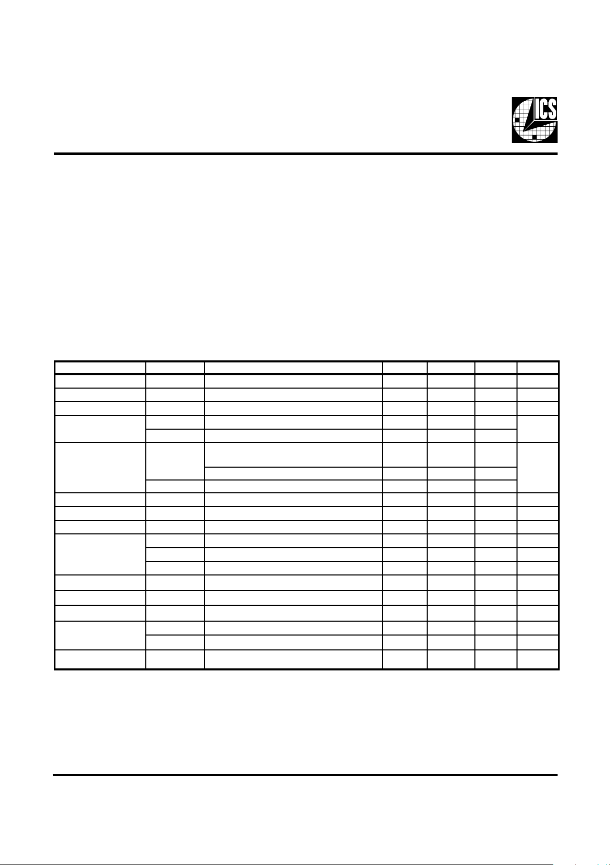
Absolute Maximum Ratings
Supply Voltage . . . . . . . . . . . . . . . . . . . . . . . . . . . . 7.0 V
Logic Inputs . . . . . . . . . . . . . . . . . . . . . . . . . . . . . . . GND –0.5 V to V
DD
+0.5 V
Ambient Operating Temperature . . . . . . . . . . . . . . 0°C to +70°C
Case Temperature . . . . . . . . . . . . . . . . . . . . . . . . . . 115°C
Storage Temperature . . . . . . . . . . . . . . . . . . . . . . . . –65°C to +150°C
Stresses above those listed under Absolute Maximum Ratings may cause permanent damage to the device. These ratings are stress
specifications only and functional operation of the device at these or any other conditions above those listed in the operational sections
of the specifications is not implied. Exposure to absolute maximum rating conditions for extended periods may affect product
reliability.
Electrical Characteristics - Input/Supply/Common Output Parameters
TA = 0 - 70C; Supply Voltage VDD = 3.3 V +/-5%, V
DDL
= 2.5 V +/-5% (unless otherwise stated)
PARAMETER SYMBOL CONDITIONS MIN TYP MAX UNITS
Input High Voltage V
IH
2V
DD
+0.3 V
Input Low Voltage V
IL
VSS-0.3 0.8 V
Input High Current I
IH
VIN = V
DD
-5 5
µ
A
I
IL1
VIN = 0 V; Inputs with no pull-up resistors -5
I
IL2
VIN = 0 V; Inputs with pull-up resistors -200
C
L
= max cap loads;
CPU=66-133 MHz
,
SDRAM=100 MHz
124 350
CPU=133 MHz, SDRAM=133 MHz 135 500
I
DD2.5OP
CL = max cap loads;
18 70
Powerdown Current
I
DD3.3PD
CL = 0 pF; Input address to VDD or GND
600
µ
A
Input Frequency F
i
VDD = 3.3 V 14.318 MHz
Pin Inductance L
pin
7nH
C
IN
Logic Inputs 5 pF
C
OUT
Output pin capacitance 6 pF
C
INX
X1 & X2 pins 27 45 pF
Transition time
1
T
trans
To 1st crossing of target frequency 3 ms
Settling time
1
T
s
From 1st crossing to 1% target frequency 3 ms
Clk Stabilization
1
T
STAB
From VDD = 3.3 V to 1% target frequency 3 ms
t
PZH,tPZL
Output enable delay (all outputs) 1 10 ns
t
PHZ,tPLZ
Output disable delay (all outputs) 1 10 ns
Skew
1
tcpu-pci
V
T
= 1.5V; VTL=1.25V
2.45 4 ns
1
Guaranteed by design, not 100% tested in production.
Delay
1
Input Capacitance
1
Input Low Current
µ
A
I
DD3.3OP
Operating Supply
Current
mA
Page 11
11
ICS94206
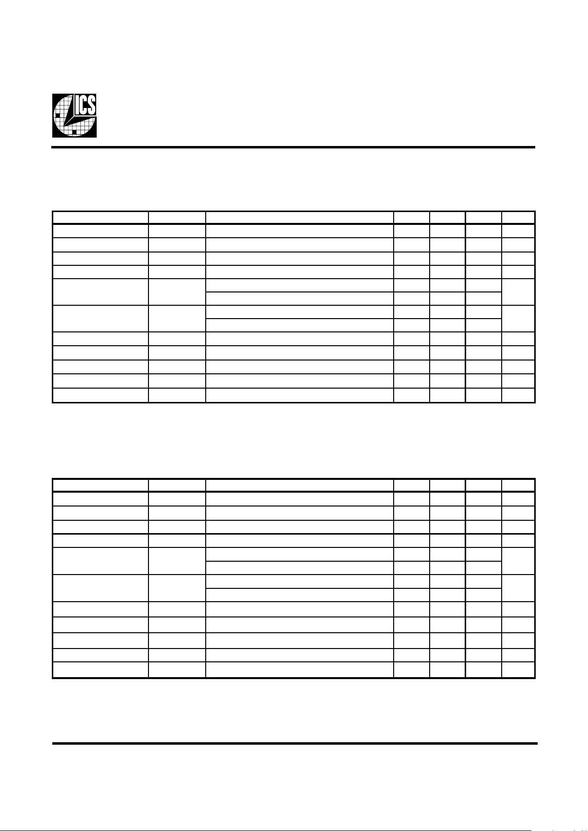
Electrical Characteristics - CPU
TA = 0 - 70º C;VDD = 3.3V; V
DDL
= 2.5 V +/-5%; CL = 10 - 20 pF (unless otherwise stated)
PARAMETER SYMBOL CONDITIONS MIN TYP MAX UNITS
Output Impedance
1
R
DSP2B
Vo=VDD*(0.5) 13.5 15 45
Ω
Output Impedance
1
R
DSN2B
Vo=VDD*(0.5) 13.5 16.5 45
Ω
Output High Voltage V
OH2B
IOH = -1 mA 2 2.48 V
Output Low Voltage V
OL2B
IOL = 1 mA 0.04 0.4 V
V
OH@MIN
= 1 V -60 -27
V
OH@MAX
= 2.375V -27 -7
V
OL@MIN
= 1.2 V 27 63
V
OL@MAX
=0.3V 20 30
Rise Time
1
t
r2B
VOL = 0.4 V, VOH = 2.0 V 0.4 1.2 1.6 ns
Fall Time
1
t
f2B
VOH = 2.0 V, VOL = 0.4 V 0.4 0.9 1.6 ns
Duty Cycle
1
d
t2B
VT = 1.25 V 45 46.9 55 %
Skew
1
t
sk2B
VT = 1.25 V 12.7 175 ps
Jitter, Cycle-to-cycle
1
t
jcyc-cyc2B
VT = 1.25 V, CPU 66, SDRAM 100
150 250 ps
1
Guaranteed by design, not 100% tested in production.
mA
mA
Output High Current
I
OH2B
Output Low Current
I
OL2B
Electrical Characteristics - PCI
TA = 0 - 70º C; VDD = 3.3 V +/-5%, CL = 40 pF for PCI0-1, CL = 10 - 30 pF for other PCIs (unless otherwise stated)
PARAMETER SYMBOL CONDITIONS MIN TYP MAX UNITS
Output Impedance
1
R
DSP1
Vo=V
DD
*(0.5) 12 55
Ω
Output Impedance
1
R
DSN1
Vo=V
DD
*(0.5) 12 55 Ω
Output High Voltage V
OH1
IOH = -1 mA 2.4 V
Output Low Voltage V
OL1
IOL = 1 mA 0.55 V
V
OH@MIN
= 1 V -33
V
OH@MAX
= 3.135V -33
V
OL@MIN
= 1.95 V 30
V
OL@MAX
=0.4V 38
Rise Time
1
t
r1
V
O
L
= 0.4 V, VOH = 2.4 V,
0.5
1.5 2
ns
Fall Time
1
t
f1
V
O
L
= 2.4 V, VOH = 0.4 V, PCI0-3
0.5
1.5 2
ns
Duty Cycle
1
d
t1
VT = 1.5 V 45 52.5 55 %
Skew
1
t
sk1
VT = 1.5 V 49 500
ps
Jitter, cycle-to-cycle
1
t
jcyc-cyc1
VT = 1.5 V
200 500
ps
1
Guaranteed by design, not 100% tested in production.
mA
mA
Output Hi g h Current
I
OH1
Output Low Current
I
OL1
Page 12
12
ICS94206
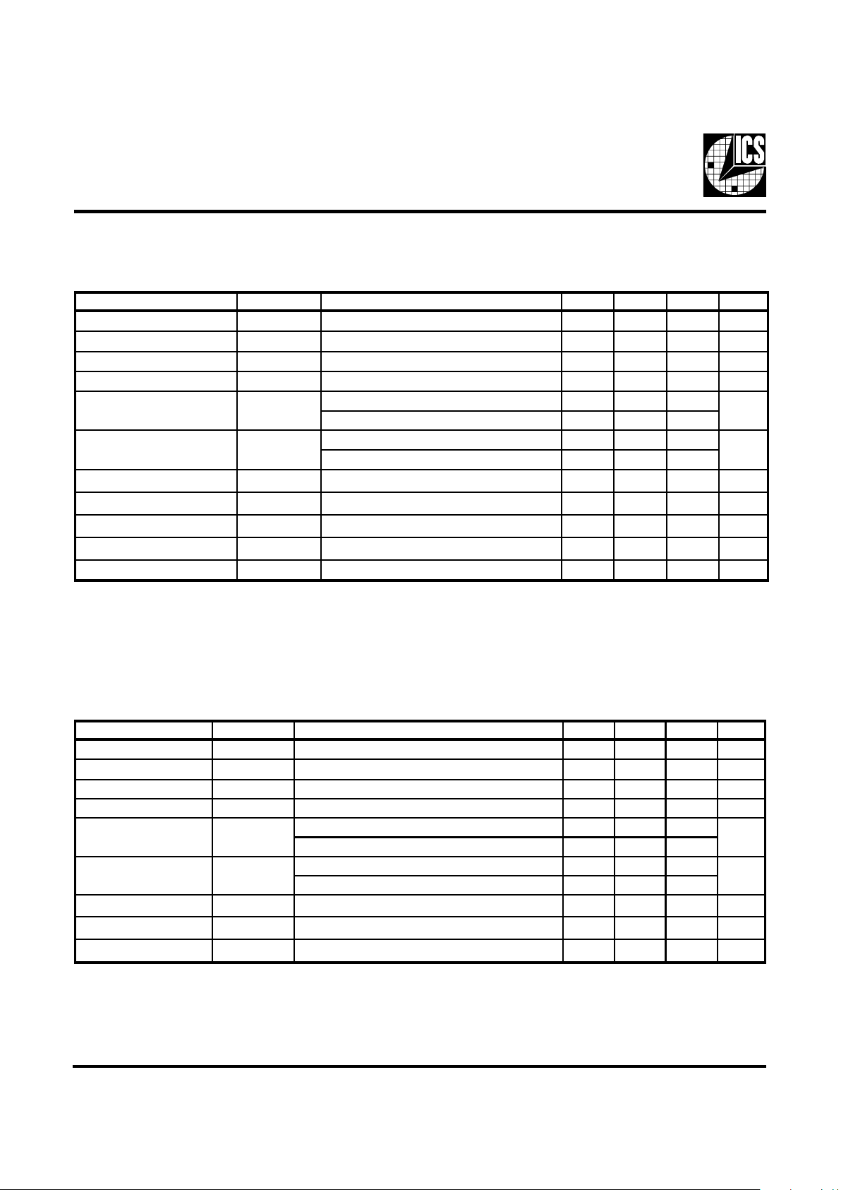
Electrical Char acteristics - SDRAM
TA = 0 - 70º C; VDD = 3.3 V +/-5%, CL = 20 - 30 pF (unless otherwise stated)
PARAMETER SYMBOL CONDITIONS MIN TYP MAX UNITS
Output Impedance
1
R
DSP3
Vo=V
DD
*(0.5) 10 24
Ω
Output Impedance
1
R
DSN3
Vo=V
DD
*(0.5) 10 24
Ω
Output High Voltage V
OH3
IOH = -1 mA 2.4 V
Output Low Voltage V
OL3
IOL = 1 mA 0.4 V
V
OH@MIN
= 2 V -46
V
OH@MAX
= 3.135V -54
V
OL@MIN
= 1 V 54
V
OL@MAX
=0.4V 53
Rise Time
1
t
r3
VOL = 0.4 V, VOH = 2.4 V 0.4 0.8 1.6 ns
Fall Time
1
t
f3
VOH = 2.4 V, VOL = 0.4 V 0.4 0.8 1.6 ns
Duty Cycle
1
d
t3
VT = 1.5 V 45 51.7 55 %
Skew
1
t
sk3
VT = 1.5 V 166 250 ps
Propagation Delay Tprop
V
T
= 1.5 V
3.1 5 ns
1
Guaranteed by design, not 100% tested in production.
mA
mA
Output High Current
I
OH3
Output Low Current
I
OL3
Electrical Characteristics - IOAPIC
TA = 0 - 70º C; VDD = 3.3V; V
DDL
= 2.5 V +/-5%; CL = 10 - 20 pF (unless otherwise stated)
PARAMETER SYMBOL CONDITIONS MIN TYP MAX UNITS
Output Impedance
1
R
DSP4B
Vo=VDD*(0.5)
93Ω
Output Impedance
1
R
DSN4B
Vo=VDD*(0.5)
930Ω
Output High Voltage V
OH4B
IOH = -5.5 mA 2 V
Output Low Voltage V
OL4B
IOL = 9 mA 0.4 V
V
OH@MIN
= 1.4 V -21
V
OH@MAX
= 2.5V
-36
V
OL@MIN
= 1.0 V
36
V
OL@MAX
=0.2V
31
Rise Time
1
t
r4B
VOL = 0.4 V, VOH = 2.0 V 0.4 0.7 1.6 ns
Fall Time
1
t
f4B
VOH = 2.0 V, VOL = 0.4 V 0.4 1.1 1.6 ns
Duty Cycle
1
d
t4B
VT = 1.25 V
45 53.7 55 %
1
Guaranteed by design, not 100% tested in production.
mA
mA
Output High Curre nt
I
OH4B
Output Low Current
I
OL4B
Page 13
13
ICS94206
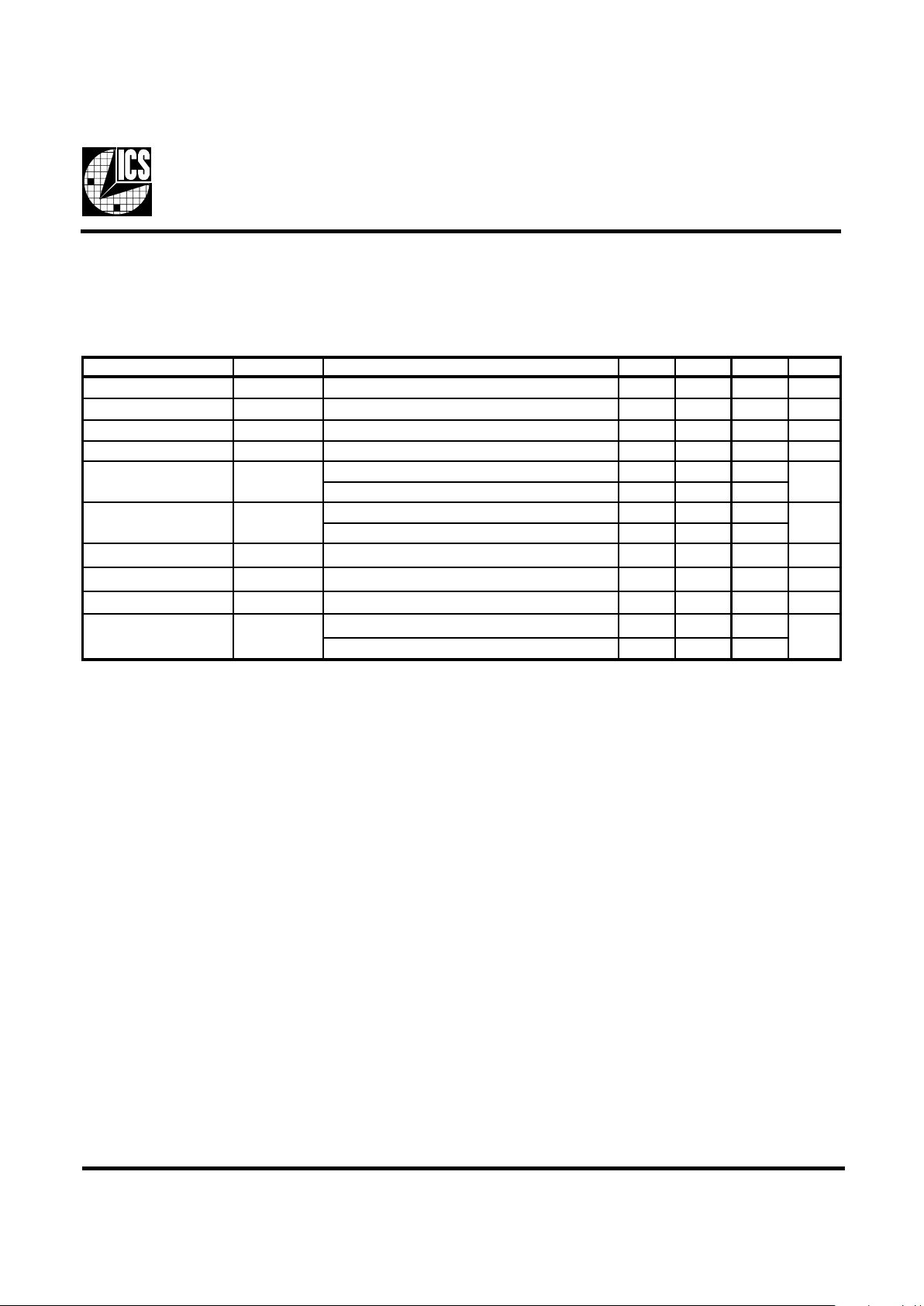
Electrical Characteristics - REF, 24_48MHz, 48MHz
TA = 0 - 70C; VDD = 3.3 V +/-5%; CL = 10-2 0 pF (unless otherwise specified)
PARAMETER SYMBOL CONDITIONS MIN TYP MAX UNITS
Output Impedance
1
R
DSP5
VO = VDD*(0.5) 20 60
Ω
Output Impedance
1
R
DSN5
VO = VDD*(0.5) 20 60
Ω
Output High Voltage V
OH5
IOH = -1 mA 2.4 V
Output Low Vo ltage V
OL5
IOL = 1 mA 0.4 V
V
OH @ MIN
= 1.0 V -23
V
OH @ MAX
= 3.135 V -29
V
OL @ MIN
= 1.95 V 29
V
OL @ MAX
= 0.4 V 27
Rise Time
1
t
r5
VOL = 0.4 V, VOH = 2.4 V 0.4 2 4 ns
Fall Time
1
t
f5
VOH = 2.4 V, VOL = 0.4 V 0.4 2 4 ns
Duty Cycle
1
d
t5
VT = 1.5 V 45 53 55 %
V
T
= 1.5 V, Fixed clocks 200 500
V
T
= 1.5 V, Ref clocks
1032 1250
1
Guaranteed by design, not 100% tested in production.
Jitter, cycle-to-cycle
1
t
jcyc-cyc5
ps
Output High Current
I
OH5
mA
Output Low Curr e nt
I
OL5
mA
Page 14
14
ICS94206
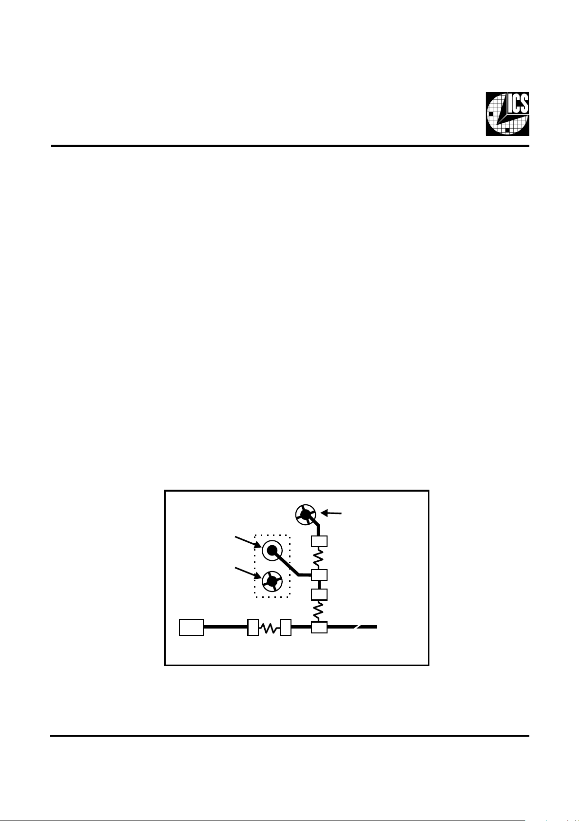
Fig. 1
Shared Pin Operation Input/Output Pins
The I/O pins designated by (input/output) on the ICS94206
serve as dual signal functions to the device. During initial
power-up, they act as input pins. The logic level (voltage) that
is present on these pins at this time is read and stored into a 5bit internal data latch. At the end of Power -On reset, (see AC
characteristics for timing values), the device changes the
mode of operations for these pins to an output function. In this
mode the pins produce the specified buffered clocks to external
loads.
To program (load) the internal configuration register for these
pins, a resistor is connected to either the VDD (logic 1) power
supply or the GND (logic 0) voltage potential. A 10 Kilohm
(10K) resistor is used to provide both the solid CMOS
programming voltage needed during the power-up
programming period and to provide an insignificant load on
the output clock during the subsequent operating period.
Via to
VDD
Clock trace to load
Series Term. Res.
Programming
Header
Via to Gnd
Device
Pad
2K
8.2K
Figure 1 shows a means of implementing this function when
a switch or 2 pin header is used. With no jumper is installed
the pin will be pulled high. W ith the jumper in place the pin
will be pulled low. If programmability is not necessary, than
only a single resistor is necessary . The programming resistors
should be located close to the series termination resistor to
minimize the current loop area. It is more important to locate
the series termination resistor close to the driver than the
programming resistor.
Page 15
15
ICS94206
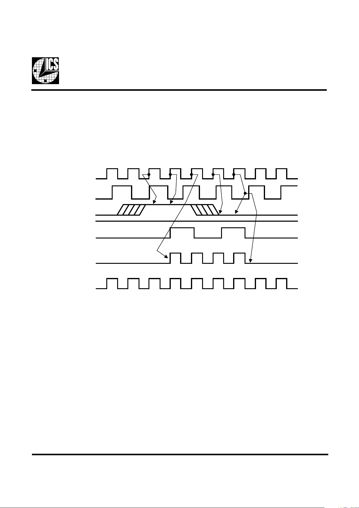
CLK_STOP# Timing Diagram
CLK_STOP# is an asychronous input to the clock synthesizer. It is used to turn off the CPU clocks for low power operation.
CLK_STOP# is synchronized by the ICS94206. The minimum that the CPU clock is enabled (CLK_STOP# high pulse) is 100 CPU
clocks. All other clocks will continue to run while the CPU clocks are disabled. The CPU clocks will always be stopped in a low state
and start in such a manner that guarantees the high pulse width is a full pulse. CPU clock on latency is less than 4 CPU clocks and
CPU clock off latency is less than 4 CPU clocks.
Notes:
1. All timing is referenced to the internal CPU clock.
2. CLK_STOP# is an asynchronous input and metastable conditions may exist. This signal is synchronized
to the CPU clocks inside the ICS94206.
3. IOAPIC output is Stopped Glitch Free by CLK_STOP# going low.
4. SDRAM-F output is controlled by Buffer in signal, not affected by the ICS94206
CLK_STOP# signal. SDRAM's are controlled as shown.
5. All other clocks continue to run undisturbed.
PCICLK
SDRAM
CPUCLK
CPUCLK _F
SDRAM_F
IOAPIC
PCI_STOP# (High)
CLK_STOP#
INTERNAL
CPUCLK
Page 16
16
ICS94206
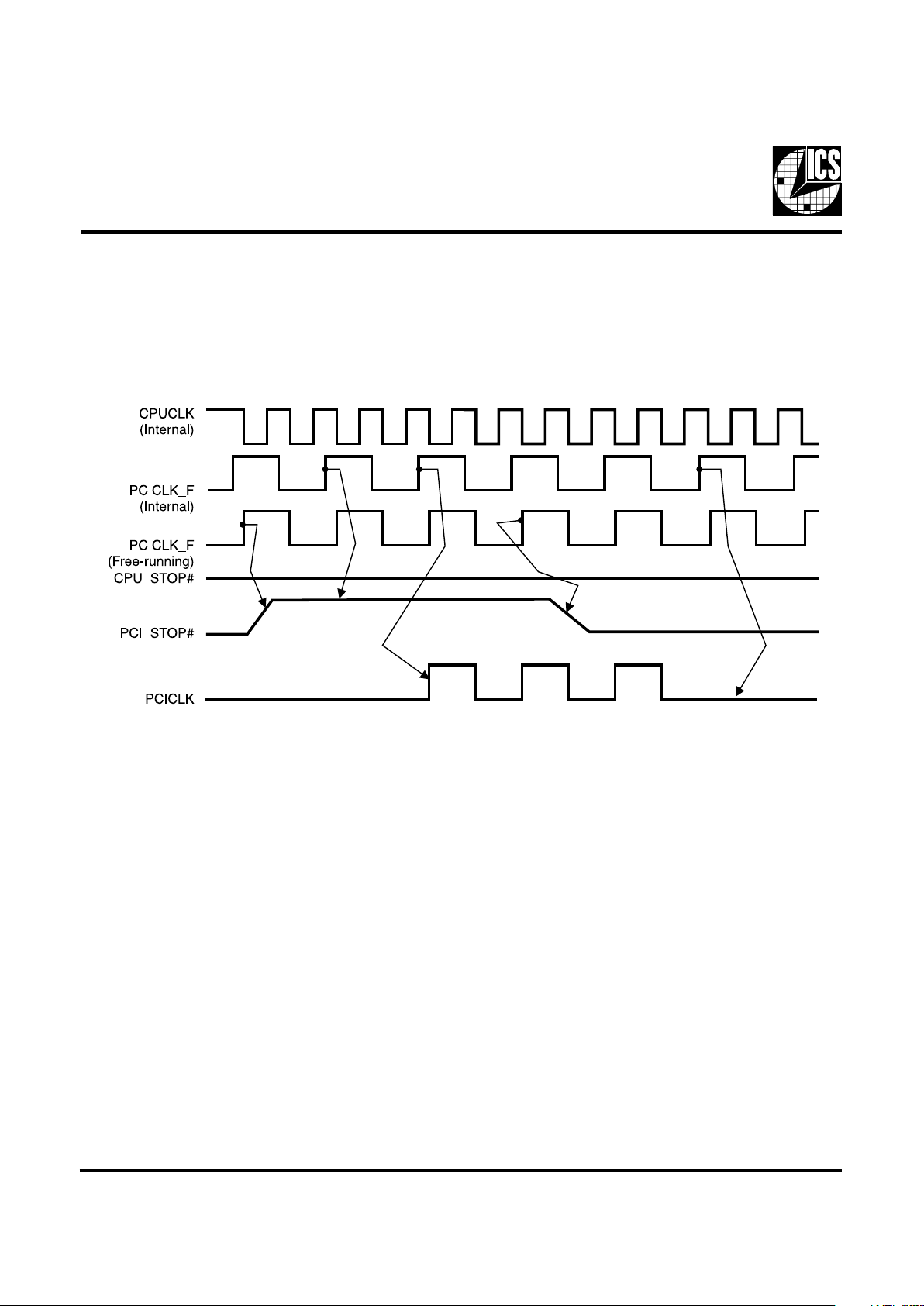
PCI_STOP# Timing Diagram
PCI_STOP# is an asynchronous input to the ICS94206. It is used to turn off the PCICLK clocks for low power operation. PCI_STOP#
is synchronized by the ICS94206 internally. The minimum that the PCICLK clocks are enabled (PCI_STOP# high pulse) is at least
10 PCICLK clocks. PCICLK clocks are stopped in a low state and started with a full high pulse width guaranteed. PCICLK clock on
latency cycles are only one rising PCICLK clock off latency is one PCICLK clock.
Notes:
1. All timing is referenced to the Internal CPUCLK (defined as inside the ICS94206 device.)
2. PCI_STOP# is an asynchronous input, and metastable conditions may exist. This signal is required to be synchronized
inside the ICS94206.
3. All other clocks continue to run undisturbed.
4. CPU_STOP# is shown in a high (true) state.
Page 17
17
ICS94206
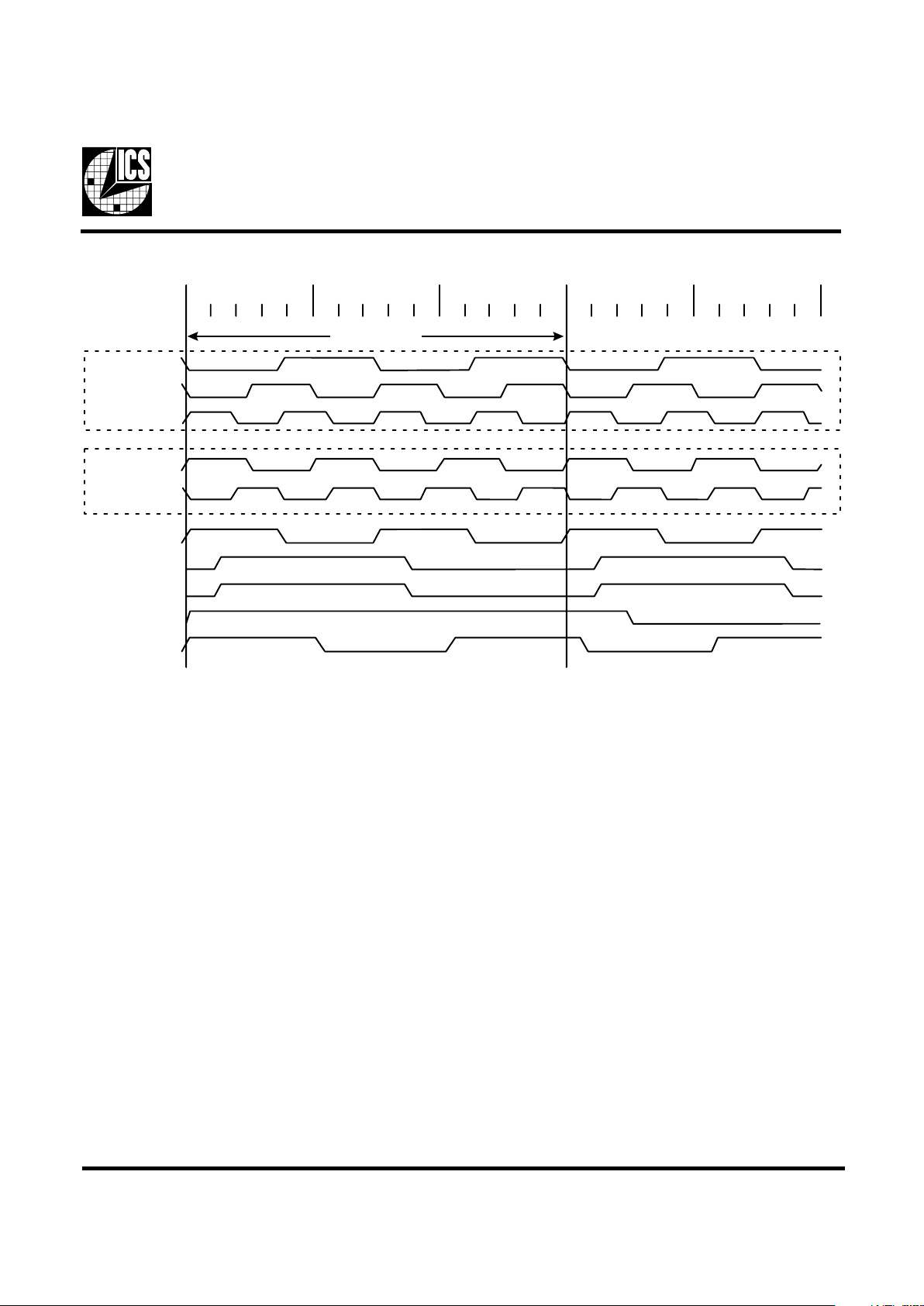
Group Offset Waveforms
Cycle Repeats
0ns
CPU 66MHz
CPU 100MHz
CPU 133MHz
SDRAM 133MHz
SDRAM 100MHz
3.5V 66MHz
PCI 33MHz
APIC 33MHz
REF 14.318MHz
USB 48MHz
10ns 20ns 30ns 40ns
Page 18
18
ICS94206
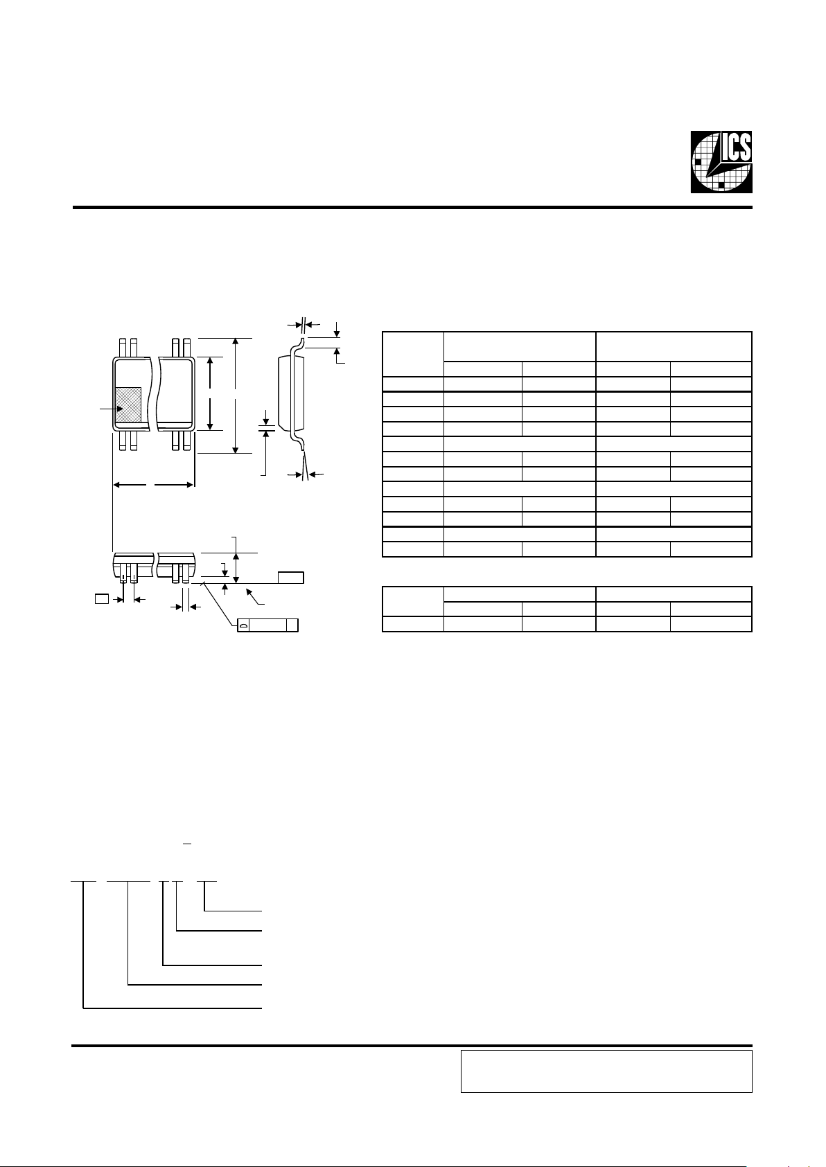
Ordering Information
ICS94206yF-T
Designation for tape and reel packaging
Package Type
F=SSOP
Revision Designator (will not correlate with datasheet revision)
Device Type
Prefix
ICS, AV = Standard Device
Example:
ICS XXXX y F - T
INDEX
AREA
INDEX
AREA
12
1 2
N
D
h x 45°
h x 45°
E1
E
SEATING
PLANE
SEATING
PLANE
A1
A
e
-C-
- C -
b
.10 (.004) C
.10 (.004) C
c
L
300 mil SSOP Package
MIN MAX MIN MAX
A 2.41 2.80 .095 .110
A1 0.20 0.40 .008 .016
b 0.20 0.34 .008 .0135
c 0.13 0.25 .005 .010
D
E 10.03 10.68 .395 .420
E1 7.40 7.60 .291 .299
e
h 0.38 0.64 .015 .025
L 0.50 1.02 .020 .040
N
α
0° 8° 0° 8°
MIN MAX MIN MAX
48 15.75 16.00 .620 .630
10-0034
SYMBOL
In Millimeters In Inches
COMMON DIMENSIONS COMMON DIMENSIONS
SEE VARIATIONS SEE VARIATIONS
0.635 BASIC 0.025 BASIC
Reference Doc.: JEDEC Publication 95, MO-118
VARIATIONS
SEE VARIATIONS SEE VARIATIONS
N
D mm. D (inch)
ICS reserves the right to make changes in the device data identified in
this publication without further notice. ICS advises its customers to
obtain the latest version of all device data to verify that any
information being relied upon by the customer is current and accurate.
 Loading...