

Page 1
Integrated
Circuit
Systems, Inc.
ICS94203
94203 Rev B 02/13/01
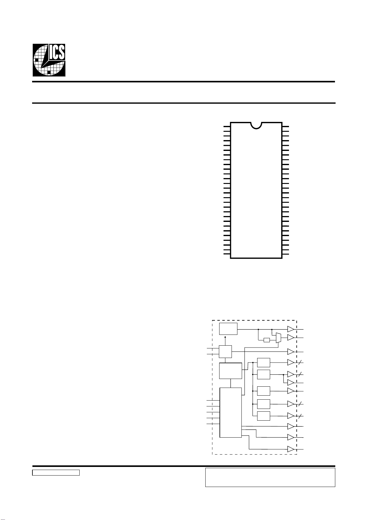
Pin Configuration
Recommended Application:
810/810E and Solano (815) type chipset
Output Features:
• 2 - CPUs @ 2.5V
• 13 - SDRAM @ 3.3V
• 3 - 3V66 @ 3.3V
• 7 - PCI @3.3V
• 1 - 24/48MHz@ 3.3V
• 1 - 48MHz @ 3.3V fixed
• 1 - REF @3.3V, 14.318MHz
Features:
• Programmable ouput frequency
• Gear ratio change detection
• Real time system reset output
• Spread spectrum for EMI control
with programmable spread percentage
• Watchdog timer technology to reset system
if over-clocking causes malfunction.
• Support power management through PD#.
• Uses external 14.318MHz crystal
• FS pins for frequency select
Key Specifications:
• CPU Output Jitter: <250ps
• IOAPIC Output Jitter: <500ps
• 48MHz, 3V66, PCI Output Jitter: <500ps
• CPU Output Skew: <175ps
• PCI Output Skew: <500ps
• 3V66 Output Skew <175ps
• For group skew timing, please refer to the
Group Timing Relationship Table.
Programmable System Frequency Generator for PII/III™
56-Pin 300 mil SSOP
1. These pins will have 1.5 to 2X drive strength.
* 120K ohm pull-up to VDD on indicated inputs.
VDDA
GNDA
X1
X2
GND3V66
VDD3V66
3V66-0
3V66-1
3V66-2
VDDPCI
GNDPCI
*FS0/PCICLK0
*FS1/PCICLK1
*SEL24_48#/PCICLK2
GNDPCI
VDDPCI
PCICLK3
PCICLK4
PCICLK5
PCICLK6
RATIO_0
PD#
SCLK
S DATA
VDD48
GND48
*FS2/24_48MHz
*FS3/48MHz
1
1
1
1
REF/FS4*
VDDLAPIC
IOAPIC0
VDDLCPU
GNDLCPU
CPUCLK0
CPUCLK1
GNDSDR
VDDSDR
SDRAM0
SDRAM1
SDRAM2
SDRAM3
VDDSDR
GNDSDR
SDRAM4
SDRAM5
SDRAM6
SDRAM7
SDRAM_F
GNDSDR
VDDSDR
SDRAM8
SDRAM9
SDRAM10
SDRAM11
RESET#
RATIO_1
1
1
ICS94203
1
2
3
4
5
6
7
8
9
10
11
12
13
14
15
16
17
18
19
20
21
22
23
24
25
26
27
28
56
55
54
53
52
51
50
49
48
47
46
45
44
43
42
41
40
39
38
37
36
35
34
33
32
31
30
29
Block Diagram
PLL2
PLL1
Spread
Spectrum
48MHz
24_48MHz
CPUCLK (1:0)
2
12
7
3
SDRAM (11:0)
IOAPIC
PCICLK (6:0)
SDRAM_F
3V66 (2:0)
RESET#
RATIO_0
RATIO_1
X1
X2
XTAL
OSC
CPU
DIVDER
SDRAM
DIVDER
IOAPIC
DIVDER
PCI
DIVDER
3V66
DIVDER
FS(4:0)
PD#
SEL24_48#
S DATA
SCLK
Control
Logic
Config.
Reg.
/ 2
REF
Power Groups
VDDA, GNDA = Core PLL, Xtal
VDD48, GND48 = 48MHz, Fixed PLL
ICS reserves the right to make changes in the device data identified in
this publication without further notice. ICS advises its customers to
obtain the latest version of all device data to verify that any
information being relied upon by the customer is current and accurate.
Page 2
2
ICS94203
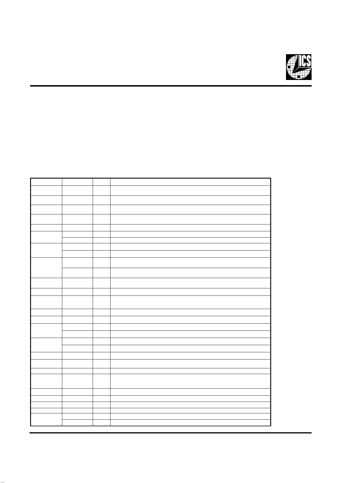
General Description
Pin Configuration
The ICS94203 is a single chip clock solution for desktop designs using the 810/810E and Solano style chipset. It provides all necessary
clock signals for such a system.
The ICS94203 belongs to ICS new generation of programmable system clock generators. It employs serial programming I
2
C interface
as a vehicle for changing output functions, changing output frequency, configuring output strength, configuring output to output skew ,
changing spread spectrum amount, changing group divider ratio and dis/enabling individual clocks. This device also has ICS
propriety 'Watchdog Timer' technology which will reset the frequency to a safe setting if the system become unstable from over
clocking.
Spread spectrum typically reduces system EMI by 7dB to 8dB. This simplifies EMI qualification without resorting to board design
iterations or costly shielding.
REBMUNNIPEMANNIPEPYTNOITPIRCSED
,52,61,01,6,1
84,34,53
DDVRWPylppusrewopV3.3
3
1XNI
kcabdeefdna)Fp33(pacdaollanretnisah,tupnilatsyrC
2Xmorfrotsiser
4
2XTUO)Fp33(pacdaollanretnisaH.zHM813.41yllanimon,tuptuolatsyrC
,62,51,11,5,2
94,24,63
DNGRWPylppusV3.3rofsnipdnuorG
7,8,9
]0:2[66V3TUOBUHrofstuptuokcolczHM66dexiFV3.3
21
0KLCICP
1
TUOSKLCUPCsuonorhcnyShtiw,tuptuokcolcICPV3.3
0SFNI.norewoptadehctaltupnI.tibtcelesycneuqerftupnicigoL
31
1KLCICP
1
TUOSKLCUPCsuonorhcnyShtiw,tuptuokcolcICPV3.3
1SFNI.norewoptadehctaltupnI.tibtcelesycneuqerftupnicigoL
41
#84_42LESNI72niprofniptcelesycneuqerfzHM84/42
2KLCICPTUOSKLCUPCsuonorhcnyShtiw,tuptuokcolcICPV3.3
71,81,91,02
]3:6[KLCICPTUOSKLCUPCsuonorhcnyShtiw,stuptuokcolcICPV3.3
12
0_OITARTUO .rossecorpehtmorfyllanigroslangis0LESBehtgnicalper,tespihcottuptuO
22
#DPNI
ehT.etatsrewopwolaotniecivedehtnwodrewopotdesuniptupniwolevitcasuonorhcnysA
rewopehtfoycnetalehT.deppotseralatsyrcehtdnaOCVehtdnadelbasideraskcolclanretni
.sm3nahtretaergebtonlliwnwod
32
KLCSNIIfotupnikcolC
2
tupniC
42
ATADSO/IIroftupniataD
2
.tupnilairesC
72
2SFNI.norewoptadehctaltupnI.tibtcelesycneuqerftupnicigoL
zHM84_42TUO.zHM42sitluafeDtuptuozHM84_42V3.3
82
3SFNI.norewoptadehctaltupnI.tibtcelesycneuqerftupnicigoL
zHM84TUO.BSUroftuptuokcolczHM84dexiFV3.3
92
1_OITARTUO .rossecorpehtmorfyllanigroslangis1ESBehtgnicalper,tespihcottuptuO
03
TESERTUO
.tuoemitremmitgodhctawroegnahcoitarycneuqerfroflangistesermetsysemitlaeR
.wolevitcasilangissihT
73
F_MARDSTUOIhguorhtffodenrutebnactuptuoMARDSV3.3
2
C
,43,33,23,13
,14,04,93,83
74,64,54,44
]0:11[MARDSTUOIhguorhtffodenrutebnacstuptuoMARDSllA.tuptuoV3.3
2
C
15,05]0:1[KLCUPCTUO.snipSFmorfdeviredycneuqerftuptuO.tuptuokcolcsubtsoHV5.2
25LDNGRWPCIPA&UPCrofylppusrewopV5.2rofdnuorG
55,35LDDVRWPCIPAOI,UPCrofylppyusrewopV5.2
45CIPAOITUO.zHM76.61tagninnurstuptuokcolcV5.2
65
4SFNI.norewoptadehctaltupnI.tibtcelesycneuqerftupnicigoL
FER
1
TUO.tuptuokcolcecnereferzHM813.41,V3.3
Page 3
3
ICS94203
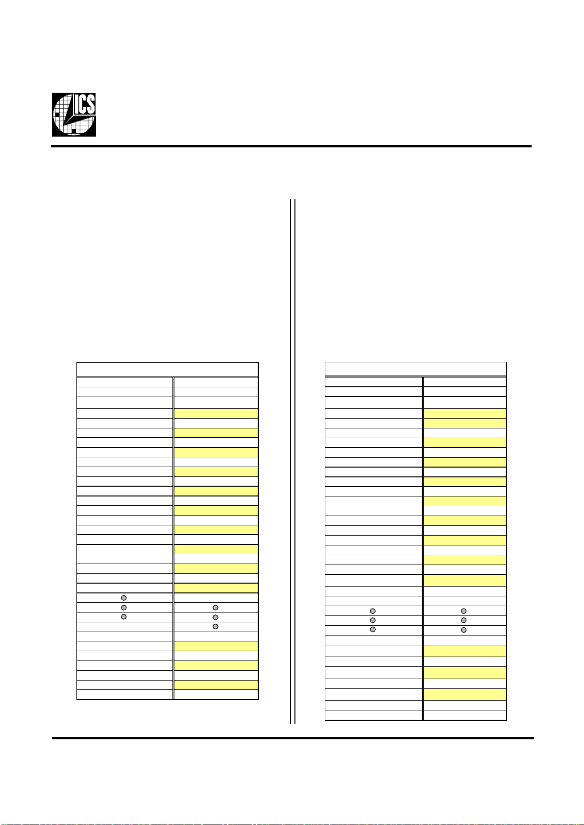
General I2C serial interface information for the ICS94203
How to Write:
• Controller (host) sends a start bit.
• Controller (host) sends the write address D2
(H)
• ICS clock will acknowledge
• Controller (host) sends a dummy command code
• ICS clock will acknowledge
• Controller (host) sends a dummy byte count
• ICS clock will acknowledge
• Controller (host) starts sending Byte 0 through Byte 28
(see Note 2)
• ICS clock will acknowledge each byte one at a time
• Controller (host) sends a Stop bit
How to Read:
• Controller (host) will send start bit.
• Controller (host) sends the read address D3
(H)
• ICS clock will acknowledge
• ICS clock will send the byte count
• Controller (host) acknowledges
• ICS clock sends Byte 0 through byte 6 (default)
• ICS clock sends Byte 0 through byte X (if X
(H)
was
written to byte 6).
• Controller (host) will need to acknowledge each byte
• Controller (host) will send a stop bit
Controll e r (Host)
ICS (Slave/Receiver)
Start Bit
Address D2
(H)
ACK
Dumm y Comm an d Cod e
ACK
Dumm y B y te Count
ACK
Byte 0
ACK
Byte 1
ACK
Byte 2
ACK
Byte 3
ACK
Byte 4
ACK
Byte 5
ACK
Byte 6
ACK
Byte 26
ACK
Byte 27
ACK
Byte 28
ACK
Stop Bit
How to Write:
*See notes on the following page.
Controller (Host)
ICS (Sla ve/Receiver)
Start Bit
Addres s D3
(H)
ACK
Byte Count
ACK
Byte 0
ACK
Byte 1
ACK
Byte 2
ACK
Byte 3
ACK
Byte 4
ACK
Byte 5
ACK
Byte 6
ACK
If 7
H
has been wri t ten to B 6
Byte 7
ACK
If 1A
H
has been wri t ten to B6
Byte26
ACK
If 1B
H
has been wri t ten to B6
Byte 27
ACK
If 1C
H
has been wri t ten to B6
Byte 28
ACK
Stop Bit
How to Read:
Page 4
4
ICS94203
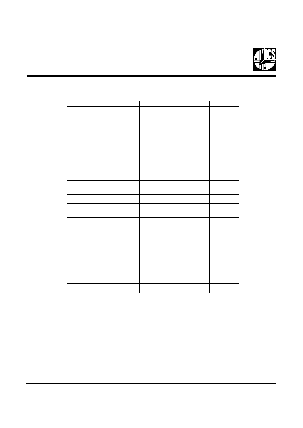
1. The ICS clock generator is a slave/receiver, I2C component. It can read back the data stored in the latches for verification.
Readback will support standard SMBUS controller protocol. The number of bytes to readback is defined by writing to
byte 6.
2. When writing to byte 14 - 15, byte 16 - 17 and byte 18 - 20, they must be written as a set. If for example, only byte
14 is written but not 15, neither byte 14 or 15 will load into the receiver.
3. The data transfer rate supported by this clock generator is 100K bits/sec or less (standard mode)
4. The input is operating at 3.3V logic levels.
5. The data byte format is 8 bit bytes.
6. To simplify the clock generator I
2
C interface, the protocol is set to use only Block-Writes from the controller. The bytes
must be accessed in sequential order from lowest to highest byte with the ability to stop after any complete byte has been
transferred. The Command code and Byte count shown above must be sent, but the data is ignored for those two bytes.
The data is loaded until a Stop sequence is issued.
7. At power-on, all registers are set to a default condition, as shown.
Notes:
Regi s ter Name Byte Descript ion Pwd Default
Functionalit y & Frequency Sel ect
Register
0
Output frequenc y, hardware / I
2
C frequency
select, spread spectrum & output enable
cont rol register.
See individual byt e
description
Output Cont rol Registers 1-5 Active / i nactive output control registers.
See individual byt e
description
By t e Count Read B ac k Register 6
Writ i ng t o t his regist er will c onfigure by t e
count and how m any byt e wi l l be read back.
Do not write 00
H
to this byte.
06
H
Latc hed Input s Read Back
Register
7
The invers e of t he l atched inputs level could
be read back from t his regis ter.
See individual byt e
description
Watchdog Control Regi sters 8 Bit[6:0]
Wat c hd og enable, wat c hdog s t at us and
programmable 'safe' frequency ' c an be
configured in t his regis ter.
000,0000
VCO Control Selection Bit 8 Bit[7]
This bit s el ec t whet her t he out put frequency
is control by hardware/byt e 0 configurations
or byt e 14& 15 program m i ng.
0
Watchdog Timer Count Register 9
Writ i ng t o t his regist er will c onfigure t he
number of seconds for the watchdog t im er
to reset.
FF
H
ICS Reserved Register 10
This is an unus ed regi s t er. W ri t ing to this
regist er wil l no t affect device funct i onal i ty.
00
H
Device ID, Vendor ID & Revision ID
Registers
11-12
By t e 11 bi t[3:0] is ICS vendor id - 0001.
Other bits in these 2 regis ters des i gnate
device revision ID of this part .
See individual byt e
description
ICS Reserved Register 13
Don't write int o this register, writing 1's will
caus e m al function.
00
H
VCO Frequenc y Control Registers 14-15
These registers control the di viders rat io
into t he phase detec tor and thus control t he
VCO outpu t frequenc y.
Depended on
hardware/byte 0
configuration
Spread Spec t rum Cont rol
Registers
16-17
These registers control the spread
percentage am ount.
Depended on
hardware/byte 0
configuration
Output Di viders Cont rol Regi sters 18-20
Changing bits i n t hes e registers res ul t in
frequency di vider ratio changes. Inc orrec t
configuration of group output divider ratio
can cause system malfunction.
Depended on
hardware/byte 0
configuration
Group Sk ews Control Regis ters 21
Increment or dec rem ent t he group s k ew
amount as compared to the initial s kew.
See individual byt e
description
Output Ri se/Fall Tim e S elect
Registers
22
These register will control the group rise
and fall ti m e.
See individual byt e
description
Brief I2C registers description for ICS94203
Programmable System Frequency Generator
Page 5
5
ICS94203
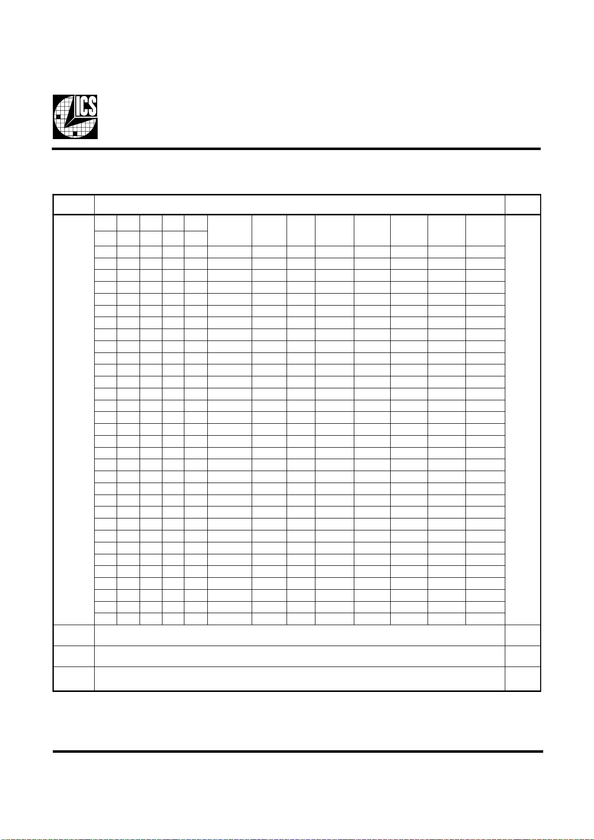
Byte 0: Functionality and frequency select register (Default=0)
Notes:
1.
Default at power-up will be for latched logic inputs to define frequency, as displayed by Bit 3.
tiB
noitpircseD
DWP
tiB
)4:7,2(
2tiB7tiB6tiB5tiB4tiB
FER/OCV
rediviD
OCV
zHM
/OCV
UPC
KLCUPC
zHM
MARDS
zHM
66V3
zHM
KLCICP
zHM
CIPAOI
zHM
1etoN
4SF3SF2SF1SF0SF
00000 31/26317.893654.6656.9934.6612.3316.61
00001 41/25300.063600.0600.0900.0600.0300.51
00010 81/40519.004608.6602.00108.6604.3307.61
00011 11/51320.014633.8605.20133.8671.4380.71
00100 51/04400.024600.0700.50100.0700.5305.71
00101 41/04400.054600.5705.21100.5705.7357.81
00110 51/30541.084600.0800.02100.0800.0400.02
00111 9/31359.794600.3805.42100.3805.1457.02
01000 73/51592.991256.9956.9934.6612.3316.61
01001 04/74492.061200.0800.0833.3576.6233.31
01010 73/81554.0022 32.00132.00148.6614.3307.61
01011 13/64400.6022 00.30100.30176.8633.4371.71
01100 33/48400.0122 00.50100.50100.0700.5305.71
01101 33/70589.9122 00.01100.01133.3776.6333.81
01110 23/41599.9222 00.51100.51176.6733.8371.91
01111 11/16460.0062 00.00200.00200.00100.0500.52
10000 31/26317.8933 68.23168.23134.6612.3316.61
10001 51/30541.0843 00.06100.06100.0800.0400.02
10010 81/40519.0043 46.33146.33128.6614.3307.61
10011 71/88420.1143 00.73100.73105.8652.4331.71
10100 51/04400.0243 00.04100.04100.0700.5305.71
10101 31/59350.5343 00.54100.54105.2752.6331.81
10110 41/04400.0543 00.05100.05100.5705.7357.81
10111 51/30541.0843 00.06100.06100.0800.0400.02
11000 31/26317.8933 09.23156.9939.6612.3316.61
11001 51/30541.0843 00.06100.00100.0800.0400.02
11010 81/40519.0043 46.33132.00128.6614.337.61
11011 71/88420.1143 00.73157.20105.8652.4331.71
11100 51/04400.0243 00.04100.50100.0700.5305.71
11101 31/59350.5343 00.54157.80105.2752.6331.81
11110 41/04400.0543 00.05105.21100.5705.7357.81
11111 51/30541.0843 00.06100.02100.0800.0400.02
3tiB
stupnidehctal,tceleserawdrahybdetcelessiycneuqerF-0
4:7,2tiBybdetcelessiycneuqerF-1
0
1tiB
lamroN-0
daerpSretneC%53.0±elbanemurtcepsdaerpS-1
1
0tiB
gninnuR-0
stuptuollaetatsirT-1
0
Page 6
6
ICS94203
Notes:
1. Inactive means outputs are held LOW and are disabled from switching. These outputs are designed to be configured at
power-on and are not expected to be configured during the normal modes of operation.
2. PWD = Power on Default
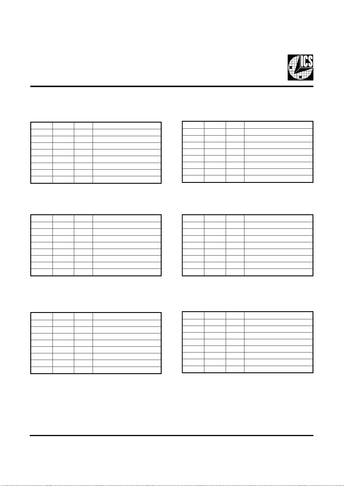
Byte 1: Output Control Register
(1 = enable, 0 = disable)
Notes:
1. Inactive means outputs are held LOW and are disabled from switching. These outputs are designed to be configured at
power-on and are not expected to be configured during the normal modes of operation.
2. PWD = Power on Default
Byte 3: Output Control Register
(1 = enable, 0 = disable)
Byte 2: Output Control Register
(1 = enable, 0 = disable)
Byte 4: Output Control Register
(1 = enable, 0 = disable)
Byte 5: Output Control Register
(1 = enable, 0 = disable)
Byte 6: Byte Count Read Back Register
Note: Writing to this register will configure byte count and
how many bytes will be read back, default is 6 bytes.
tiB#niPDWPnoitpircseD
7tiB831 7MARDS
6tiB931 6MARDS
5tiB041 5MARDS
4tiB141 4MARDS
3tiB441 3MARDS
2tiB541 2MARDS
1tiB641 1MARDS
0tiB741 0MARDS
tiB#niPDWPnoitpircseD
7tiB91 2_66V3
6tiB71 0_66V3
5tiB81 1_66V3
4tiB651FER
3tiB451 0CIPAOI
2tiB-X devreseR
1tiB051 1KLCUPC
0tiB151 0KLCUPC
tiB#niPDWPnoitpircseD
7tiB-0 )etoN(devreseR
6tiB-0 )etoN(devreseR
5tiB-0 )etoN(devreseR
4tiB-0 )etoN(devreseR
3tiB-0 )etoN(devreseR
2tiB-1 )etoN(devreseR
1tiB-1 )etoN(devreseR
0tiB-0 )etoN(devreseR
tiB#niPDWPnoitpircseD
7tiB-1 )devreseR(
6tiB-1 )devreseR(
5tiB-1 )devreseR(
4tiB-1 )devreseR(
3tiB131 11MARDS
2tiB231 01MARDS
1tiB331 9MARDS
0tiB431 8MARDS
tiB#niPDWPnoitpircseD
7tiB-0 devreseR
6tiB021 6KLCICP
5tiB911 5KLCICP
4tiB811 4KLCICP
3tiB711 3KLCICP
2tiB411 2KLCICP
1tiB311 1KLCICP
0tiB211 0KLCICP
tiB#niPDWPnoitpircseD
7tiB
-1 )devreseR(
6tiB
-1 )devreseR(
5tiB
-1 )devreseR(
4tiB
721 zHM84_42
3tiB
-1 )devreseR(
2tiB
821 zHM84
1tiB
-1 )devreseR(
0tiB
731 F_MARDS
Page 7
7
ICS94203
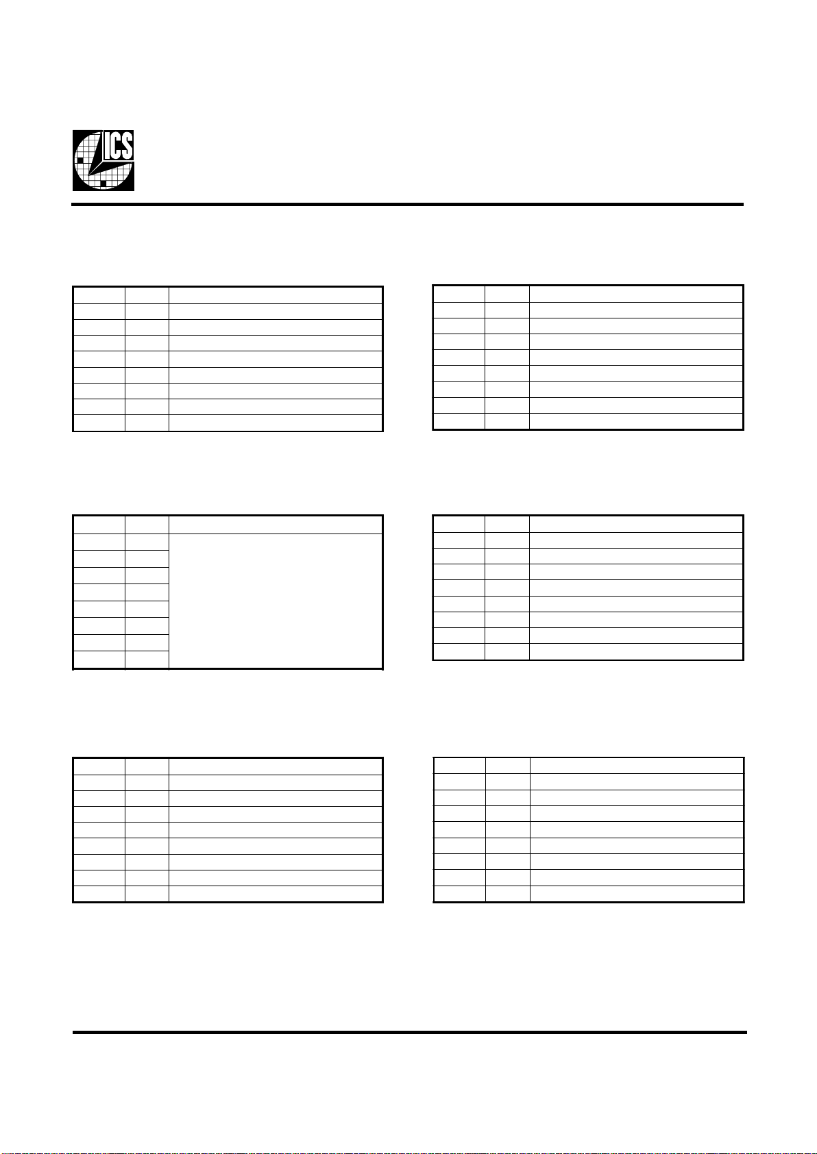
Byte 7: Latch Inputs Readback Register
Byte 9: Watchdog Timer Count Register
Byte 8: VCO Control Selection Bit &
Watchdog Timer Control Register
Byte 10: ICS Reserved Register
Byte 11: Vender ID & Device ID Register
Byte 12: Revision ID Register
Note: FS values in bit [0:4] will correspond to Byte 0 FS
values. Default safe frequency is same as 00000 entry in
byte0.
Note: This is an unused register. Writing to this register will
not affect device performance or functionality.
Note: ICS Vendor ID is 0001 as in Number 1 in
frequency generation.
Notes:
1. PWD = Power on Default
tiBDWPnoitpircseD
7tiB0 qerf51&41B=1/qerf0B/wH=0
6tiB0 elbane=1/elbasid=0elbanEDW
5tiB0 mrala=1/lamron=0sutatSDW
4tiB0 4SF,ycneuqerFefaSDW
3tiB0 3SF,ycneuqerFefaSDW
2tiB0 2SF,ycneuqerFefaSDW
1tiB0 1SF,ycneuqerFefaSDW
0tiB0 0SF,ycneuqerFefaSDW
tiBDWPnoitpircseD
7tiB0 )devreseR(
6tiB0 )devreseR(
5tiB0 )devreseR(
4tiB0 )devreseR(
3tiB0 )devreseR(
2tiB0 )devreseR(
1tiB0 )devreseR(
0tiB0 )devreseR(
tiBDWPnoitpircseD
7tiBX DInoisiveR
6tiBX DInoisiveR
5tiBX DInoisiveR
4tiBX DInoisiveR
3tiBX DInoisiveR
2tiBX DInoisiveR
1tiBX DInoisiveR
0tiBX DInoisiveR
tiBDWPnoitpircseD
7tiB0 )devreseR(
6tiB0 )devreseR(
5tiBX #)#84_42LES(
4tiBX#4SF
3tiBX#3SF
2tiBX#2SF
1tiBX#1SF
0tiBX#0SF
tiBDWPnoitpircseD
7tiB0 DIeciveD
6tiB0 DIeciveD
5tiB1 DIeciveD
4tiB1 DIeciveD
3tiB0 DIrodneV
2tiB0 DIrodneV
1tiB0 DIrodneV
0tiB1 DIrodneV
Note: Device ID and Revision ID values will be based on
individual device and its revision.
tiBDWPnoitpircseD
7tiB0
esehtfonoitatneserperlamicedehT
ehtsm092otdnopserrocstib8
tierofebtiawlliwremitgodhctaw
ehtteserdnaedommralaotseog
tluafeD.gnittesefasehtotycneuqerf
4.4=sm092X51sipurewopta
tonseodremitsiht,etoN.sdnoces
)03nip(langis#TESERehtlortnoc
.egnahcoitarycneuqerfehtfoesacni
6tiB0
5tiB0
4tiB0
3tiB1
2tiB1
1tiB1
0tiB1
Page 8
8
ICS94203
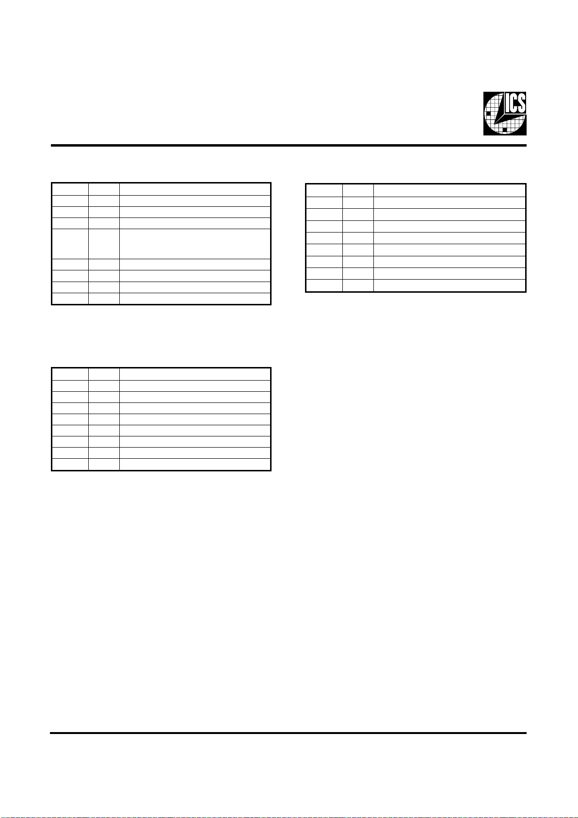
Byte 13: ICS Reserved Register
Byte 15: VCO Frequency Control Register
Note: The decimal representation of these 9 bits (Byte 15 bit
[7:0] & Byte 14 bit [7] ) + 8 is equal to the VCO divider value.
For example if VCO divider value of 36 is desired, user need
to program 36 - 8 = 28, namely, 0, 00011100 into byte 15 bit
& byte 14 bit 7.
Note: DON'T write a '1' into this register, it will
cause malfunction.
Byte 14: VCO Frequency Control Register
Note: The decimal representation of these 7 bits (Byte 14
[6:0]) + 2 is equal to the REF divider value .
VCO Programming Constrains
VCO Frequency ...................... 150MHz to 500MHz
VCO Divider Range ................ 8 to 519
REF Divider Range ................. 2 to 129
Phase Detector Stability .......... 0.3536 to 1.4142
Useful Formula
VCO Frequency = 14.31818 x VCO/REF divider value
Phase Detector Stabiliy = 14.038 x (VCO divider value)
-0.5
tiBDWPnoitpircseD
7tiBX 8tiBrediviDOCV
6tiBX 7tiBrediviDOCV
5tiBX 6tiBrediviDOCV
4tiBX 5tiBrediviDOCV
3tiBX 4tiBrediviDOCV
2tiBX 3tiBrediviDOCV
1tiBX 2tiBrediviDOCV
0tiBX 1tiBrediviDOCV
tiBDWPnoitpircseD
7tiBX 0tiBrediviDOCV
6tiBX 6tiBrediviDFER
5tiBX 5tiBrediviDFER
4tiBX 4tiBrediviDFER
3tiBX 3tiBrediviDFER
2tiBX 2tiBrediviDFER
1tiBX 1tiBrediviDFER
0tiBX 0tiBrediviDFER
tiBDWPnoitpircseD
7tiB0 )devreseR(
6tiB0 )devreseR(
5tiB0 )devreseR(
4tiB0
tcelesesabremit0W
sm092=0
sm5.0=1
3tiB0 )devreseR(
2tiB0 )devreseR(
1tiB0 )devreseR(
0tiB0 )devreseR(
To program the VCO frequency for over-clocking.
0. Before trying to program our clock manually, consider using ICS provided software utilities for easy programming.
1. Select the frequency you want to over-clock from with the desire gear ratio (i.e. CPU:SDRAM:3V66:PCI ratio) by writing to
byte 0, or using initial hardware power up frequency .
2. Write 0001, 0111 (17H) to byte 6 for readback of 23 bytes (byte 0-22).
3. Read back byte 16-24 and copy values in these registers.
4. Re-initialize the write sequence.
5. Write a '1' to byte 8 bit 7 indicating you want to use byte 14 and 15 to control the VCO frequency.
6. Write to byte 14 & 15 with the desired VCO & REF divider values.
7. Write to byte 16 to 22 with the values you copy from step 3. This maintains the output divider mux controls the same gear ratio.
8. The above procedure is only needed when changing the VCO for the 1st pass. If VCO frequency needed to be changed again,
user only needs to write to byte 14 and 15 unless the system is to reboot.
Page 9
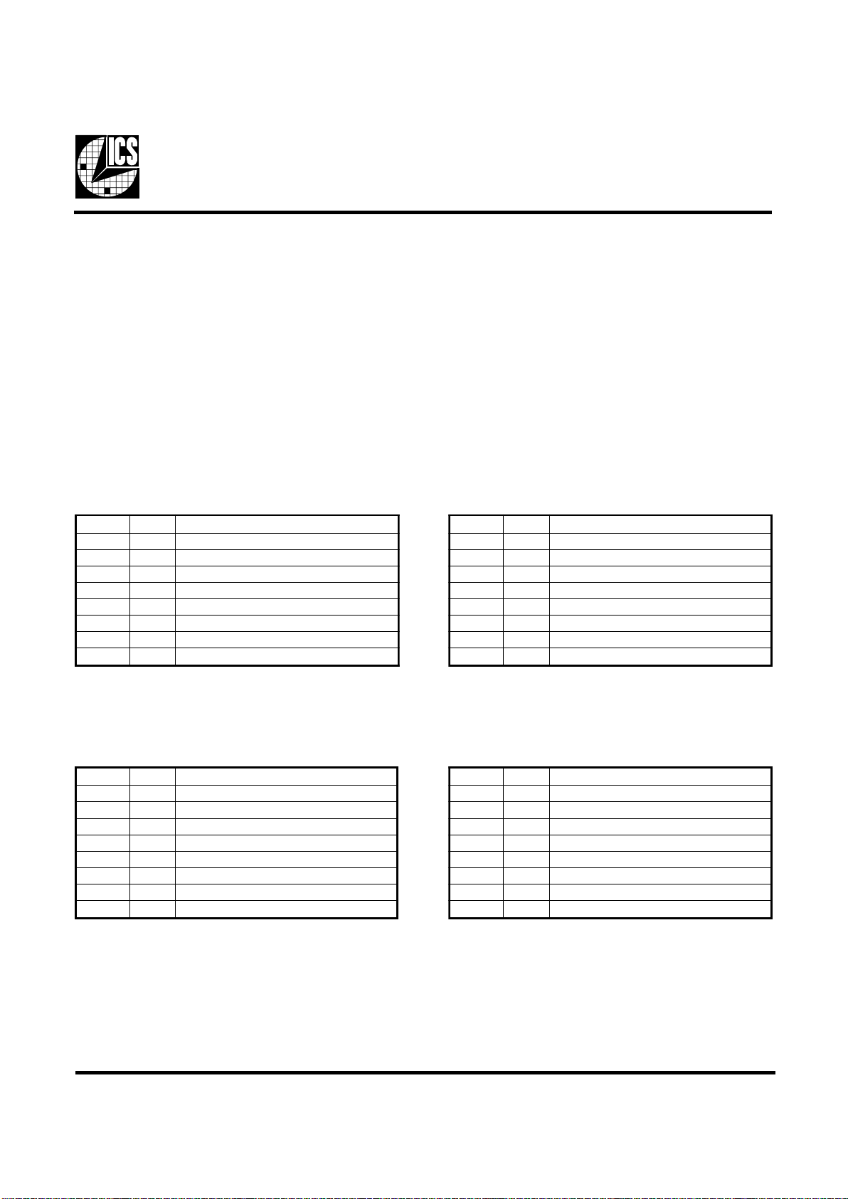
9
ICS94203
Note:
1. User needs to ensure step 3 & 7 is carried out. Systems with wrong spread percentage and/or group to group divider ratio
programmed into bytes 16-20 could be unstable. Step 3 & 7 assure the correct spread and gear ratio.
2. If VCO, REF divider values or phase detector stability are out of range, the device may fail to function correctly.
3. Follow min and max VCO frequency range provided. Internal PLL could be unstable if VCO frequency is too fast or too slow .
Use 14.31818MHz x VCO/REF divider values to calculate the VCO frequency (MHz).
4. Users can also utilize software utility provided to program VCO frequency from ICS Application Engineering.
5. Spread percent needs to be calculated based on VCO frequency , spread modulation frequency and spreadamount desired. See
Application note for software support.
Byte 16: Spread Sectrum Control Register
Byte 17: Spread Spectrum Control Register
Note: Please utilize software utility provided by ICS
Application Engineering to configure spread spectrum.
Incorrect spread percentage may cause system failure.
Note: Please utilize software utility provided by ICS
Application Engineering to configure spread spectrum.
Incorrect spread percentage may cause system failure.
Byte 18: Output Dividers Control Register
Byte 19: Output Dividers Control Register
Note: Changing bits in these registers results in frequency
divider ratio changes. Incorrect configuration of
group gear ratio can cause system malfunction.
Note: Changing bits in these registers results in frequency
divider ratio changes. Incorrect configuration of
group gear ratio can cause system malfunction.
Notes:
1. PWD = Power on Default
2. The power on default for byte 16-20 depends on the harware (latch inputs FS[0:4]) or IIC (Byte 0 bit [1:7]) setting. Be sure to read
back and re-write the values of these 5 registers when VCO frequency change is desired for the first pass.
tiBDWPnoitpircseD
7tiBX 7tiBlortnoCXUMrediviDtuptuO
6tiBX 6tiBlortnoCXUMrediviDtuptuO
5tiBX 5tiBlortnoCXUMrediviDtuptuO
4tiBX 4tiBlortnoCXUMrediviDtuptuO
3tiBX 3tiBlortnoCXUMrediviDtuptuO
2tiBX 2tiBlortnoCXUMrediviDtuptuO
1tiBX 1tiBlortnoCXUMrediviDtuptuO
0tiBX 0tiBlortnoCXUMrediviDtuptuO
tiBDWPnoitpircseD
7tiBX 51tiBlortnoCXUMrediviDtuptuO
6tiBX 41tiBlortnoCXUMrediviDtuptuO
5tiBX 31tiBlortnoCXUMrediviDtuptuO
4tiBX 21tiBlortnoCXUMrediviDtuptuO
3tiBX 11tiBlortnoCXUMrediviDtuptuO
2tiBX 01tiBlortnoCXUMrediviDtuptuO
1tiBX 9tiBlortnoCXUMrediviDtuptuO
0tiBX 8tiBlortnoCXUMrediviDtuptuO
tiBDWPnoitpircseD
7tiBX 7tiBmurtcepSdaerpS
6tiBX 6tiBmurtcepSdaerpS
5tiBX 5tiBmurtcepSdaerpS
4tiBX 4tiBmurtcepSdaerpS
3tiBX 3tiBmurtcepSdaerpS
2tiBX 2tiBmurtcepSdaerpS
1tiBX 1tiBmurtcepSdaerpS
0tiBX 0tiBmurtcepSdaerpS
tiBDWPnoitpircseD
7tiBX 62tiBlortnocrediviD
6tiB0 52tiBlortnocrediviD
5tiBX 42tiBlortnocrediviD
4tiBX 21tiBmurtcepSdaerpS
3tiBX 11tiBmurtcepSdaerpS
2tiBX 01tiBmurtcepSdaerpS
1tiBX 9tiBmurtcepSdaerpS
0tiBX 8tiBmurtcepSdaerpS
Page 10
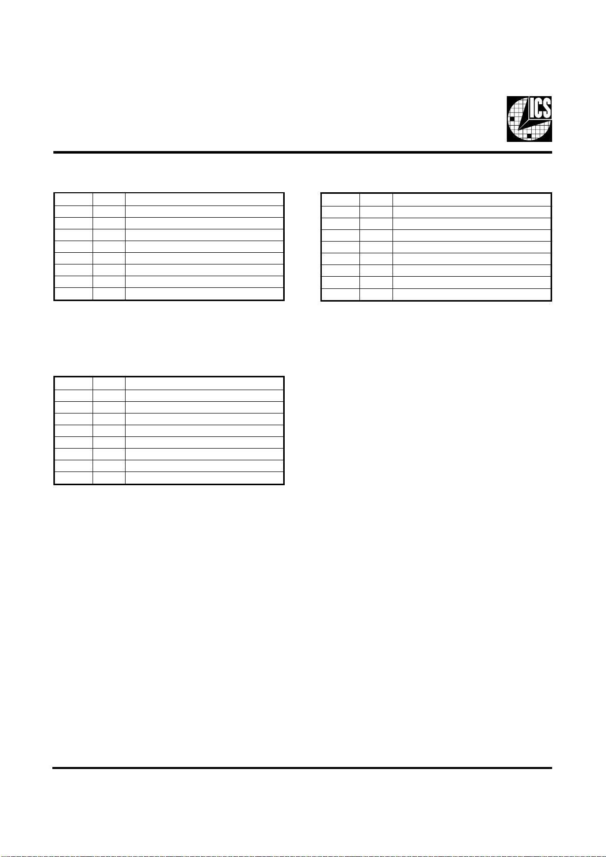
10
ICS94203
Byte 21: ICS Reserved Register
Notes:
1. PWD = Power on Default
Byte 22: Output Rise/Fall Time Select Register
Byte 20: Output Dividers Control Register
Note: Changing bits in these registers results in
frequency divider ratio changes. Incorrect
configuration of group gear ratio can cause
system malfunction.
Notes:
1. PWD = Power on Default
2. The power on default for byte 16-20 depends on the harware
(latch inputs FS[0:4]) or I
2
C (Byte 0 bit [1:7]) setting. Be sure
to read back and re-write the values of these 5 registers when
VCO frequency change is desired for the first pass.
3. If Byte 8 bit 7 is driven to "1" meaning programming is
intended, Byte 21-22 will lose their default power up value.
Note: Each increment or decrement of bit 4 to 7 will introduce
100ps delay or advance on all of the above clocks.
tiBDWPnoitpircseD
7tiBX 32tiBlortnoCXUMrediviDtuptuO
6tiBX 22tiBlortnoCXUMrediviDtuptuO
5tiBX 12tiBlortnoCXUMrediviDtuptuO
4tiBX 02tiBlortnoCXUMrediviDtuptuO
3tiBX 91tiBlortnoCXUMrediviDtuptuO
2tiBX 81tiBlortnoCXUMrediviDtuptuO
1tiBX 71tiBlortnoCXUMrediviDtuptuO
0tiBX 61tiBlortnoCXUMrediviDtuptuO
tiBDWPnoitpircseD
7tiB1 3tiBwekSICPot66V3
6tiB0 2tiBwekSICPot66V3
5tiB1 1tiBwekSICPot66V3
4tiB1 0tiBwekSICPot66V3
3tiB0 3tiBwekSCIPAOIot66V3
2tiB1 2tiBwekSCIPAOIot66V3
1tiB1 1tiBwekSCIPAOIot66V3
0tiB0 0tiBwekSCIPAOIot66V3
tiBDWPnoitpircseD
7tiB0 kaeW=1,lamroN=0zHM84,42
6tiB0 kaeW=1,lamroN=0FER/CIPAOI
5tiB0 kaeW=1,lamroN=0ICP
4tiB0 kaeW=1,lamroN=0F_MARDS
3tiB0 kaeW=1,lamroN=0]11:0[MARDS
2tiB0 kaeW=1,lamroN=066V3
1tiB0 kaeW=1,lamroN=01UPC
0tiB0 kaeW=1,lamroN=00UPC
Page 11
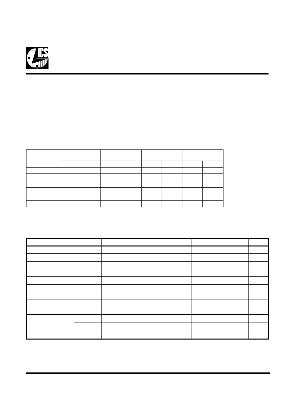
11
ICS94203
Absolute Maximum Ratings
Stresses above those listed under Absolute Maximum Ratings may cause permanent damage to the device. These ratings are stress
specifications only and functional operation of the device at these or any other conditions above those listed in the operational sections
of the specifications is not implied. Exposure to absolute maximum rating conditions for extended periods may affect product
reliability.
Core Supply Voltage . . . . . . . . . . . . . . . . . . . . . . . . 4.6 V
I/O Supply Voltage . . . . . . . . . . . . . . . . . . . . . . . . . 3.6V
Logic Inputs . . . . . . . . . . . . . . . . . . . . . . . . . . . . . . . GND –0.5 V to V
DD
+0.5 V
Ambient Operating Temperature . . . . . . . . . . . . . . 0°C to +70°C
Storage Temperature . . . . . . . . . . . . . . . . . . . . . . . . –65°C to +150°C
Case Temperature . . . . . . . . . . . . . . . . . . . . . . . . . . 115°C
Group Timing Relationship Table
1
puorGzHM66UPC
zHM001MARDS
zHM001UPC
zHM001MARDS
zHM331UPC
zHM001MARDS
zHM331UPC
zHM331MARDS
tesffOecnareloTtesffOecnareloTtesffOecnareloTtesffOecnareloT
MARDSotUPCsn5.2sp005sn0.5sp005sn0.0sp005sn57.3sp005
66V3otUPCsn5.7sp005sn0.5sp005sn0.0sp005sn0.0sp005
66V3otMARDSsn0.0sp005sn0.0sp005sn0.0sp005sn57.3sp005
ICPot66V3sn5.3-5.1sp005sn5.3-5.1sp005sn5.3-5.1sp005sn5.3-5.1sp005
ICPotICPsn0.0sn0.1sn0.0sn0.1sn0.0sn0.1sn0.0sn0.1
TOD&BSUhcnysAA/NhcnysAA/NhcnysAA/NhcnysAA/N
Electrical Characteristics - Input/Supply/Common Output Parameters
TA = 0 - 70º C; Supply Volt age VDD = 3.3 V +/-5% (unless otherwise stated)
PARAMETER SYMBOL CONDITIONS MIN TYP MAX UNITS
Input High Voltage V
IH
2V
DD
+0.3 V
Input Low Voltage V
IL
VSS-0.3 0.8 V
Input High Current I
IH
VIN = VDD 5 A
Input Low Current I
IL1
VIN=0 V;Inputs with no pull-up resistors -5 uA
Input Low Current I
IL2
VIN=0 V; Inputs with pull-up resistors -200 uA
Supply Current I
DD3.3OP100
CL=30 pF 346 400 mA
Power Down PD 4.3 600 mA
Input frequency Fi V
DD
= 3.3 V; 12 14.318 16 MHz
C
IN
Logic Inputs 5 pF
Input Capacitance1 C
IN
Logic Inputs 5 pF
C
INX
X1 & X2 pins 27 45 pF
Clk Stabilization
1
T
STAB
From VDD= 3.3 V to 1% target Freq.
3ms
1
Guaranteed by design, not 100% tested in production.
Page 12
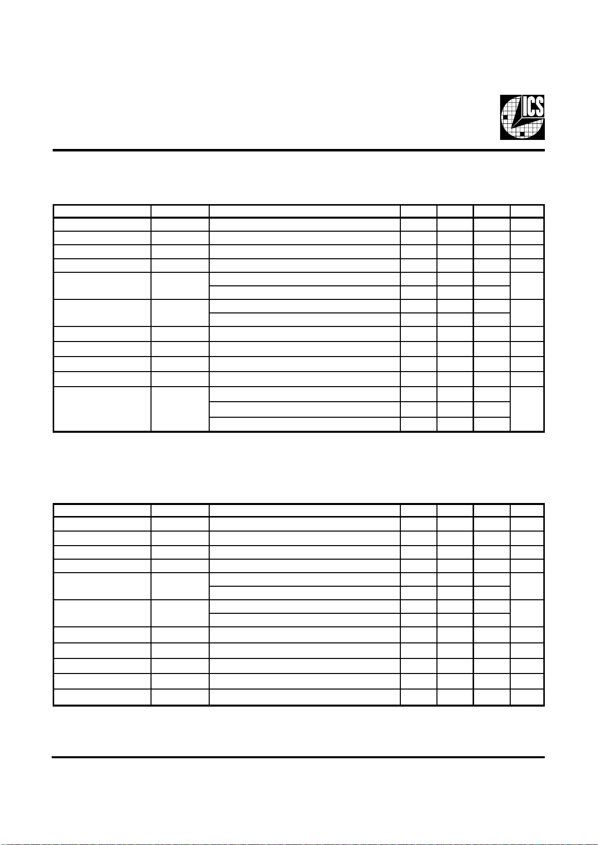
12
ICS94203
Electrical Characteristics - CPU
TA = 0 - 70C; V
DDL
= 2.5 V +/-5%; CL = 10-20 pF (unless otherwise specified)
PARAMETER SYMBOL CONDITIONS MIN TYP MAX UNITS
Out
p
ut Impedance
1
R
DSP2B
VO = VDD*(0.5)
13.5 20 45
Ω
Out
p
ut Impedance
1
R
DSN2B
VO = VDD*(0.5)
13.5 27 45
Ω
Output High Voltage
V
OH2B
IOH = -1 mA
22.5 V
Output Low Voltage
V
OL2B
IOL = 1 mA
0.18 0.4 V
V
OH @ MIN
= 1.0 V
-51 -27
V
OH @ MAX
= 2.375 V
-27 -11
V
OL @ MIN
= 1.2 V
27 41
V
OL @ MAX
= 0.3 V
15 30
Rise Time
1
t
r2B
VOL = 0.4 V, VOH = 2.0 V
0.4 1 1.6 ns
Fall Time
1
t
f2B
VOH = 2.0 V, VOL = 0.4 V
0.4 1 1.6 ns
Duty Cycle
1
d
t2B
VT = 1.25 V
45 49 55 %
Skew window
1
t
sk2B
VT = 1.25 V
40 175 ps
V
T
= 1.25 V, CPU=66 MHz
245 250
V
T
= 1.25 V, CPU=100 MHz
160 250
V
T
= 1.25 V, CPU=133 MHz
290 250
1
Guaranteed by design, not 100% tested in production.
ps
Jitter, Cycle-to-cycle
1
t
jcyc-cyc
mA
mA
Output High Current
Output Low Current
I
OH2B
I
OL2B
Electrical Characteristics - 3V66
TA = 0 - 70C; VDD = 3.3 V +/-5%; CL = 10-20 pF (unless otherwise specified)
PARAMETER SYMBOL CONDITIONS MIN TYP MAX UNITS
Output Impedance R
DSP1B
1
VO = VDD*(0.5) 12 17.4 55
Ω
Output Impedance R
DSN1B
1
VO = VDD*(0.5) 12 22.4 55
Ω
Output High Voltage V
OH1
IOH = -1 mA 2.4 3 .3 V
Output Low Voltage V
OL1
IOL = 1 mA 0.009 0.55 V
V
OH @ MIN
= 1.0 V -68 -29
V
OH @ MAX
= 3.135 V -27 -14
V
OL @ MIN
= 1.95 V 29 77
V
OL @ MAX
= 0.4 V 24 27
Rise Time
1
t
r1
VOL = 0.4 V, VOH = 2.4 V 0.5 1.4 2 ns
Fall Time
1
t
f1
VOH = 2.4 V, VOL = 0.4 V 0.5 1.7 2 ns
Duty Cycle
1
d
t1
VT = 1.5 V 45 49 55 %
Skew window
1
t
sk1
VT = 1.5 V 35 175 ps
Jitter, Cycle-to-cycle
1
t
jcyc-cyc1
VT = 1.5 V
292 500 ps
1
Guaranteed by design, not 100% tested in production.
Output High Current
Output Low Current
mA
mA
I
OH1
I
OL1
Page 13
13
ICS94203
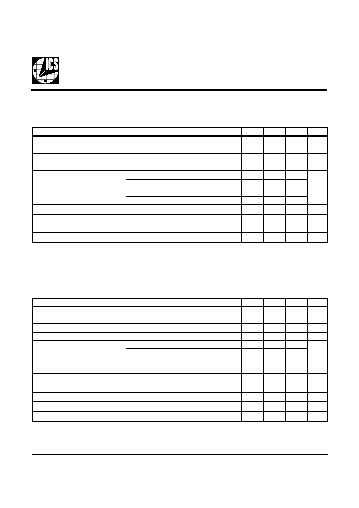
Electrical Characteristics - IOAPIC
TA = 0 - 70C; V
DDL
= 2.5 V +/-5%; CL = 10-20 pF (un le ss otherwise specif ied)
PARAMETER SYMBO
L
CONDITIONS MIN TYP MAX UNITS
Output Impedance R
DSP4B
1
VO = VDD*(0.5) 9 28 30 Ω
Output Impedance R
DSN4B
1
VO = VDD*(0.5) 9 28 30 Ω
Output High Voltage V
OH4B
IOH = -1 mA 2 2.4 V
Output Low Voltage V
OL4B
I
O
L
= 1 mA 0.25 0.4 V
V
OH @ MIN
= 1.0 V -62 -27
V
OH @ MAX
= 2.375 V -27 -12
V
OL @ MIN
= 1.2 V 27 35
V
OL @ MA
X
= 0.3 V 8 30
Rise Time
1
t
r4B
VOL = 0.4 V, VOH = 2.0 V 0.4 1.45 1.6 ns
Fall Time
1
t
f4B
VOH = 2.0 V, VOL = 0.4 V
0.40.971.6 ns
Duty Cycle
1
d
t4B
VT = 1.25 V 45 49.3 55 %
Jitter, Cycle-to-cycle
1
t
jcyc-cyc4B
VT = 1.25 V
130 500 ps
1
Guaranteed by design, not 100 % tested in production.
Output High Current
I
OH4B
mA
Output Low Current
I
OL4B
mA
Electrical Characteristi cs - SDRAM
TA = 0 - 70C; VDD = 3.3 V +/-5%; CL = 20-30 pF (unless otherwise specified)
PARAMETER SYMBOL CONDITIONS MIN TYP MAX UNITS
Output Impedance R
DSP3B
1
VO = VDD*(0.5) 10 16 24
Ω
Output Impedance R
DSN3B
1
VO = VDD*(0.5) 10 17.5 24
Ω
Output High Voltage V
OH3
IOH = -1 mA 2.4 3.3 V
Output Low Voltage V
OL3
IOL = 1 mA 0.01 0.4 V
V
OH @ MIN
= 2.0 V -70 -46
V
OH @ MAX
= 3.135 V -54 -29
V
OL @ MIN
= 1.0 V 54 90
V
OL @ MAX
= 0.4 V 28 53
Rise Time
1
t
r3
VOL = 0.4 V, VOH = 2.4 V 0.4 0.9 1.6 ns
Fall Time
1
t
f3
VOH = 2.4 V, VOL = 0.4 V 0.4 0.8 1.6 ns
Duty Cycle
1
d
t3
VT = 1.5 V 45 49.2 55 %
Skew window
1
t
sk3
VT = 1.5 V 83 250 ps
Jitter, Cycle-to-cycle
1
t
jcyc-cyc3
VT = 1.5 V, CPU=66,100,133 MHz
214 250
ps
1
Guaranteed by design, not 100% tested in production.
mA
mA
Output High Current
Output Low Current
I
OH3
I
OL3
Page 14
14
ICS94203
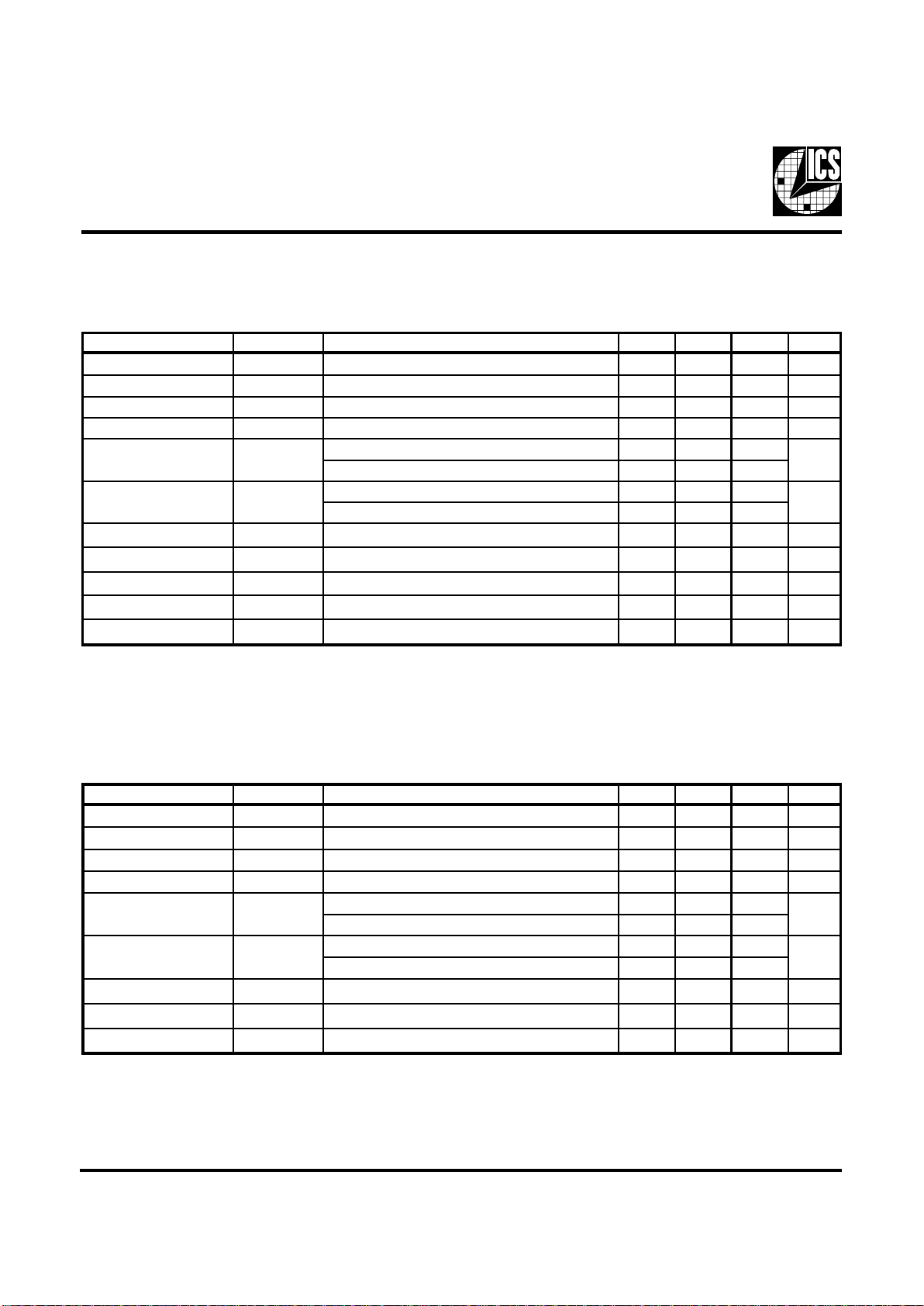
Electrical Characteristics - PCI
TA = 0 - 70C; VDD = 3.3 V +/-5%; CL = 10-30 pF (unless otherwise specified)
PARAMETER SYMBOL CONDITIONS MIN TYP MAX UNITS
Output Impedance R
DSP1B
1
VO = VDD*(0.5) 12 17.4 55
Ω
Output Impedance R
DSN1B
1
VO = VDD*(0.5) 12 22.4 55
Ω
Output High Voltage V
OH1
IOH = -1 mA 2.4 3 .3 V
Output Low Voltage V
OL1
IOL = 1 mA 0.009 0.55 V
V
OH @ MIN
= 1.0 V -67 -29
V
OH @ MAX
= 3.135 V -27 -14
V
OL @ MIN
= 1.95 V 29 77
V
OL @ MAX
= 0.4 V 24 27
Rise Time
1
t
r1
VOL = 0.4 V, VOH = 2.4 V 0.5 1.7 2.5 ns
Fall Time
1
t
f1
VOH = 2.4 V, VOL = 0.4 V 0.5 1.9 2.5 ns
Duty Cycle
1
d
t1
VT = 1.5 V 45 51 55 %
Skew window
1
t
sk1
VT = 1.5 V 213 500 ps
Jitter, Cycle-to-cycle
1
t
jcyc-cyc1
VT = 1.5 V
285 500 ps
1
Guaranteed by design, not 100% tested in production.
Output High Current
I
OH1
mA
Output Low Current
I
OL1
mA
Electrical Characteristics - REF, 48MHz
TA = 0 - 70C; VDD = 3.3 V +/-5%; CL = 10-20 pF (unless otherwise specified)
PARAMETER SYMBOL CONDITIONS MIN TYP MAX UNITS
Output Impedance R
DSP5B
1
VO = VDD*(0.5) 15 18 60 Ω
Output Impedance R
DSN5B
1
VO = VDD*(0.5) 15 18.75 60 Ω
Output High Voltage V
OH15
IOH = -1 mA 2.4 3.27 V
Output Low Voltage V
OL5
IOL = 1 mA 0.025 0.4 V
V
OH @ MI
N
= 1.0 V -76 -33
V
OH @ MAX
= 3.135 V -33 -12
V
OL @ MI
N
= 1.95 V 71 29
V
OL @ MAX
= 0.4 V 27 22
Rise Time
1
t
r5
V
O
L
= 0.4 V, VOH = 2.4 V 0.4 1 4 ns
Fall Time
1
t
f5
VOH = 2.4 V, V
O
L
= 0.4 V 0.4 1.7 4 ns
Duty Cycle
1
d
t5
VT = 1.5 V
45 54.1 55 %
1
Guaranteed by design, not 100% tested in production.
Output High Current
I
OH5
mA
Output Low Current
I
OL5
mA
Page 15
15
ICS94203
Fig. 1
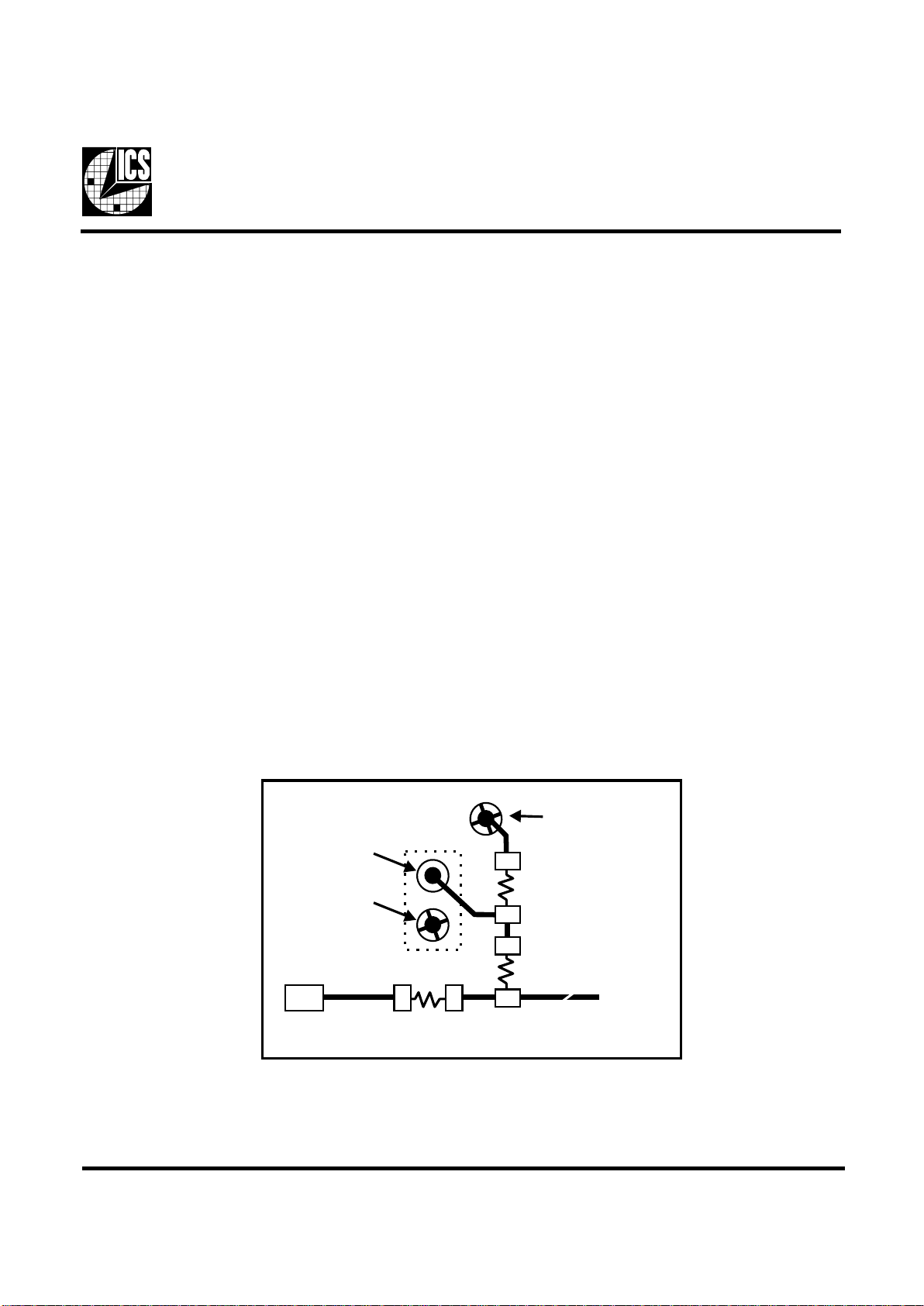
Shared Pin Operation Input/Output Pins
The I/O pins designated by (input/output) on the ICS94203
serve as dual signal functions to the device. During initial
power-up, they act as input pins. The logic level (voltage) that
is present on these pins at this time is read and stored into a 5bit internal data latch. At the end of Power -On reset, (see AC
characteristics for timing values), the device changes the
mode of operations for these pins to an output function. In this
mode the pins produce the specified buffered clocks to external
loads.
T o program (load) the internal configuration register for these
pins, a resistor is connected to either the VDD (logic 1) power
supply or the GND (logic 0) voltage potential. A 10 Kilohm
(10K) resistor is used to provide both the solid CMOS
programming voltage needed during the power-up
programming period and to provide an insignificant load on
the output clock during the subsequent operating period.
Via to
VDD
Clock trace to load
Series Term. Res.
Programming
Header
Via to Gnd
Device
Pad
2K
8.2K
Figure 1 shows a means of implementing this function when
a switch or 2 pin header is used. W ith no jumper is installed
the pin will be pulled high. W ith the jumper in place the pin
will be pulled low. If programmability is not necessary, than
only a single resistor is necessary . The programming resistors
should be located close to the series termination resistor to
minimize the current loop area. It is more important to locate
the series termination resistor close to the driver than the
programming resistor.
Page 16
16
ICS94203
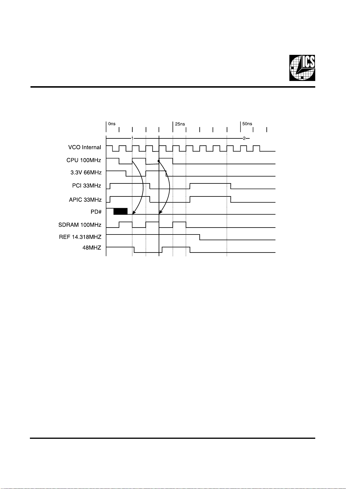
Power Down Waveform
Note
1. After PD# is sampled active (Low) for 2 consective rising edges of CPUCLKs, all the
output clocks are driven Low on their next High to Low tranistiion.
2. Power-up latency <3ms.
3. Waveform shown for 100MHz
Page 17
17
ICS94203
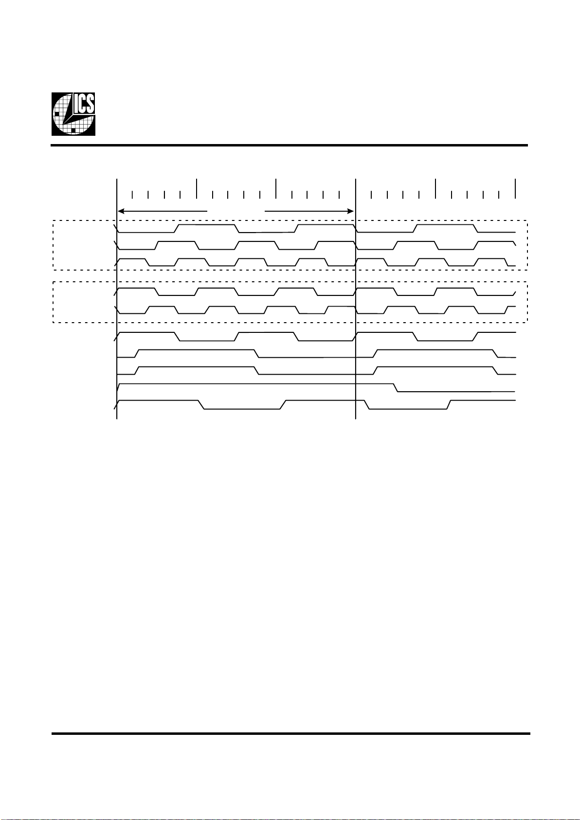
Group Offset Waveforms
Cycle Repeats
0ns
CPU 66MHz
CPU 100MHz
CPU 133MHz
SDRAM 133MHz
SDRAM 100MHz
3.5V 66MHz
PCI 33MHz
APIC 33MHz
REF 14.318MHz
USB 48MHz
10ns 20ns 30ns 40ns
Page 18
18
ICS94203
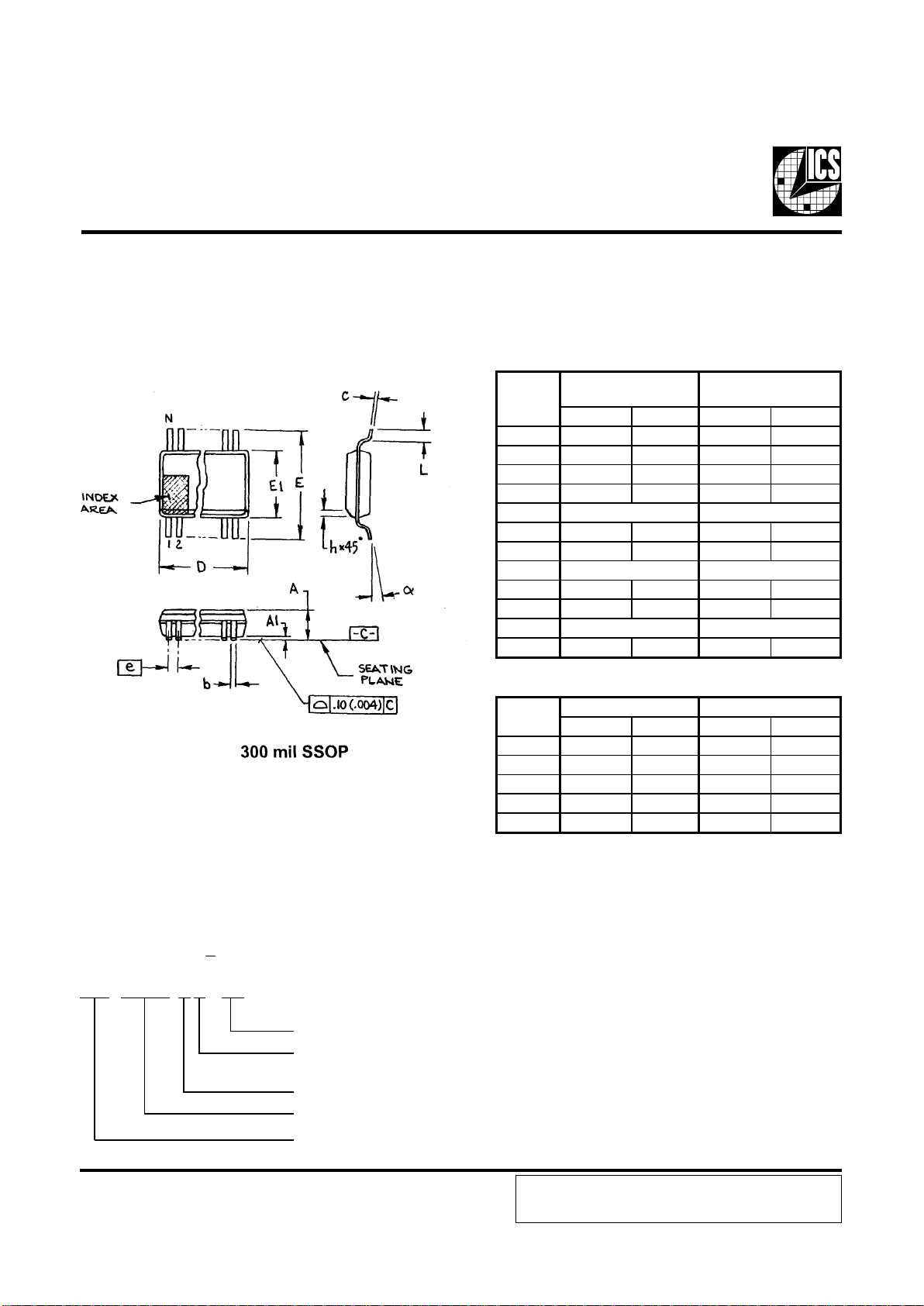
Ordering Information
ICS94203yF-T
Designation for tape and reel packaging
Package T ype
F=SSOP
Revision Designator (will not correlate with datasheet revision)
Device T ype
Prefix
ICS, AV = Standard Device
Example:
ICS XXXX y F - T
MIN MAX MIN MAX
A 2.413 2.794 .095 .110
A1 0.203 0.406 .008 .016
b 0.203 0.343 .008 .0135
c 0.127 0.254 .005 .010
D
E 10.033 10.668 .395 .420
E1 7.391 7.595 .291 .299
e 0.635 BASIC 0.025 BASIC
h 0.381 0.635 .015 .025
L 0.508 1.016 .020 .040
N
α
0° 8° 0° 8°
VARIATIONS
MIN MAX MIN MAX
28 9.398
9.652
.370 .380
34 11.303
11.557
.445 .455
48 15.748
16.002
.620 .630
56 18.288
18.542
.720 .730
64 20.828
21.082
.820 .830
SYMBOL
SEE VARIATIONS
SEE VARIATIONS
In Millimeters
COMMON DIMENSIONS
In Inches
COMMON DIMENSIONS
SEE VARIATION S
N
D mm.
D (inch)
SEE VARIATION S
ICS reserves the right to make changes in the device data identified in
this publication without further notice. ICS advises its customers to
obtain the latest version of all device data to verify that any
information being relied upon by the customer is current and accurate.
 Loading...