

Page 1
Integrated
Circuit
Systems, Inc.
General Description Features
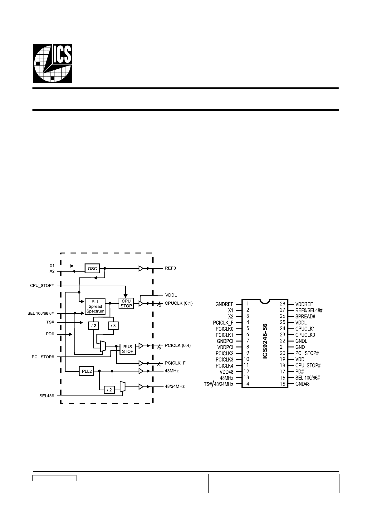
ICS9248-56
Block Diagram
Frequency Timing Generator for Pentium II Systems
9248-56 Rev E 12/27/00
Pin Configuration
28 pin SSOP and TSSOP
Pentium is a trademark on Intel Corporation.
• Generates the following system clocks:
- 2CPU(2.5V) up to 100MHz.
- 6 PCI(3.3V) @ 33.3MHz (Includes one free running).
- 1 REF clks (3.3V) at 14.318MHz.
- 1 Fixed clock at 48MHz
- 1 Fixed clock at 48 or 24MHz
• Skew characteristics:
- CPU – CPU
<175ps
- PCI – PCI < 500ps
- CPU(early) – PCI = 1.5ns – 4ns.
• Supports Spread Spectrum modulation for CPU and PCI
clocks, 0.5% down spread
• Efficient Power management scheme through stop clocks
and power down modes.
• Uses external 14.318MHz crystal, no external load cap
required for CL=18pF crystal.
• 28 pin 209mil SSOP and 173mil TSSOP
The ICS9248-56 is the Main clock solution for Notebook
designs using the Intel 440BX style chipset. Along with an
SDRAM buffer such as the ICS9179-03, it provides all
necessary clock signals for such a system.
Spread spectrum may be enabled by driving pin 26, SPREAD#
active (Low) at power-on. Spread spectrum typically reduces
system EMI by 8dB to 10dB. This simplifies EMI qualification
without resorting to board design iterations or costly shielding.
The ICS9248-56 employs a proprietary closed loop design,
which tightly controls the percentage of spreading over
process and temperature variations.
Power Groups
VDD, GND = PLL core
VDDREF , GNDREF = REF(0:1), X1, X2
VDDPCI, GNDPCI = PCICLK_F , PCICLK (0:4)
VDD48, GND48 = 48MHz, 48/24MHz
ICS reserves the right to make changes in the device data identified in
this publication without further notice. ICS advises its customers to
obtain the latest version of all device data to verify that any
information being relied upon by the customer is current and accurate.
Page 2
2
ICS9248-56
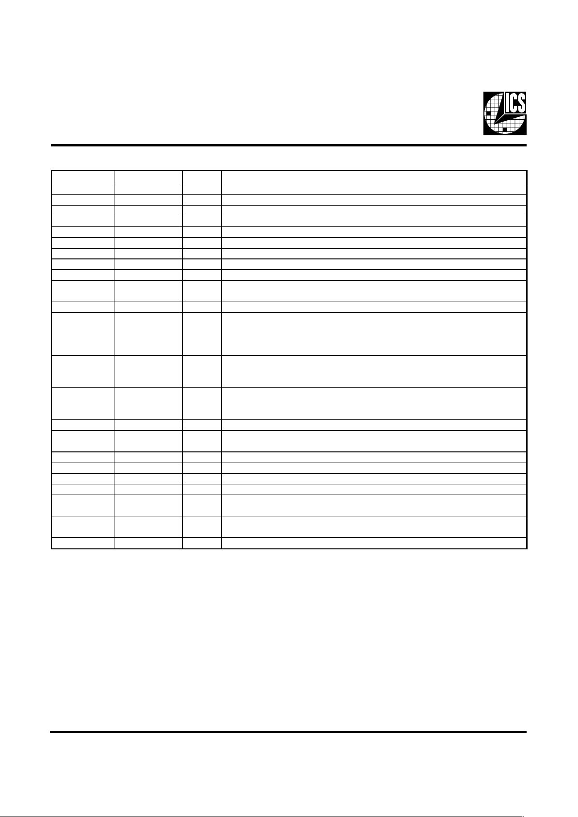
Pin Descriptions
Pin number Pin nam e Type Descript i on
1 GNDREF Power Ground for 14.318 MHz reference clock outputs
2 X1 Input 14.318 MHz crys tal input
3 X2 Output 14.318 MHz crystal output
4 PCICLK_F Output 3.3 V free running P CI clock output, wi l l not be stopped by the PCI_STOP#
5,6, 9,10,11 PCICLK (1: 5) Output 3.3 V P CI c l ock outputs, generat i ng timing requirem ents for Penti um II
7 GNDPCI Power Ground for PCI cloc k outputs
8 VDDPCI Power 3.3 V power for the PCI clock outputs
12 VDD48 Power 3.3 V power for 48/24 MHz c locks
13 48 MHz Output 3.3 V 48 MHz clock output, fixed frequenc y cloc k ty pi cally used with USB devices
14 TS#/48/24MHz Output
3.3 V 48 or 24 MHz output and Tri-st at e option, ac tive l ow = t ri state mode for test i ng,
act ive high = norm al operat ion
15 G ND48 Power Ground for 48/24 MHz clocks
16 SEL 100/66# Input
control for the frequency of clocks at the CPU & PCICLK output pins. If logic "0" is
used t he 66.6 MHz frequency i s selected. If Logic "1" is used, the 100 MHz
frequency i s selected. The PCI cl ock is multi pl exed to run at 33. 3 M Hz for bot h
selected cases.
17 PD# Input
As ynchronous active low input pin used t o power down t he device into a low power
state. The internal clocks are disabled and the VCO and the c ryst al are stopped. The
latency of the power down will not be greater than 3ms.
18 CPU_STOP# Input
As ynchronous active low input pin used to stop the CPUCLK in active low state, all
other clocks will continue to run. The CPUCLK will have a "Turnon " latency of at
leas t 3 CP U clock s.
19 VDD Power Isolated 3.3 V power for core
20 PCI-Stop# Input
Sy nchronous active low input used to stop the PCICLK i n active low state. It wil l not
effect P CICLK_F or any other outputs.
21 GND P ower Isolated ground for core
22 GNDL Power Ground for CPU clock out puts
23,24 CPUCLK(1:0) Output 2.5 V CPU clock out puts
25 VDDL Power 2.5 V power for CPU clock outputs
26 SPREAD# Output
Power-on spread s pectrum enable option. Active low = spread spectrum clocking
enable. Active high = spread spectrum clocking di sable.
27 REF0/SEL48# Ou tput
3.3 V 14. 318 M Hz referenc e clock output and power-on 48/24 MHz select option.
Ac tive low = 48 M Hz out put at pin 14. A ctive high = 24 MHz output at pi n 14.
28 V DDREF Power 3.3 V power for 14.318 MHz reference c l ock outputs.
Page 3
3
ICS9248-56
Select Functions
(Functionality determined by TS# and SEL100/66# pin, see below)
Notes:
1. TCLK is a test clock driven on the X1 (crystal in pin) input during test mode.
ytilanoitcnuFKLCUPC
,ICP
F_ICP
0FER
etatsirTZ-IHZ-IHZ-IH
edomtseT2/KLCT
1
6/KLCT
1
KLCT
1
#66/001LES#STnoitcnuF
00 etatS-irT
0- )devreseR(
0- )devreseR(
01 ICP3.33,UPCzHM6.66evitcA
10 edoMtseT
1- )devreseR(
1- )devreseR(
11 ICP3.33,UPCzHM001evitcA
Po wer Management
ICS9248-56 Power Management Requirements
Clock Enable Configuration
Full clock cycle timing is guaranteed at all times after the system has initially powered up except where noted. During power
up and power down operations using the PD# pin will not cause clocks of a short or longer pulse than that of the running clock.
The first clock pulse coming out of a stopped clock condition may be slightly distorted due to clock network charging circuitry .
Board routing and signal loading may have a large impact on the initial clock distortion also.
Notes.
1. Clock on latency is defined from when the clock enable goes active to when the first valid clock comes out of the device.
2. Clock off latency is defined from when the clock enable goes inactive to when the last clock is driven low out of the device.
3. Power up latency is when PD# goes inactive (high) to when the first valid clocks are output by the device.
4. Power down has controlled clock counts applicable to CPUCLK, PCICLK only.
The REF will be stopped independant of these.
LANGISETATSLANGIS
ycnetaL
gninnureerffosegdegnisirfo.oN
KLCICP
#POTS_UPC)delbasiD(0
2
1
)delbanE(1
1
1
#POTS_ICP)delbasiD(0
2
1
)delbanE(1
1
1
#DP)noitarepOlamroN(1
3
sm3
)nwoDrewoP(0
4
xam2
#POTS_UPC#POTS_ICP#NWD_RWPKLCUPCKLCICPF_KLCICPFERlatsyrCsOCV
XX 0 woLwoLwoLdeppotSffOffO
00 1 woLwoLzHM3.33gninnuRgninnuRgninnuR
011 woLzHM3.33zHM3.33gninnuRgninnuRgninnuR
10 1 zHM6.66/001woLzHM3.33gninnuRgninnuRgninnuR
11 1 zHM6.66/001zHM3.33zHM3.33gninnuRgninnuRgninnuR
Page 4
4
ICS9248-56
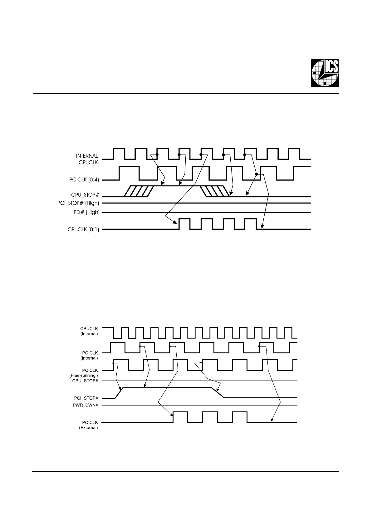
PCI_STOP# Timing Diagram
PCI_STOP# is an asynchronous input to the ICS9248-56. It is used to turn off the PCICLK (0:4) clocks for low power operation.
PCI_STOP# is synchronized by the ICS9248-56 internally . The minimum that the PCICLK (0:4) clocks are enabled (PCI_STOP#
high pulse) is at least 10 PCICLK (0:4) clocks. PCICLK (0:4) clocks are stopped in a low state and started with a full high pulse
width guaranteed. PCICLK (0:4) clock on latency cycles are only one rising PCICLK clock off latency is one PCICLK clock.
CPU_STOP# Timing Diagram
CPUSTOP# is an asychronous input to the clock synthesizer. It is used to turn off the CPUCLKs for low power operation.
CPU_STOP# is synchronized by the ICS9248-56. The minimum that the CPUCLK is enabled (CPU_STOP# high pulse) is 100
CPUCLKs. All other clocks will continue to run while the CPUCLKs are disabled. The CPUCLKs will always be stopped in a low
state and start in such a manner that guarantees the high pulse width is a full pulse. CPUCLK on latency is less than 4 CPUCLKs
and CPUCLK off latency is less than 4 CPUCLKs.
Notes:
1. All timing is referenced to the internal CPUCLK.
2. CPU_STOP# is an asynchronous input and metastable conditions may exist.
This signal is synchronized to the CPUCLKs inside the ICS9248-56.
3. All other clocks continue to run undisturbed.
4. PD# and PCI_STOP# are shown in a high (true) state.
Notes:
1. All timing is referenced to the Internal CPUCLK (defined as inside the ICS9248 device.)
2. PCI_STOP# is an asynchronous input, and metastable conditions may exist. This signal is required to be synchronized
inside the ICS9248.
3. All other clocks continue to run undisturbed.
4. PD# and CPU_STOP# are shown in a high (true) state.
Page 5

5
ICS9248-56
PD# Timing Diagram
The power down selection is used to put the part into a very low power state without turning off the power to the part. PD# is
an asynchronous active low input. This signal is synchronized internally by the ICS9248-56 prior to its control action of
powering down the clock synthesizer. Internal clocks will not be running after the device is put in power down state. When PD#
is active (low) all clocks are driven to a low state and held prior to turning off the VCOs and the crystal oscillator . The power on
latency is guaranteed to be less than 3 ms. The power down latency is less than three CPUCLK cycles. PCI_STOP# and
CPU_STOP# are don’t care signals during the power down operations.
Notes:
1. All timing is referenced to the Internal CPUCLK (defined as inside the ICS9248 device).
2. PD# is an asynchronous input and metastable conditions may exist. This signal is synchronized inside the ICS9248.
3. The shaded sections on the VCO and the Crystal signals indicate an active clock is being generated.
Page 6

6
ICS9248-56
Absolute Maximum Ratings
Supply Voltage. . . . . . . . . . . . . . . . . . . . . . . . . . . 7.0 V
Logic Inputs . . . . . . . . . . . . . . . . . . . . . . . . . . . . GND –0.5 V to VDD +0.5 V
Ambient Operating Temperature . . . . . . . . . . . . 0°C to +70°C
Storage Temperature . . . . . . . . . . . . . . . . . . . . . . –65°C to +150°C
Stresses above those listed under Absolute Maximum Ratings may cause permanent damage to the device. These ratings are
stress specifications only and functional operation of the device at these or any other conditions above those listed in the
operational sections of the specifications is not implied. Exposure to absolute maximum rating conditions for extended periods
may affect product reliability .
Electrical Characteristics - Input/Supply/Common Output Parameters
TA = 0 - 70C; Supply Voltage VDD = V
DDL
= 3.3 V +/-5% (unless otherwise state
d)
PARAMETER
S
YMBOL
CO
NDITION
S
MIN TYP MAX UNIT
S
Input High Voltage V
IH
2V
DD
+0.3 V
Input Low Voltage V
IL
VSS-0.3 0.8 V
Input High Current I
IH
VIN = V
DD
0.1 5
µ
A
Input Low Current I
IL1
VIN = 0 V; Inputs with no pull-up resistors -5 2.0
µ
A
Input Low Current I
IL2
VIN = 0 V; Inputs with pull-up resistors -200 -100
µ
A
Operating I
DD3.3OP66CL
= 0 pF; Select @ 66MHz 60 180 mA
Supply Current I
DD3.3OP100CL
= 0 pF; Select @ 100MHz 66 180 mA
Power Down I
DD3.3PD
CL = 0 pF; With input address to Vdd or GND 70 600
µ
A
Supply Current
Input frequency F
i
VDD = 3.3 V; 11 14.318 16 MHz
Input Capacitance
1
C
IN
Logic Inputs 5 pF
C
INX
X1 & X2 pins 27 36 45 pF
Transition Time
1
T
trans
To 1st crossing of target Freq. 3 ms
Clk Stabilization
1
T
STAB
From VDD = 3.3 V to 1% target Freq. 3 ms
Sk
ew
1
T
CPU-PCI
VT = 1.5 V;
1.5 2.4 4 ns
1
Guaranteed by design, not 100% tested in production.
Electrical Characteristics - Input/Supply/Common Output Parameters
TA = 0 - 70C; Supply Voltage VDD = 3.3 V +/-5%, V
DDL
= 2.5 V +/-5% (unless otherwise stated)
PARAMETER SYMBOL CONDITIONS MIN TYP MAX UNITS
Operating I
DD2.5OP66CL
= 0 pF; Select @ 66.8 MHz 16 72 mA
Supply Current I
DD2.5OP100CL
= 0 pF; Select @ 100 MHz 23 100 mA
Skew
1
t
CPU-PCI2
VT = 1.5 V; VTL = 1.25 V
1.5 3 4 ns
1
Guaranteed by design, not 100% tested in prod uction.
Page 7

7
ICS9248-56
Electrical Characteristics - CPUCLK
TA = 0 - 70C; VDD = 3.3 V +/-5%, V
DDL
= 2.5 V +/-5%;
C
L
= 10 - 20 pF (unless otherwise state
d)
PARAMETER
S
YMBOL
CO
NDITION
S
MIN TYP MAX UNIT
S
Output High Voltage V
OH2B
IOH = -12.0 mA 1.8 2.3 V
Output Low Voltage V
OL2B
IOL = 12 mA 0.31 0.4 V
Output High Current I
OH2B
VOH = 1.7 V -27 mA
Output Low Current I
OL2B
VOL = 0.7 V 27 mA
Rise Time t
r2B
1
VOL = 0.4 V, VOH = 2.0 V 0.4 1.15 1.6 ns
Fall Time t
f2B
1
VOH = 2.0 V, VOL = 0.4 V 0.4 1.4 1.6 ns
Duty Cycle d
t2B
1
VT = 1.25 V 44 48 55 %
Skew t
sk2B
1
VT = 1.25 V 134 175 ps
t
jcyc-cyc2B
1
VT = 1.25 V 186 250 ps
t
j1s2B
1
VT = 1.25 V 52 150 ps
t
jabs2B
1
VT = 1.25 V
-250 150 +250 ps
1
Guaranteed by design, not 100% tested in production.
Jitter
Electrical Characteristics - PCICLK
TA = 0 - 70C; VDD = V
DDL
= 3.3 V +/-5%; CL = 30 pF
PARAMETER SYMBOL CONDITIONS MIN TYP MAX UNITS
Output High Voltage V
OH1
IOH = -18 mA 2.1 3.3 V
Output Low Voltage V
OL1
IOL = 9.4 mA 0.1 0.4 V
Output High Current I
OH1
VOH = 2.0 V -22 mA
Output Low Current I
OL1
VOL = 0.8 V 16 57 mA
Rise Time
1
t
r1
VOL = 0.4 V, VOH = 2.4 V 1.6 2 ns
Fall Time
1
t
f1
VOH = 2.4 V, VOL = 0.4 V 1.8 2 ns
Duty Cycle
1
d
t1
VT = 1.5 V 45 50 55 %
Skew
1
t
sk1
VT = 1.5 V 222 500 ps
t
jcyc-cyc
1
VT = 1.5 V 186 500 ps
t
j
1s1
VT = 1.5 V 52 150 ps
t
jabs1
VT = 1.5 V
200 500 ps
1
Guaranteed by design, not 100 % te sted in production.
Jitter
Page 8

8
ICS9248-56
Electrical Characteristics - REF/48MHz/24MHz
TA = 0 - 70C; VDD = V
DDL
= 3.3 V +/-5%; CL = 10 - 20 pF (unless otherwise stated)
PARAMETER SYMBOL CONDITIONS MIN TYP MAX UNITS
Output High Voltage V
OH5
IOH = -12 mA 2.6 3.1 V
Output Low Voltage V
OL5
IOL = 9 mA 0.17 0.4 V
Output High Current I
OH5
VOH = 2.0 V -44 -22 mA
Output Low Current I
OL5
VOL = 0.8 V 16 42 mA
Rise Time
1
t
r5
VOL = 0.4 V, VOH = 2.4 V 1.4 4 ns
Fall Time
1
t
f5
VOH = 2.4 V, VOL = 0.4 V 1.1 4 ns
Duty Cycle
1
d
t5
VT = 1.5 V 45 53 55 %
t
j1σ
5
VT = 1.5 V, REF 185 250 ps
t
j
abs5
VT = 1.5 V, REF 385 800 ps
t
j1σ
5
VT = 1.5 V, 48 MHz 169 250 ps
t
jabs5
VT = 1.5 V, 48 MHz
469 800 ps
Jitter
1
Jitter
1
Page 9

9
ICS9248-56
General Layout Precautions:
1) Use a ground plane on the top layer of the
PCB in all areas not used by traces.
2) Make all power traces and vias as wide as
possible to lower inductance.
Notes:
1 All clock outputs should have series
terminating resistor. Not shown in all
places to improve readibility of
diagram
2 Optional EMI capacitor should be
used on all CPU, SDRAM, and PCI
outputs.
3 Optional crystal load capacitors are
recommended.
Capacitor V alues:
C1, C2 : Crystal load values determined by user
All unmarked capacitors are 0.01F ceramic
Page 10

10
ICS9248-56
Ordering Information
ICS9248F-56
Pattern Number (2 or 3 digit number for parts with ROM code patterns)
Package Type
F=SSOP
Revision Designator
Device Type (consists of 3 or 4 digit numbers)
Prefix
ICS, AV = S tandard Device
Example:
ICS XXXXy F - PPP
MIN MAX MIN MAX
A - 2.00 - .079
A1 0.05 - .002 A2 1.65 1.85 .065 .073
b 0.22 0.38 .009 .015
c 0.09 0.25 .0035 .010
D
E 7.40 8.20 .291 .323
E1 5.00 5.60 .197 .220
e
L 0.55 0.95 .022 .037
N
α
0° 8° 0° 8°
VARIATIONS
MIN MAX MIN MAX
28 9.90
10.50
.390 .413
MO-150 JEDEC
Doc.# 10-0033
6/1/00 Rev B
N
D mm.
D (inch)
SEE VARIATIONS
SYMBOL
SEE VARIATIONS
SEE VARIATIONS
In Millimeters
COMMON DIMENSIONS
In Inches
COMMON DIMENSIONS
SEE VARIATIONS
0.65 BASIC 0.0256 BASI C
ICS reserves the right to make changes in the device data identified in
this publication without further notice. ICS advises its customers to
obtain the latest version of all device data to verify that any
information being relied upon by the customer is current and accurate.
Page 11

11
ICS9248-56
Ordering Information
ICS9248yG-56-T
Designation for tape and reel packaging
Pattern Number (2 or 3 digit number for parts with ROM code patterns)
Package Type
G=TSSOP
Revision Designator (will not correlate with datasheet revision)
Device Type (consists of 3 or 4 digit numbers)
Prefix
ICS, AV = S tandard Device
Example:
ICS XXXX y G - PPP - T
4.40 mm. Body , 0.65 mm. pitch TSSOP
(173 mil)
(0.0256 mil)
MIN MAX MIN MAX
A - 1.20 - .047
A1 0.05 0.15 .002 .006
A2 0.80 1.05 .032 .041
b 0.19 0.30 .007 .012
c 0 .09 0.20 .003 5 .008
D
E
E1 4.30 4.50 .169 .177
e 0.65 BASIC 0.0256 BASIC
L 0.45 0.75 .018 .030
N
α
0° 8° 0° 8°
aaa - 0.10 - .004
VARIATI ONS
MIN MAX MIN MAX
28 9.60
9.80
.378 .386
MO-153 JEDEC
Doc. # 10-0038
7/6/ 00 Rev B
SY MBOL
SEE VARIATIONS
SEE VARIATIONS
In Millimet ers
COMMON DIMENSIONS
In Inc hes
COMMON DIMENSIONS
SEE VARIATIONS
6.40 BASIC 0.25 2 BASIC
N
D mm.
D (inch)
SEE VARIATIONS
ICS reserves the right to make changes in the device data identified in
this publication without further notice. ICS advises its customers to
obtain the latest version of all device data to verify that any
information being relied upon by the customer is current and accurate.
 Loading...