

Page 1
Integrated
Circuit
Systems, Inc.
ICS9248-87
Third party brands and names are the property of their respective owners.
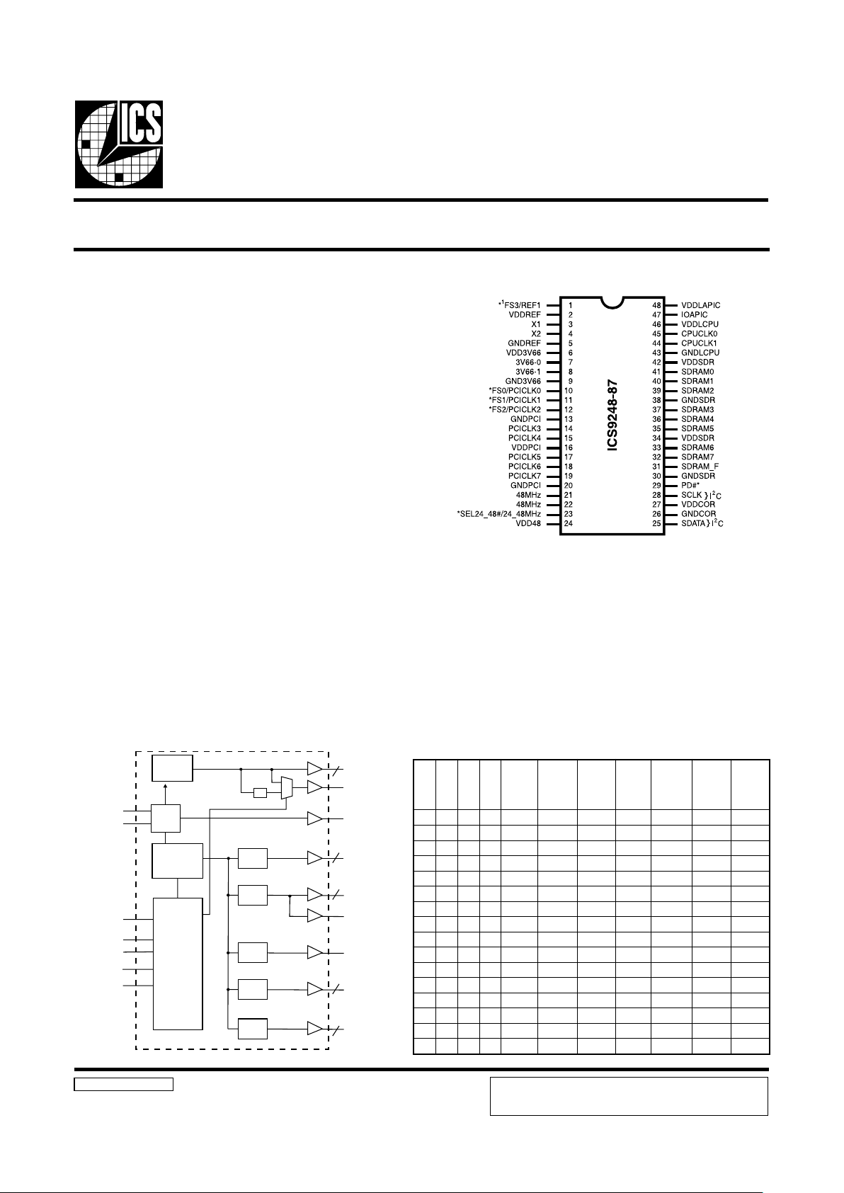
Block Diagram
9248-87 Rev D 10/27/00
Recommended Application:
810/810E type chipset.
Output Features:
• 2- CPUs @2.5V, up to 155MHz.
• 9 - SDRAM @ 3.3V, up to 155MHz.
• 8 - PCICLK @ 3.3V
• 1 - IOAPIC @ 2.5V,
• 2 - 3V66MHz @ 3.3V
• 2- 48MHz, @3.3V fixed.
• 1- 24/48MHz, @3.3V
• 1- REF @3.3V, 14.318MHz.
Features:
• Up to 155MHz frequency support
• Support FS0-FS3 strapping status bit for I
2
C read back.
• Support power management: Power down Mode from I
2
C
programming.
• Spread spectrum for EMI control ( ± 0.25% center).
• Uses external 14.318MHz crystal
Skew Specifications:
• CPU – CPU: <175ps
• SDRAM - SDRAM: < 250ps
• 3V66 – 3V66: <175ps
• PCI – PCI: <500ps
• For group skew specification, please refer to group
timing relationships table.
Preliminary Product Preview
Functionality
Pin Configuration
48-Pin 300mil SSOP
*: These inputs have a 120K pull up to VDD.
1: These are double strength.
3SF2SF1SF0SF
UPC
)zHM(
/UPC
MARDS
MARDS
)zHM(
66V3
)zHM(
KLCICP
*66V3(
)2/1
)zHM(
CIPAOI
*ICP(
)2/1
)zHM(
CIPAOI
)ICP(
)zHM(
0000
3.3800.13.3884.5547.7278.3147.72
0001
00.42100.100.42176.2833.1476.0233.14
0010
00.55100.100.55133.30176.1538.5276.15
0011
69.34133.100.80100.2700.6300.8100.63
0100
00.0776.000.50100.0700.5305.7100.53
0101
00.21100.100.21176.4733.7376.8133.73
0110
00.05100.100.05100.00100.0500.5200.05
0111
00.04133.100.50100.0700.5305.7100.53
1000
33.8676.005.20133.8671.4380.7171.43
1001
00.70100.100.70133.1776.5338.7176.53
10 10
00.83100.100.83100.2900.6400.3200.64
10 11
33.73133.100.30176.8643.4371.7143.43
1100
08.6676.002.00108.6604.3307.6104.33
1101
03.00100.103.00108.6604.3307.6104.33
1110
06.33100.106.33170.9835.4472.2235.44
1111
06.33133.102.00108.6604.3307.6104.33
Frequency Generator & Integrated Buffers for Celeron & PII/III™
SEL24_48#
PLL2
PLL1
Spread
Spectrum
48MHz
24_48MHz
CPUCLK [1:0]
SDRAM [7:0]
SDRAM_F
IOAPIC
PCICLK [7:0]
8
2
8
2
2
3V66 [1:0]
X1
X2
XTAL
OSC
CPU
DIVDER
SDRAM
DIVDER
IOAPIC
DIVDER
PCI
DIVDER
3V66
DIVDER
S DATA
SCLK
IC
2
FS[3:0]
PD#
Control
Logic
Config.
Reg.
/ 2
REF1
{
PRODUCT PREVIEW documents contain information on new
products in the sampling or preproduction phase of development.
Characteristic data and other specifications are subject to change
without notice.
Page 2
2
ICS9248-87
Preliminary Product Preview
Third party brands and names are the property of their respective owners.
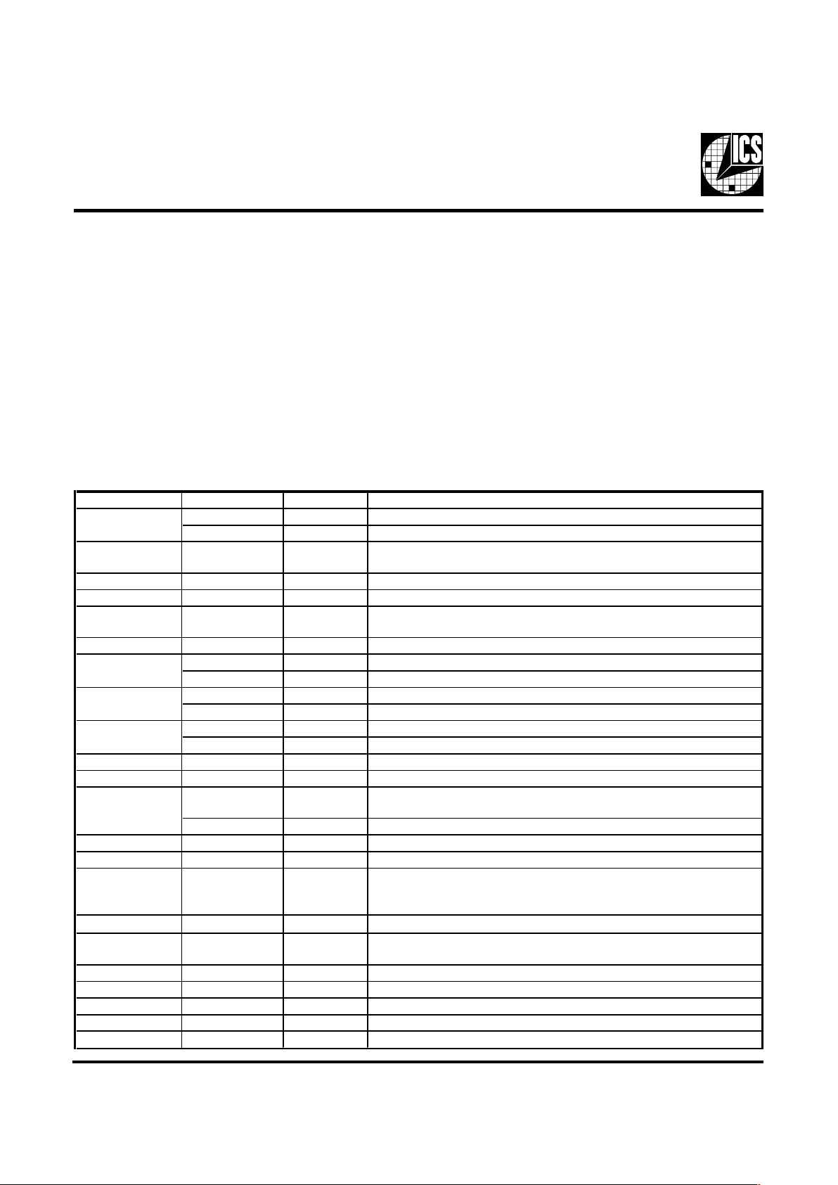
General Description
Pin Configuration
Power Groups
GNDREF, VDDREF = REF1, X1, X2
GNDPCI, VDDPCI = PCICLK [7:0]
GNDSDRAM, VDDSDRAM = SDRAM [8:0]
GND3V66, VDD3V66 = 3V66
VDD48 = 48MHz, 24MHz
GNDCOR, VDDCOR = supply for PLL core
VDDLAPIC = IOAPIC
GNDLCPU, VDDLCPU = CPUCLKL [1:0]
The ICS9248-87 is the single chip clock solution for designs
using 810/810E style chipset. It provides all necessary clock
signals for such a system.
Spread spectrum may be enabled through I
2
C programming.
Spread spectrum typically reduces system EMI by 8dB to
10dB. This simplifies EMI qualification without resorting to
board design iterations or costly shielding. The ICS9248-87
employs a proprietary closed loop design, which tightly
controls the percentage of spreading over process and
temperature variations.
Serial programming I
2
C interface allows changing functions,
stop clock programming and frequency selection.
PIN NUMBER PIN NAME TYPE DESCRIPTION
REF1 OUT 14.318 MHz reference clock.
FS3 IN Frequency select pin.
2, 6, 16, 24, 27, 34,
42
VDD PWR
3.3V Power supply for SD R A M output buffers, PCI output buff ers , re ference
o
utput buffers and 48MHz output
3 X1 IN Crystal input,no mi nally 14.318MHz.
4 X2 OUT Crystal output, nominally 14.318MHz.
5, 9, 13, 20, 26, 30,
38
GND PWR Ground pin for 3V outputs.
8, 7 3V66 [1:0] OUT 3V66 clock outputs.
FS0 IN Frequency select pin.
PCICLK0 OUT PCI clock outp ut .
FS1 IN Frequency select pin.
PCICLK1 OUT PCI clock outp ut .
FS2 IN Frequency select pin.
PCICLK2 OUT PCI clock outp ut .
19, 18, 17, 15, 14 PCICLK [7:3] OUT PCI clock outputs.
21, 22 48MHz OUT 48MHz output clocks
SEL24_48# IN
Sel pin for enabling 24MHz or 48MHz
H=24MHz L=48MHz
24_48MHz OUT Clock output for super I/O/USB
25 SDATA IN Data input for I2C serial input, 5V tolera nt input
28 SCLK IN Clock input of I2C input, 5V t ole rant input
29 PD# IN
Asynchronous active low input pin used to power down the devic e into a low
power state. The internal clocks are disabled and the VCO and the crystal are
s
topped. The latency of the power down will not be greater than 3ms.
31 SDRAM_F OUT
SDRAM clock output - free running not affected by I
2
C
32, 33, 35, 36, 37,
39, 40, 41
SDRAM [7:0] OUT SDRAM clock outputs
43 GNDL C P U PWR Ground pin for the CPU clocks.
44, 45 CPUCLK [1:0] OUT CPU clock output s.
46 VDDLCPU PWR Power pin for the CPUCLKs. 2.5V
47 IOAPIC OUT 2.5V clock output
48 VDDLAPIC PWR Power pin f or the IOAPIC. 2.5V
23
1
11
12
10
Page 3
3
ICS92 48-87
Preliminary Product Preview
Third party brands and names are the property of their respective owners.
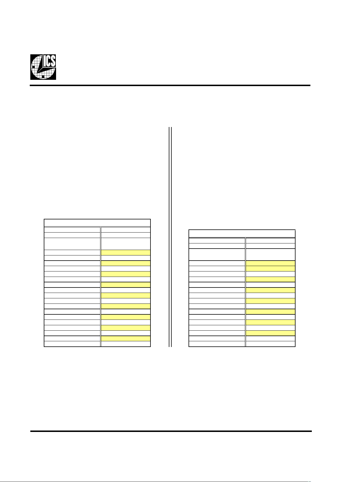
1. The ICS clock generator is a slave/receiver, I2C component. It can read back the data stored in the latches for
verification. Read-Back will support Intel PIIX4 "Block-Read" protocol.
2. The data transfer rate supported by this clock generator is 100K bits/sec or less (standard mode)
3. The input is operating at 3.3V logic levels.
4. The data byte format is 8 bit bytes.
5. To simplify the clock generator I
2
C interface, the protocol is set to use only "Block-Writes" from the controller. The
bytes must be accessed in sequential order from lowest to highest byte with the ability to stop after any complete byte
has been transferred. The Command code and Byte count shown above must be sent, but the data is ignored for those
two bytes. The data is loaded until a Stop sequence is issued.
6. At power-on, all registers are set to a default condition, as shown.
General I2C serial interface information
The information in this section assumes familiarity with I2C programming.
For more information, contact ICS for an I
2
C programming application note.
How to Write:
Controller (host) sends a start bit.
Controller (host) sends the write address D2
(H)
ICS clock will acknowledge
Controller (host) sends a dummy command code
ICS clock will acknowledge
Controller (host) sends a dummy byte count
ICS clock will acknowledge
Controller (host) starts sending first byte (Byte 0)
through byte 5
ICS clock will acknowledge each byte one at a time.
Controller (host) sends a Stop bit
How to Read:
Controller (host) will send start bit.
Controller (host) sends the read address D3
(H)
ICS clock will acknowledge
ICS clock will send the byte count
Controller (host) acknowledges
ICS clock sends first byte (Byte 0) through byte 5
Controller (host) will need to acknowledge each byte
Controller (host) will send a stop bit
Notes:
Controller (Host) ICS (Slave/Receiver)
Start Bit
Address
D3
(H)
ACK
Byte Count
ACK
Byte 0
ACK
Byte 1
ACK
Byte 2
ACK
Byte 3
ACK
Byte 4
ACK
Byte 5
ACK
Stop Bit
H
ow to Read:
Controller (Host) ICS (Slave/Receiver)
Start Bit
Address
D2
(H)
ACK
Dummy Command Code
ACK
Dummy Byte Count
ACK
Byte 0
ACK
Byte 1
ACK
Byte 2
ACK
Byte 3
ACK
Byte 4
ACK
Byte 5
ACK
Stop Bit
H
ow to Write:
Page 4
4
ICS9248-87
Preliminary Product Preview
Third party brands and names are the property of their respective owners.
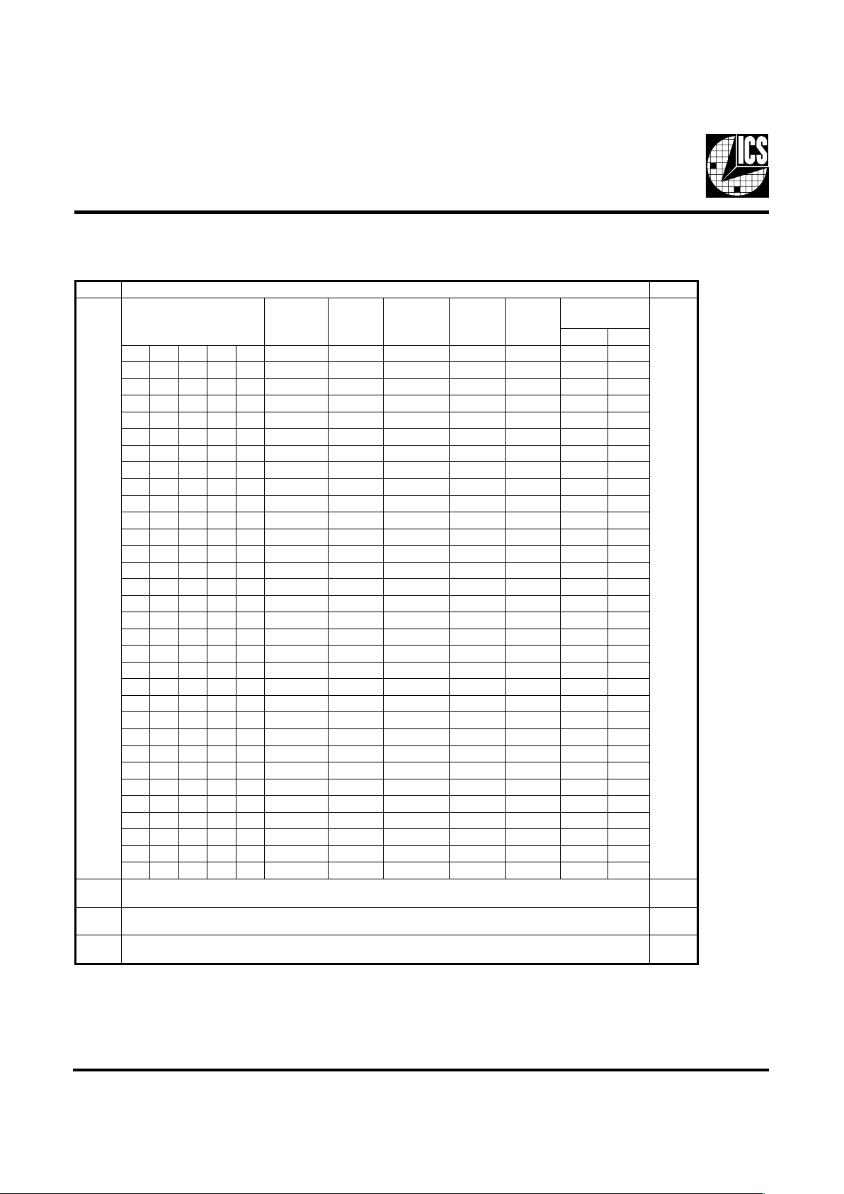
Byte4: Functionality and Frequency Select Register (default = 0)
Serial Configuration Command Bitmap
Note1: Default at power-up will be for latched logic inputs to define frequency, as displayed by Bit 3.
1) All entries selectable through I2C. Entries 1 -16 are also selectable through FS pins.
2) The IOAPIC Frequency change from IOAPIC=PCICLK/2 to IOAPIC=PCICLK is
controlled by IOAPC_Freq control in I2C Byte 3 Bit 1, default is IOAPIC=PCICLK/2.
3) Read back code of PWD shows revision ID.
I2C is a trademark of Philips Corporation
tiBnoitpircseDDWP
,2tiB
4:7tiB
)4:7,2(tiB
KLCUPC
)zHM(
/UPC
MARDS
MARDS
)zHM(
66V3
)zHM(
KLCICP
)zHM(
CIPAOI
)zHM(
00100
1etoN
2/ICP=ICP=
00000 3.3800.13.3884.5547.7278.3147.72
00001 00.42100.100.42176.2833.1476.0233.14
00010 00.55100.100.55133.30176.1538.5276.15
00011 69.34133.100.80100.2700.6300.8100.63
00100 00.0776.000.50100.0700.5305.7100.53
00101 00.21100.100.21176.4733.7376.8133.73
00110 00.05100.100.05100.00100.0500.5200.05
00111 00.04133.100.50100.0700.5305.7100.53
01000 33.8676.005.20133.8671.4380.7171.43
01001 00.70100.100.70133.1776.5338.7176.53
01010 00.83100.100.83100.2900.6400.3200.64
01011 33.73133.100.30176.8643.4371.7143.43
01100 08.6676.002.00108.6604.3307.6104.33
01101 03.00100.103.00108.6604.3307.6104.33
01110 06.33100.106.33170.9835.4472.2235.44
01111 06.33133.102.00108.6604.3307.6104.33
10000 00.54100.100.54176.6933.8471.4233.84
10001 00.04100.100.04133.3976.6433.3276.64
10010 00.63100.100.63176.0933.5476.2233.54
10011 00.03100.100.03176.6833.3476.1233.34
10100 00.92100.100.92100.6800.3405.1200.34
1010 1 00.72100.100.72176.4833.2471.1233.24
10110 00.12100.100.12176.0833.0471.0233.04
10111 00.91100.100.91133.9776.9338.9176.93
11000 00.71100.100.71100.8700.9305.9100.93
11001 00.41100.100.41100.6700.8300.9100.83
11010 00.01100.100.01133.3776.6333.8176.63
11011 00.50100.100.50100.0700.5305.7100.53
11100 33.5776.000.31133.5776.7338.8176.73
11101 33.35133.100.51176.6733.8371.9133.83
11110 36.05133.100.31133.5776.7338.8176.73
11111 36.64133.100.01133.3776.6333.8176.63
3tiB
stupnIdehctaL,tceleserawdrahybdetcelessiycneuqerF-0
4:7,2tiBybdetcelessiycneuqerF-1
0
1tiB
lamroN-0
daerpSretneC%52.0±delbanEmurtcepSdaerpS-1
1
0tiB
gninnuR-0
stuptuollaetatsirT-1
0
Page 5
5
ICS92 48-87
Preliminary Product Preview
Third party brands and names are the property of their respective owners.
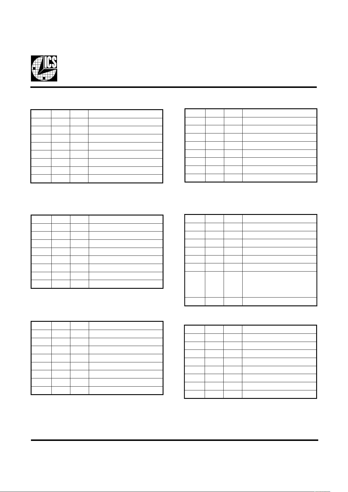
Byte 0: Control Register Active/Inactive Register
(1= enable, 0 = disable)
TIB#NIPDWPNOITPIRCSED
7tiB-0 devreseR
6tiB-0 devreseR
5tiB-0 devreseR
4tiB-0 devreseR
3tiB-0 devreseR
2tiB321 zHM84/42
1tiB22,121 zHM84
0tiB-0 devreseR
Notes:
1. Inactive means outputs are held LOW and are disabled
from switching.
2. Latched Frequency Selects (FS#) will be inverted logic
load of the input frequency select pin conditions.
3. SDRAM_F is free running and cannot be turned off by I
2
C
Byte 5: Peripheral , Active/Inactive Register
(1= enable, 0 = disable)
TIB#NIPDWPNOITPIRCSED
7tiB-0 devreseR
6tiB-0 devreseR
5tiB-0 devreseR
4tiB-0 devreseR
3tiB-0 devreseR
2tiB-0 devreseR
1tiB-0 devreseR
0tiB-0 devreseR
TIB#NIPDWPNOITPIRCSED
7tiB-0 )etoN(devreseR
6tiB-0 )etoN(devreseR
5tiB-0 )etoN(devreseR
4tiB-0 )etoN(devreseR
3tiB-0 )etoN(devreseR
2tiB-1 )etoN(devreseR
1tiB-1 )etoN(devreseR
0tiB-0 )etoN(devreseR
Byte 6: Peripheral , Active/Inactive Register
(1= enable, 0 = disable)
Note: Dont write into this register, writing into this
register can cause malfunction
Byte 2: PCI, Active/Inactive Register
(1= enable, 0 = disable)
TIB#NIPDWPNOITPIRCSED
7tiB911 7KLCICP
6tiB811 6KLCICP
5tiB711 5KLCICP
4tiB511 4KLCICP
3tiB411 3KLCICP
2tiB211 2KLCICP
1tiB111 1KLCICP
0tiB011 0KLCICP
Byte 3: Reserved , Active/Inactive Register
(1= enable, 0 = disable)
Byte 1: SDRAM, Active/Inactive Register
(1= enable, 0 = disable)
TIB#NIPDWPNOITPIRCSED
7tiB231 7MARDS
6tiB331 6MARDS
5tiB531 5MARDS
4tiB631 4MARDS
3tiB731 3MARDS
2tiB931 2MARDS
1tiB041 1MARDS
0tiB141 0MARDS
TIB#NIPDWPNOITPIRCSED
7tiB-0 devreseR
6tiB-X#2SF
5tiB-X#1SF
4tiB-X#0SF
3tiB-1 CIPAOI
2tiB-X #)#84_42LES(
1tiB-1
CIPAOI_QERF
2/KLCICP=CIPAOI>=1=
>=0=CIPAOI_QERF
KLCICP=CIPAOI
0tiB-X#3SF
Page 6
6
ICS9248-87
Preliminary Product Preview
Third party brands and names are the property of their respective owners.
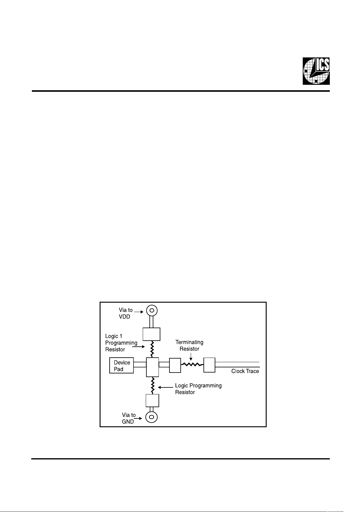
Shared Pin Operation Input/Output Pins
Fig. 1
The I/O pins designated by (input/output) on the ICS924887 serve as dual signal functions to the device. During initial
power-up, they act as input pins. The logic level (voltage)
that is present on these pins at this time is read and stored
into a 4-bit internal data latch. At the end of Power-On reset,
(see AC characteristics for timing values), the device changes
the mode of operations for these pins to an output function.
In this mode the pins produce the specified buffered clocks
to external loads.
To program (load) the internal configuration register for these
pins, a resistor is connected to either the VDD (logic 1)
power supply or the GND (logic 0) voltage potential. A 10
Kilohm(10K) resistor is used to provide both the solid CMOS
programming voltage needed during the power-up
programming period and to provide an insignificant load on
the output clock during the subsequent operating period.
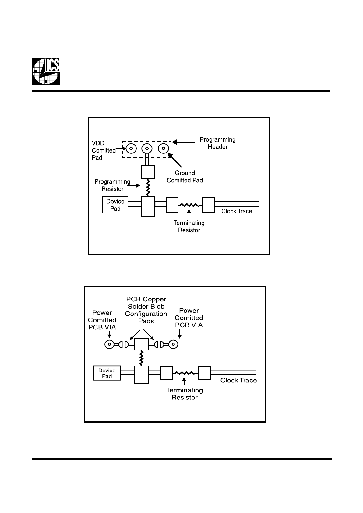
Figs. 1 and 2 show the recommended means of implementing
this function. In Fig. 1 either one of the resistors is loaded
onto the board (selective stuffing) to configure the devices
internal logic. Figs. 2a and b provide a single resistor loading
option where either solder spot tabs or a physical jumper
header may be used.
These figures illustrate the optimal PCB physical layout
options. These configuration resistors are of such a large
ohmic value that they do not effect the low impedance clock
signals. The layouts have been optimized to provide as little
impedance transition to the clock signal as possible, as it
passes through the programming resistor pad(s).
Page 7
7
ICS92 48-87
Preliminary Product Preview
Third party brands and names are the property of their respective owners.
Fig. 2a
Fig. 2b
Page 8
8
ICS9248-87
Preliminary Product Preview
Third party brands and names are the property of their respective owners.
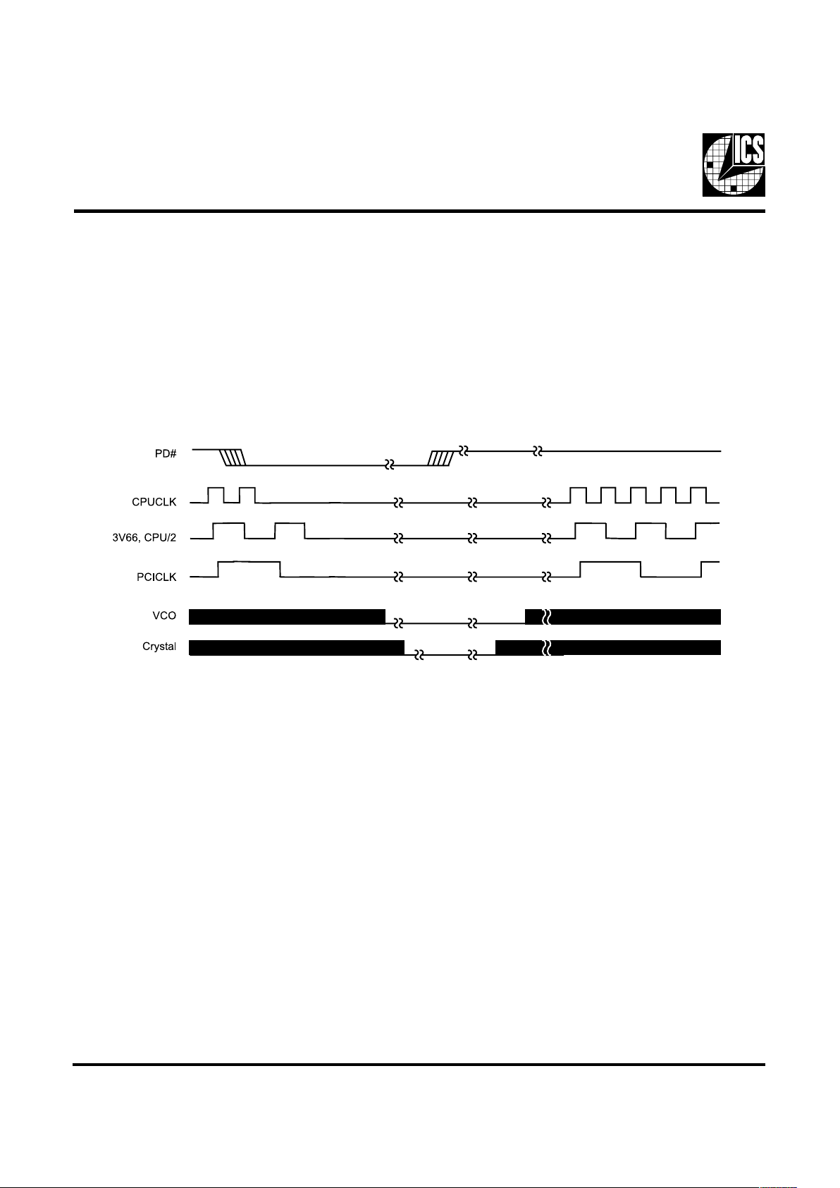
PD# Timing Diagram
The power down selection is used to put the part into a very low power state without turning off the power to the part. PD# is
an asynchronous active low input. This signal needs to be synchronized internal to the device prior to powering down the clock
synthesizer.
Internal clocks are not running after the device is put in power down. When PD# is active low all clocks need to be driven to a
low value and held prior to turning off the VCOs and crystal. The power up latency needs to be less than 3 mS. The power down
latency should be as short as possible but conforming to the sequence requirements shown below. PCI_STOP# and
CPU_STOP# are considered to be don't cares during the power down operations. The REF and 48MHz clocks are expected to
be stopped in the LOW state as soon as possible. Due to the state of the internal logic, stopping and holding the REF clock
outputs in the LOW state may require more than one clock cycle to complete.
Notes:
1. All timing is referenced to the Internal CPUCLK (defined as inside the ICS9248-87 device).
2. As shown, the outputs Stop Low on the next falling edge after PD# goes low.
3. PD# is an asynchronous input and metastable conditions may exist. This signal is synchronized inside this part.
4. The shaded sections on the VCO and the Crystal signals indicate an active clock.
5. Diagrams shown with respect to 133MHz. Similar operation when CPU is 100MHz.
Page 9
9
ICS92 48-87
Preliminary Product Preview
Third party brands and names are the property of their respective owners.
Absolute Maximum Ratings
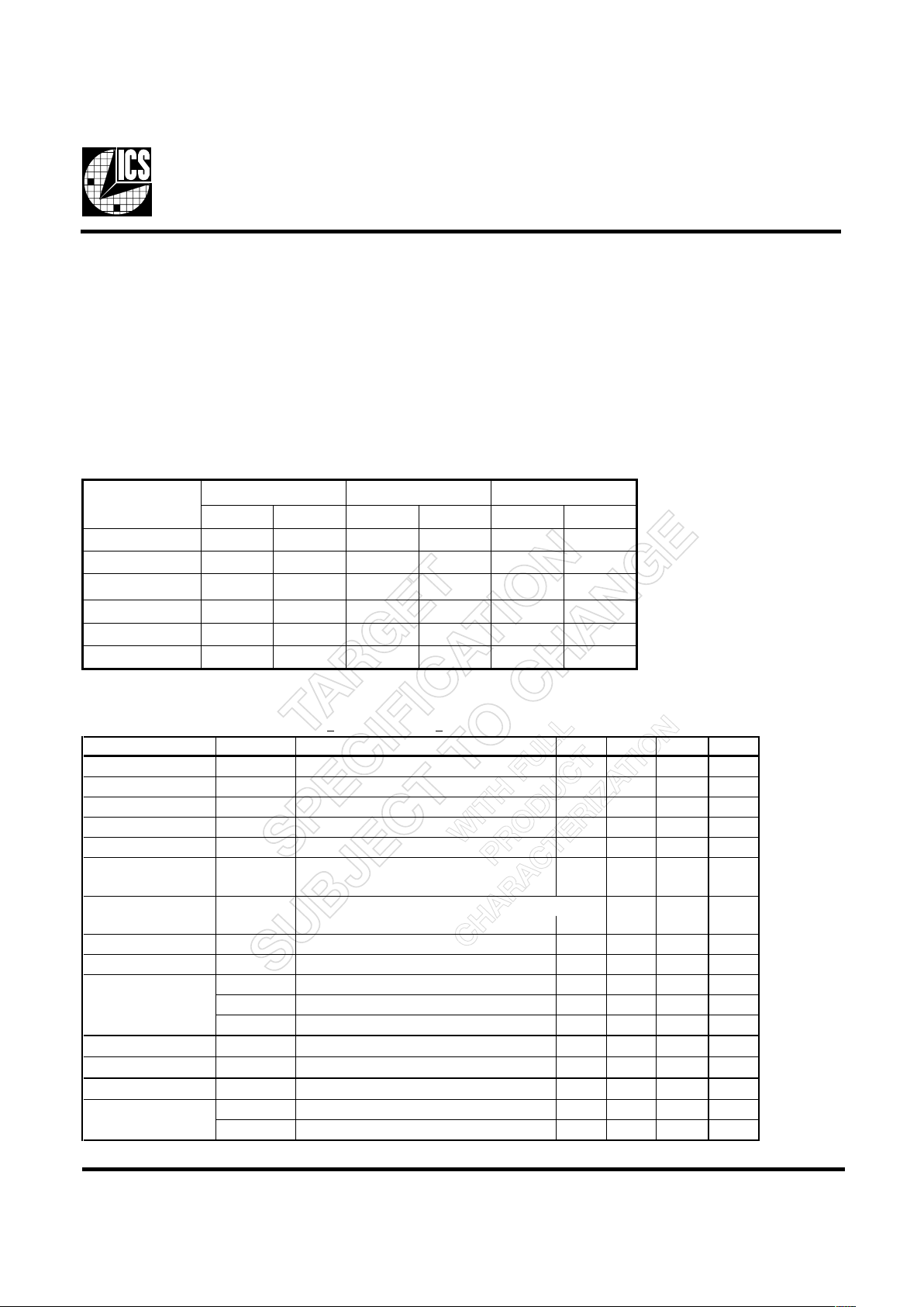
Core Supply Voltage . . . . . . . . . . . . . . . . . . . . . . . 4.6 V
I/O Supply Voltage . . . . . . . . . . . . . . . . . . . . . . . . . 3.6V
Logic Inputs . . . . . . . . . . . . . . . . . . . . . . . . . . . . . . GND 0.5 V to V
DD
+0.5 V
Ambient Operating Temperature . . . . . . . . . . . . . 0°C to +70°C
Storage Temperature . . . . . . . . . . . . . . . . . . . . . . . 65°C to +150°C
Stresses above those listed under Absolute Maximum Ratings may cause permanent damage to the device. These ratings are
stress specifications only and functional operation of the device at these or any other conditions above those listed in the
operational sections of the specifications is not implied. Exposure to absolute maximum rating conditions for extended periods
may affect product reliability.
Electrical Characteristics - Input/Supply/Common Output Parameters
TA = 0 - 70C ; S upply Voltage VDD = 3.3 V +5%, VDDL=2.5 V+ 5%( unless otherwise state d)
PARAMETER SYMBOL CONDITIONS MIN TYP MAX UNITS
Input High Volt age V
IH
2V
DD
+0.3 V
Input L ow V olt age V
IL
VSS-0.3 0.8 V
Input High Cur rent I
IH
VIN = V
DD
-5 5
µ
A
Input L ow Current I
IL1
VIN = 0 V; Inputs with no pull-up resistors -5 2.0
µ
A
Input L ow Current I
IL2
VIN = 0 V; Inputs with pull-up resistors -200 -100
µ
A
Operating I
DD3.3OP
CL = 0 pF; Select @ 66M 60 100 mA
Supply Current
Power Down I
DD3.3PD
CL = 0 pF; With input a ddress to Vdd or GND 400 600
µ
A
Supply Current
Input freque nc y F
i
VDD = 3. 3 V; 14.318 MHz
Pin Inductance L
pin
7nH
C
IN
Logic Inputs 5 pF
C
out
Out put pin ca pa cit anc e 6 pF
C
INX
X1 & X2 pins 27 45 pF
Transition Time
1
T
t
rans
To 1s t c ross ing of tar ge t Freq. 3 m S
Settling Time
1
T
s
From 1st c rossi ng to 1% t a rget Freq. 3 m S
Clk Sta biliz a tion
1
T
STAB
From VDD = 3.3 V to 1% t a rget Freq. 3 m S
Delay t
PZH,tPZH
output enable de l a y (all outputs ) 1 10 nS
t
PLZ,tPZH
output disable dela y (all outputs) 1 10 nS
1
Gua renteed by de sign, not 100% te sted in produc ti on.
Input C a pacitance
1
puorG
zHM66UPCzHM001UPCzHM331UPC
tesffOecnareloTtesffOecnareloTtesffOecnareloT
MARDSotUPCsn5.2sp005sn0.5sp005sn0.0sp005
66V3otUPCsn5.7sp005sn0.5sp005sn0.0sp005
66V3otMARDSsn0.0sp005sn0.0sp005sn0.0sp005
ICPot66V3sn5.3-5.1sp005sn5.3-5.1sp005sn5.3-5.1sp005
ICPotICPsn0.0sn0.1sn0.0sn0.1sn0.0sn0.1
TOD&BSUhcnysAA/NhcnysAA/NhcnysAA/N
Group Timing Relationship Table
Page 10
10
ICS9248-87
Preliminary Product Preview
Third party brands and names are the property of their respective owners.
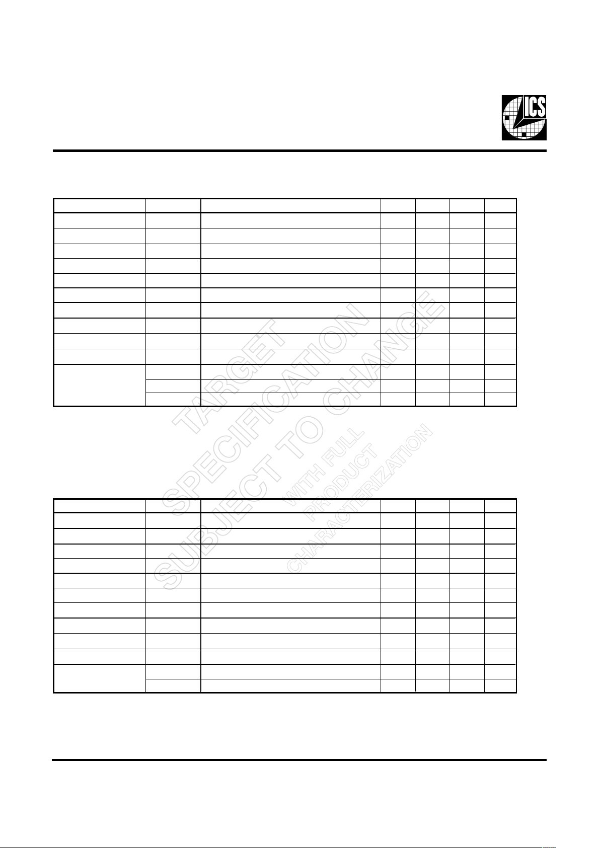
Electrical Characteristics - 3V66
TA = 0 - 70C; VDD = 3.3 V +/-5 % ; CL = 1 0-30 pF (unless oth erw is e s ta te d)
PARA METER SYMBOL CON D ITI O NS MIN TYP MAX UNI TS
O utput Impe da nc e R
DSP1
1
VO = VDD*(0.5) 12 55
Ω
O utput Impe da nc e R
DSN1
1
VO = VDD*(0.5) 12 55
Ω
Output High Voltage V
OH1
IOH = -1 mA 2.4 V
Output Low Voltage V
OL1
IOL = 1 mA 0.55 V
O utput High Cur r e nt I
OH1
VOH@ MIN = 1.0 V, VOH@ MAX = 3.135 V -33 -33 mA
O utput L o w Cur rent I
OL1
VOL@ MIN = 1.95 V, VOL@ MAX= 0.4 30 38 mA
Rise Time t
r1
1
VOL = 0. 4 V, VOH = 2.4 V 0.5 2 ns
F all T ime t
f1
1
VOH = 2.4 V, VOL = 0.4 V 0.5 2 ns
Duty Cycle d
t1
1
VT = 1.5 V 45 55 %
Skew t
sk1
1
VT = 1.5 V 175 ps
Jitter t
jcyc-cyc
VT = 1.5 V 500 ps
1
G ua renteed by de s ign, not 100% te s te d in production.
Electrical Characteristics - CPU
TA = 0 - 70C, V
DDL
= 2.5 V +/-5 % ; CL = 1 0 - 20 pF (unless othe rwis e stated)
PARA METER SYMBOL CON D ITI O NS MIN TYP MAX UNI TS
O utput Impe da nc e R
DSP2B
1
VO = VDD*(0.5) 13.5 45
Ω
O utput Impe da nc e R
DSN2B
1
VO = VDD*(0.5) 13.5 45
Ω
Output High Voltage V
OH2B
IOH = -1 mA 2 V
Output Low Voltage V
OL2B
IOL = 1 mA 0.4 V
O utput High Cur r e nt I
OH2B
V
OH @MIN
= 1.0V , V
OH@ MAX
= 2 . 375 V -27 -27 m A
O utput Low C urrent I
OL2B
V
OL @MIN
= 1. 2V , V
OL@ MAX
= 0. 3 V 27 30 mA
Rise Time t
r2B
1
VOL = 0. 4 V, VOH = 2 . 0 V 0.4 1.6 ns
F all T ime t
f2B
1
VOH = 0.4 V, VOL = 2 . 0 V 0.4 1.6 ns
Duty Cycle d
t2B
1
VT = 1.25 V 455055%
Skew t
s
k2B
1
VT = 1.25 V 175 ps
t
jcyc-cyc
1
VT = 1.25 V 250 ps
Jitter
1
G ua renteed by de s ign, not 100% te s te d in production.
Page 11
11
ICS92 48-87
Preliminary Product Preview
Third party brands and names are the property of their respective owners.
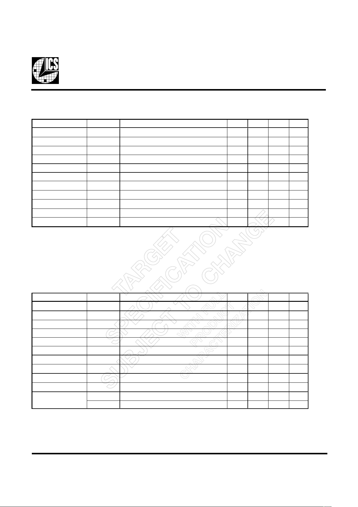
Electrical Characteristics - IOAPIC
TA = 0 - 70C;V
DDL
= 2. 5 V + /- 5% ; CL = 10 - 20 pF (unless otherwise state d)
PARA METER SYMBOL CONDITION S MIN TYP MAX UNITS
O utput Impe da nc e R
DSP4B
1
VO = VDD*(0.5) 9 30
Ω
O utput Impe da nc e R
DSN4B
1
VO = VDD*(0.5) 9 30
Ω
Output High Voltage V
OH4\ B
IOH = -5.5 mA 2 V
Output Low Voltage V
OL4B
IOL = 9.0 mA 0.4 V
O utput High Current I
OH4B
V
OH@ min
= 1.0 V, V
OH@ MAX
= 2 .375 V -27 -27 mA
O utput L o w Cur rent I
OL4B
V
OL@ MIN
= 1.2 V, V
OL@ MAX=
0.3V 27 30 mA
Rise Time t
r
4B
1
VOL = 0. 4 V, VOH = 2 .0 V 0.4 1.6 ns
Fa ll T ime t
f4B
1
VOH = 2.0 V, VOL = 0 .4 V 0.4 1.6 ns
Duty Cycle d
t4B
1
VT = 1.25 V 45 55 %
Jitter t
jcyc-cyc
VT = 1.25 V 500 ps
Skew
T
sk4
1
250 ps
1
G ua renteed by de s ign, not 100% te s te d in production.
Electrical Characteristics - SDRAM
TA = 0 - 70C; VDD = V
DDL
= 3.3 V +/-5%; CL = 20 - 30 pF (unless otherwise stated)
PARA METER SYMBOL CONDITION S MIN TYP MAX UNITS
O utput Impe da nc e R
DSP3
1
VO = VDD*(0.5) 10 24
Ω
O utput Impe da nc e R
DSN3
1
VO = VDD*(0.5) 10 24
Ω
Output High Voltage V
OH3
IOH = -1 mA 2.4 V
Output Low Voltage V
OL3
IOL = 1 mA 0.4 V
O utput High Cur r e nt I
OH3
V
OH @MIN
= 2.0 V, V
OH@ MAX
=3.135 V -54 -46 m A
Output Low Current I
OL3
V
OL@ MIN
= 1.0 V, V
OL@ MAX
=0.4 V 54 53 mA
Rise Time T
r
3
1
VOL = 0.4 V, VOH = 2.4 V 0.4 1.6 ns
Fa ll T ime T
f
3
1
VOH = 2.4 V, VOL = 0.4 V 0.4 1.6 ns
Duty Cycle D
t
3
1
VT = 1.5 V 45 55 %
Skew T
s
k3
1
VT = 1.5 V 250 ps
Jitter t
j
cyc-cyc VT = 1.5 V 250 ps
1
G ua renteed by de s ign, not 100% te s te d in production.
Page 12
12
ICS9248-87
Preliminary Product Preview
Third party brands and names are the property of their respective owners.
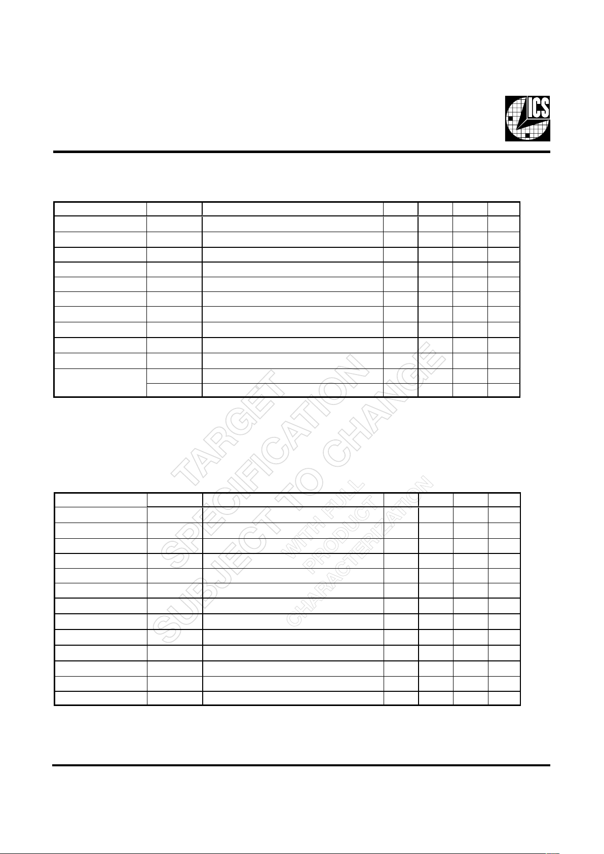
Electrical Characteristics - PCI
TA = 0 - 70C; VDD = 3.3 V +/-5 % ; CL = 1 0-30 pF (unless oth erw is e s ta te d)
PARA METER SYMBOL CON D ITI O NS MIN TYP MAX UNI TS
O utput Impe da nc e R
DSP1
1
VO = VDD*(0.5) 12 55
Ω
O utput Impe da nc e R
DSN1
1
VO = VDD*(0.5) 12 55
Ω
Output High Voltage V
OH1
IOH = -1 mA 2.4 V
Output Low Voltage V
OL1
IOL = 1 mA 0.55 V
O utput High Cur r e nt I
OH1
VOH@ MIN = 1.0 V, VOH@ MAX = 3.135 V -33 -33 mA
O utput L o w Cur rent I
OL1
VOL@ MIN = 1.95 V, VOL@ MAX= 0.4 30 38 mA
Rise Time t
r1
1
VOL = 0. 4 V, VOH = 2.4 V 0.5 2 ns
F all T ime t
f1
1
VOH = 2.4 V, VOL = 0.4 V 0.5 2 ns
Duty Cycle d
t1
1
VT = 1.5 V 45 55 %
Skew t
sk1
1
VT = 1.5 V 500 ps
Jitter t
jcyc-cyc
VT = 1.5 V 500 ps
1
G ua renteed by de s ign, not 100% te s te d in production.
Elect r ical Ch aract er ist ics - R EF, 48MHz_0 (Pi n 25)
TA = 0 - 70C; VDD = V
DDL
= 3.3 V +/-5%; CL = 10 -20 pF (unless otherwise state d)
PARA METER SYMBOL CON D ITIONS MIN TYP MAX UNITS
O utp ut I mpedanc e R
DSP5
1
VO = VDD*(0.5) 20 60
Ω
O utp ut I mpedanc e R
DSN5
1
VO = VDD*(0.5) 20 60
Ω
Output High Voltage V
OH5
IOH = 1 mA 2.4 V
Output Low Voltage V
OL5
IOL = -1 mA 0.4 V
O utput High Cur r e nt I
OH5
V
OH @MIN
=1 V, V
OH@MAX
= 3.135 V -29 -23 mA
O utput Low Cu r rent I
OL5
V
OL@MIN
=1.95 V, V
OL@MIN
=0.4 V 29 27 mA
Rise Time t
r5
1
VOL = 0. 4 V, VOH = 2.4 V 1.8 4 nS
F all Time t
f5
1
VOH = 2.4 V, VOL = 0.4 V 1.7 4 nS
Duty Cycle d
t5
1
VT = 1.5 V 45 55 %
Jitter t
jcyc-cyc
1
VT = 1.5 V; Fixed Cloc ks 500 pS
t
jcyc-cyc
1
VT = 1.5 V; R e f Clo cks 1000 pS
Skew T
sk
VT = 1.5 V 250 pS
1
G ua r e nte e d by de s ign, not 100% te s te d in production.
Page 13
13
ICS92 48-87
Preliminary Product Preview
Third party brands and names are the property of their respective owners.
Ordering Information
ICS9248yF-87
Pattern Number (2 or 3 digit number for parts with ROM code patterns)
Package Type
F=SSOP
Revision Designator (will not correlate with datasheet revision)
Device Type (consists of 3 or 4 digit numbers)
Prefix
ICS, AV = Standard Device
Example:
ICS XXXX y F - PPP
PRODUCT PREVIEW documents contain information on new
products in the sampling or preproduction phase of development.
Characteristic data and other specifications are subject to change
without notice.
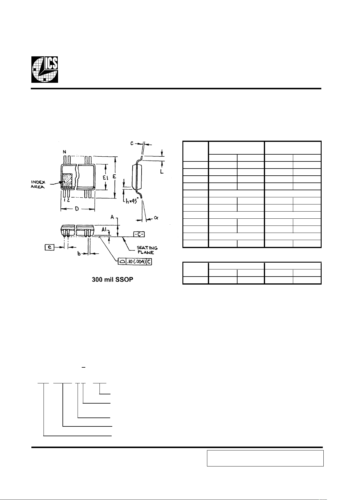
MIN MAX MIN MAX
A 2.413 2.794 .095 .110
A1 0.203 0.406 .008 .016
b 0.203 0.343 .008 .0135
c 0.127 0.254 .005 .010
D
E 10.033 10.668 .395 .420
E1 7.391 7.595 .291 .299
e 0.635 BASIC 0.025 BASIC
h 0.381 0.635 .015 .025
L 0.508 1.016 .020 .040
N
α
0° 8° 0° 8°
VARIATIONS
MIN MAX MIN MAX
48 15.748
16.002
.620 .630
JEDEC MO-118
DOC# 10-0034
6/1/00
REV B
N
D mm.
D (inch)
SEE VARIATIONS
SYMBOL
SEE VARIATIONS
SEE VARIATIONS
In Millimeters
COMMON DIMENSIONS
In Inches
COMMON DIMENSIONS
SEE VARIATIONS
 Loading...