

Page 1
Integrated
Circuit
Systems, Inc.
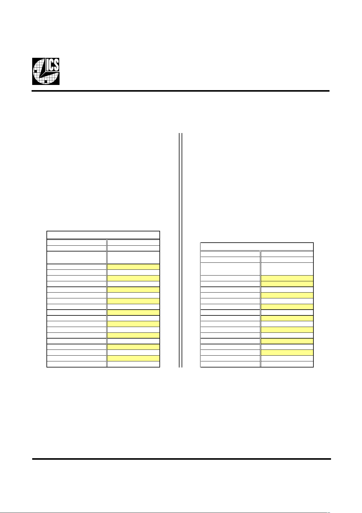
General Description Features
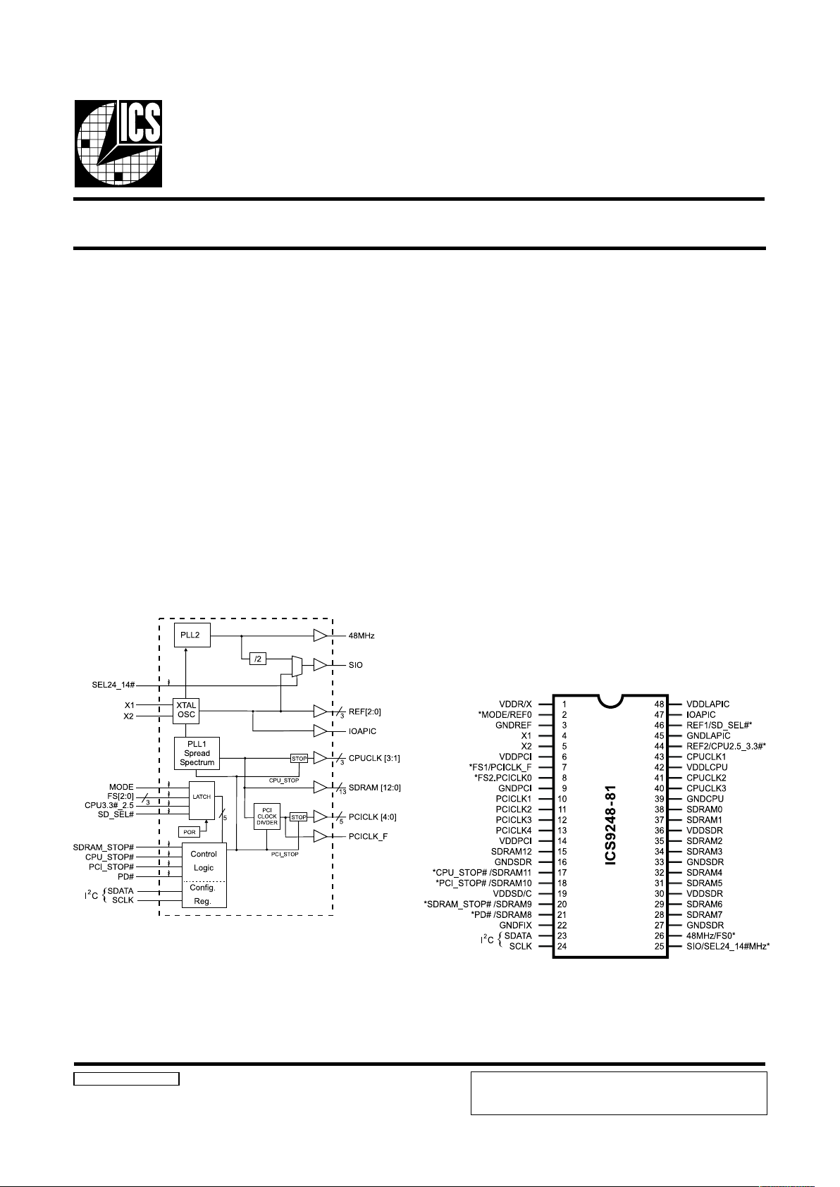
ICS9248 -81
Block Diagram
Pentium is a trademark of Intel Corporation
I2C is a trademark of Philips Corporation
Frequency Generator & Integrated Buffers
9248-81 Rev E 10/12/99
Pin Configuration
Generates the following system clocks:
- 3 CPU(2.5V/3.3V) up to 133.3MHz.
- 6 PCI(3.3V) (including 1 free-running)
- 13 SDRAMs(3.3V) up to 133.3MHz.
- 3 REF (3.3V) @ 14.318MHz
- 1 clock @ 24/14.3 MHz selectable output for SIO
- 1 Fixed clock at 48MHz (3.3V)
- 1 IOAPIC @ 2.5V / 3.3V
Skew characteristics:
- CPU CPU<175ps
- SDRAM SDRAM < 250ps
- CPUSDRAM < 500ps
- CPU(early) PCI : 1-4ns (typ. 3ns)
- PCI PCI <500ps
Supports Spread Spectrum modulation ±0.25 & ±0.5%
center spread
Serial I
2
C interface for Power Management, Frequency
Select, Spread Spectrum.
Efficient Power management scheme through PCI,
SDRAM, CPU STOP CLOCKS and PD#.
Uses external 14.318MHz crystal
48 pin 300mil SSOP.
48-Pin SSOP
Power Groups
VDDREF = REF [2:0], X1, X2
VDDPCI = PCICLK_F, PCICLK [4:0]
VDDSD/C = SDRAM [11:0], supply for PLL core, 24 MHz, 48MHz
VDD/CPU = CPUCLK [3:1]
VDDLAPIC = IOAPIC
GNDFIX = Ground for fixed clock PLL and output buffers
* Internal Pull-up Resistor of
120K to 3.3V on indicated inputs
The ICS9248-81 is the single chip clock solution for Desktop/
Notebook designs using the SIS style chipset. It provides all
necessary clock signals for such a system.
Spread spectrum may be enabled through I2C programming.
Spread spectrum typically reduces system EMI by 8dB to
10dB. This simplifies EMI qualification without resorting to
board design iterations or costly shielding. The ICS9248-81
employs a proprietary closed loop design, which tightly
controls the percentage of spreading over process and
temperature variations.
Serial programming I2C interface allows changing functions,
stop clock programming and frequency selection. The SD_SEL
latched input allows the SDRAM frequency to follow the
CPUCLK frequency(SD_SEL=1) or other clock frequencies
(SD_SEL=0)
ICS reserves the right to make changes in the device data identified in
this publication without further notice. ICS advises its customers to
obtain the latest version of all device data to verify that any
information being relied upon by the customer is current and accurate.
Page 2
2
ICS9248-81
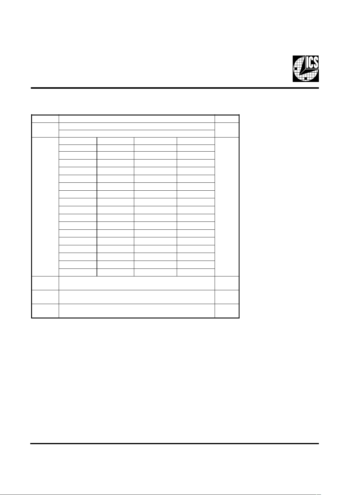
Pin Descriptions
Notes:
1: Internal Pull-up Resistor of 120K to 3.3V on indicated inputs
2: Bidirectional input/output pins, input logic levels are latched at internal power-on-reset. Use 10Kohm resistor
to program logic Hi to VDD or GND for logic low.
Pin number Pin name Type Description
1 VDDR /X Power Isolated 3. 3 V p ower f or c ryst al & referenc e
REF 0 Outp ut 3.3V , 14.318 MHz referenc e c loc k out put .
Mode Input Funct ion s ele c t pin, 1= des k t op m ode, 0= m obile m ode . Lat c hed input .
3,9,16, 22,
27,33, 39
GND Power 3.3 V Ground
4 X1 Input 14.318 M Hz c r
y
st al input
5 X2 Outp ut 14.318 M Hz c r
y
st al out put
6,14 VDDP C I Power 3 .3 V powe r for the P CI c loc k out puts
FS 1 Input Lo
g
ic input frequency select bit. Input lat c hed at power-on.
PCI CLK_F Outp ut 3.3 V free runnin
g
PCI c loc k outp ut, will not be s to pped by the PCI_STOP#
PCICLK 0 Output 3.3 V P CI c loc k outputs ,
g
enerating timing requirements for P entium I I
FS 2 Input Lo
g
ic input frequency select bit. Input lat c hed at power-on.
13, 12, 11, 10 PCI CLK [ 4:1] Outp ut 3.3 V P CI clo c k outpu ts , generati ng tim i ng requirem ents f or Pen tiu m II
15,28,29,31,32,
34,35,37,38
SDRA M 12,
SDRAM [7:0]
Outp ut SDRAM cl oc k outp uts . Frequency is s elec t ed by S D-Se l latc h ed input .
SDRA M 11 Output SD RA M c loc k out puts . Freque nc y is s elec t ed by S D-S el lat ch ed input .
CPU_ STO P# Input
As y nchronous act ive low input pin used to st op the CPUCLK in low state,
all other clock s will co ntinue to run. The CPUCLK will hav e a "Turnon" latenc y
of at leas t 3 CP U c loc k s .
SDRA M 10 Output SD RA M c loc k out put s . F re
q
uency is s ele ct ed by SD-SEL latched input.
PCI-STOP# Input
Sy nc h ronous ac tiv e l ow input us ed to st op t he P CI CLK in a low s t ate. I t will no t
effect PCICLK_F or an
y
other outputs.
19 V DDS D/ C Power 3.3 V pow er for SD RA M out puts and c o re
SDRA M 9 Out put S DRA M c loc k out put s . F re
q
uency is s ele ct ed by SD-Sel latc hed input.
SDRAM_STOP# Input
As y nchronous act ive low input used to s top the SDRA M in a low state.
It will not effect any other outputs.
SDRA M 8 Out put S DRA M c loc k out put s . F re
q
uency is s ele ct ed by SD-Sel latc hed input.
PD# Input
As y nchronous act ive low input pin used to power down the devic e into a low
power state. The internal cloc k s are disabled and the VCO and t he cry s tal are
stopped. The latenc
y
of the power down will not be greater than 3ms .
23 SDATA Input
Data input for I
2
C serial input .
24 SCLK Input
Clock input of I
2
C input
SE L24_14# Input
This input pin c ontrols the f requency of the S IO . I f logic 0 at power on
SIO=14.318 MHz . If lo
g
ic 1 at powe r-on S I O=24M Hz .
SIO Output Super I/O output. 24 or 14.318 MHz. S electable at power-up b
y
SE L24_14MHz
FS 0 I np ut Logic input f requency s elect bit . I nput lat ched at po wer-on.
48 MHz Output
3.3 V 48 M Hz c loc k out put , f ix ed f requenc y c loc k t ypi c ally us ed wit h
USB devic es
30,36 VDDS DR Power 3.3 V power for SDRAM out puts
40,41,43 CPUCLK [ 3:1] 0utput 2.5 V CPU and Hos t c loc k outputs
42 VDDLCPU Power 2.5 V power for CPU
REF 2 Outp ut 3.3V , 14.318 MHz referenc e c loc k out put .
CPU3 .3#_2.5 Inp ut
This pin s elect s t he operating voltage for the CPU. I f logic 0 at power on
CPU=3.3 V and i f logic 1 at powe r on CPU=2.5 V operat ing v olt age.
45 GNDL Power 2.5 V Ground for the IOAP IC or CPU
REF 1 Outp ut 3.3V , 14.318 MHz referenc e c loc k out put .
SD_SE L Input This input pin c ontrols the f re
q
uency of the SDRAM.
47 IOA P IC Output 2.5V fix ed 14.318 M Hz IOAPIC c loc k outputs
48 V DDLAPIC Power 2.5 V power for IOAPIC
2
1,2
8
1,2
26
1,2
7
1,2
46
1,2
44
1,2
17
1
20
1
18
1
21
1
25
1,2
Page 3
3
ICS9248-81
Power Management Functionality
Mode Pin - Power Management Input Control
CPU 3.3#_2.5V Buffer selector for CPUCLK drivers.
PD# CPU_STOP# PCI_STOP# SDRA M_STOP
PCICLK
(0:4)
SDRAM
(0:12)
PCICLK_F CPUCLK
Crystal
OSC
VCO
0X X X
Stopped
Low
Stopped
Low
Stopped
Low
Stopped
Low
Stopped
Low
Stopped
Low
1 1 1 1 Running Running Running Running Running Running
1 1 1 0 Running
Stopped
Low
Running Running Running Running
11 0 1
Stopped
Low
Running Running Running Running Running
11 0 0
Stopped
Low
Stopped
Low
Running Running Running Running
1 0 1 1 Running Running Running
Stopped
Low
Running Running
1 0 1 0 Running
Stopped
Low
Running
Stopped
Low
Running Running
10 0 1
Stopped
Low
Running Running
Stopped
Low
Running Running
10 0 0
Stopped
Low
Stopped
Low
Running
Stopped
Low
Running Running
2niP,EDOM
)tupnIdehctaL(
71niP81niP02niP12niP
0
#POTS_UPC
)TUPNI(
#POTS_ICP
)TUPNI(
#POTS_MARDS
)TUPNI(
#DP
)TUPNI(
1
11MARDS
)TUPTUO(
01MARDS
)TUPTUO(
9MARDS
)TUPTUO(
8MARDS
)TUPTUO(
5.2_#3.3UPC
leveltupnI
)ataDdehctaL(
detceleSreffuB
:tanoitareporof
1DDVV5.2
0DDVV3.3
Page 4
4
ICS9248-81
Functionality
VDD1, 2, 3, 4 = 3.3V±5%, V
DDL
= 2.5V ±5% or 3.3 ±5%, TA= 0 to 70°C
Crystal (X1, X2) = 14.31818MHz
SD_SEL FS2 FS1 FS0
CPU
MHZ
SDRAM
MHZ
PCI
MHZ
REF, IOAPIC
MHZ
0 0 0 0 90.00 90.00 30.00 14.318
0 0 0 1 66.70 100.05 33.35 14.318
0 0 1 0 95.00 63.33 31.66 14.318
0 0 1 1 100.00 66.66 33.33 14.318
0 1 0 0 100.00 75.00 30.00 14.318
0 1 0 1 112.00 74.66 37.33 14.318
0 1 1 0 124.00 82.66 31.00 14.318
0 1 1 1 133.30 88.86 33.32 14.318
1 0 0 0 66.70 66.70 33.35 14.318
1 0 0 1 75.00 75.00 30.00 14.318
1 0 1 0 83.30 83.30 33.32 14.318
1 0 1 1 95.00 95.00 31.66 14.318
1 1 0 0 100.00 100.00 33.33 14.318
1 1 0 1 112.00 112.00 37.33 14.318
1 1 1 0 124.00 124.00 31.00 14.318
1 1 1 1 133.30 133.30 33.33 14.318
Page 5
5
ICS9248-81
1. The ICS clock generator is a slave/receiver, I2C component. It can read back the data stored in the latches for verification.
Read-Back will support Intel PIIX4 "Block-Read" protocol.
2. The data transfer rate supported by this clock generator is 100K bits/sec or less (standard mode)
3. The input is operating at 3.3V logic levels.
4. The data byte format is 8 bit bytes.
5. To simplify the clock generator I2C interface, the protocol is set to use only "Block-Writes" from the controller. The
bytes must be accessed in sequential order from lowest to highest byte with the ability to stop after any complete byte
has been transferred. The Command code and Byte count shown above must be sent, but the data is ignored for those
two bytes. The data is loaded until a Stop sequence is issued.
6. At power-on, all registers are set to a default condition, as shown.
General I2C serial interface information
The information in this section assumes familiarity with I2C programming.
For more information, contact ICS for an I2C programming application note.
How to Write:
Controller (host) sends a start bit.
Controller (host) sends the write address D2
(H)
ICS clock will acknowledge
Controller (host) sends a dummy command code
ICS clock will acknowledge
Controller (host) sends a dummy byte count
ICS clock will acknowledge
Controller (host) starts sending first byte (Byte 0)
through byte 5
ICS clock will acknowledge each byte one at a time.
Controller (host) sends a Stop bit
How to Read:
Controller (host) will send start bit.
Controller (host) sends the read address D3
(H)
ICS clock will acknowledge
ICS clock will send the byte count
Controller (host) acknowledges
ICS clock sends first byte (Byte 0) through byte 5
Controller (host) will need to acknowledge each byte
Controller (host) will send a stop bit
Notes:
Controller (Host) ICS (Slave/Receiver)
Start Bit
Address
D3
(H)
AC
K
Byte Count
ACK
Byte
0
ACK
Byte 1
ACK
Byte
2
ACK
Byte
3
ACK
Byte 4
ACK
Byte
5
ACK
Stop Bit
How to Read:
Controller (Host) ICS (Slave/Receiver)
Start Bit
Address
D2
(H)
AC
K
Dummy Command Code
AC
K
Dummy Byte Count
AC
K
Byte 0
AC
K
Byte 1
ACK
Byte 2
AC
K
Byte 3
AC
K
Byte 4
AC
K
Byte 5
AC
K
Stop Bit
How to Write:
Page 6
6
ICS9248-81
Byte 0: Functionality and frequency select register (Default = 0)
Serial Configuration Command Bitmap
Note 1: Default at power-up will be for latched logic inputs to define frequency.
Note 2: PWD = Power-Up Default
tiB
noitpircseD
DWP
7tiB
murtcepSdaerpSretneC%52.0±-0
1
murtcepSdaerpSretneC%5.0±-1
tiB
)4:6,2(
)4:6,2(tiBKLCUPCMARDSKLCICP
XXXX
1etoN
000000.09
00.09
00.03
100007.66
50.001
53.33
010000.59
33.36
66.13
110000.001
66.66
33.33
001000.001
00.57
00.03
101000.211
66.47
33.73
011000.421
66.28
00.13
111003.331
68.88
23.33
000107.66
07.66
53.33
100100.57
00.57
00.03
010103.38
03.38
23.33
110100.59
00.59
66.13
001100.001
00.001
33.33
101100.211
00.211
33.73
011100.421
00.421
00.13
111103.331
03.331
33.33
3tiB
stupnidehctal,tceleserawdrahybdetcelessiycneuqerF-0
4:6,2tiBybdetcelessiycneuqerF-1
0
1tiB
lamroN-0
delbanemurtcepsdaerpS-1
1
0tiB
gninnuR-0
stuptuollaetatsirT-1
0
Page 7

7
ICS9248-81
Byte 1: CPU, Active/Inactive Register
(1 = enable, 0 = disable)
Byte 2: PCI Active/Inactive Register
(1 = enable, 0 = disable)
Byte 3: SDRAM Active/Inactive Register
(1 = enable, 0 = disable)
Notes:
1. Inactive means outputs are held LOW and are disabled
from switching.
Notes:
1. Inactive means outputs are held LOW and are disabled
from switching.
Notes:
1. Inactive means outputs are held LOW and are disabled
from switching.
Byte 4: SDRAM Active/Inactive Register
(1 = enable, 0 = disable)
Byte 5: Peripheral Active/Inactive
Register (1 = enable, 0 = disable)
Notes:
1. Inactive means outputs are held LOW and are disabled
from switching.
Notes:
1. Inactive means outputs are held LOW and are disabled
from switching.
tiB#niPDWPnoitpircseD
7tiB-1 )devreseR(
6tiB-1 )devreseR(
5tiB-1 )devreseR(
4tiB-1 )devreseR(
3tiB041 3KLCUPC
2tiB141 2KLCUPC
1tiB341 1KLCUPC
0tiB-X#0SF
tiB#niPDWPnoitpircseD
7tiB-X#1SF
6tiB71 F_KLCICP
5tiB-1 )devreseR(
4tiB311 4KLCICP
3tiB211 3KLCICP
2tiB111 2KLCICP
1tiB011 1KLCICP
0tiB81 0KLCICP
tiB#niPDWPnoitpircseD
7tiB821 7MARDS
6tiB921 6MARDS
5tiB131 5MARDS
4tiB231 4MARDS
3tiB431 3MARDS
2tiB531 2MARDS
1tiB731 1MARDS
0tiB831 0MARDS
tiB#niPDWPnoitpircseD
7tiB-1 )devreseR(
6tiB-X#2SF
5tiB-1 )devreseR(
4tiB741 CIPAOI
3tiB-X #LES_DS
2tiB4412FER
1tiB6411FER
0tiB210FER
tiB#niPDWPnoitpircseD
7tiB-1 )devreseR(
6tiB521 zHM41/42
5tiB621 zHM84
4tiB511 21MARDS
3tiB711 11MARDS
2tiB811 01MARDS
1tiB021 9MARDS
0tiB121 8MARDS
Page 8

8
ICS9248-81
CPU_STOP# Timing Diagram
CPU_STOP# is an asychronous input to the clock synthesizer. It is used to turn off the CPU clocks for low power operation.
CPU_STOP# is synchronized by the ICS9248-81. The minimum that the CPU clock is enabled (CPU_STOP# high pulse) is
100 CPU clocks. All other clocks will continue to run while the CPU clocks are disabled. The CPU clocks will always be
stopped in a low state and start in such a manner that guarantees the high pulse width is a full pulse. CPU clock on latency is
less than 4 CPU clocks and CPU clock off latency is less than 4 CPU clocks.
Notes:
1. All timing is referenced to the internal CPU clock.
2. CPU_STOP# is an asynchronous input and metastable conditions may exist. This signal is synchronized
to the CPU clocks inside the ICS9248-81.
3. All other clocks continue to run undisturbed. (including SDRAM outputs).
Page 9

9
ICS9248-81
SDRAM_STOP# Timing Diagram
SDRAM_STOP# is an sychronous input to the clock synthesizer. It is used to turn off the CPU clocks for low power operation.
SDRAM_STOP# is synchronized by the ICS9248-81. All other clocks will continue to run while the SDRAM clocks are
disabled. The SDRAM clocks will always be stopped in a low state and start in such a manner that guarantees the high pulse
width is a full pulse.
Notes:
1. All timing is referenced to the internal CPU clock.
2. SDRAM is an asynchronous input and metastable conditions may exist. This signal is synchronized to
the SDRAM clocks inside the ICS9248-81.
3. All other clocks continue to run undisturbed.
Page 10

10
ICS9248-81
PCI_STOP# Timing Diagram
PCI_STOP# is an synchronous input to the ICS9248-81. It is used to turn off the PCICLK (0:4) clocks for low power operation.
PCI_STOP# is synchronized by the ICS9248-81 internally. The minimum that the PCICLK (0:4) clocks are enabled
(PCI_STOP# high pulse) is at least 10 PCICLK (0:4) clocks. PCICLK (0:4) clocks are stopped in a low state and started with
a full high pulse width guaranteed. PCICLK (0:4) clock on latency cycles are only one rising PCICLK clock off latency is one
PCICLK clock.
Notes:
1. All timing is referenced to the Internal CPUCLK (defined as inside the ICS9248 device.)
2. PCI_STOP# is an asynchronous input, and metastable conditions may exist. This signal is required to be synchronized
inside the ICS9248.
3. All other clocks continue to run undisturbed.
4. CPU_STOP# is shown in a high (true) state.
Page 11

11
ICS9248-81
The I/O pins designated by (input/output) on the ICS924881 serve as dual signal functions to the device. During initial
power-up, they act as input pins. The logic level (voltage)
that is present on these pins at this time is read and stored
into a 4-bit internal data latch. At the end of Power-On reset,
(see AC characteristics for timing values), the device changes
the mode of operations for these pins to an output function.
In this mode the pins produce the specified buffered clocks
to external loads.
To program (load) the internal configuration register for
these pins, a resistor is connected to either the VDD (logic 1)
power supply or the GND (logic 0) voltage potential. A 10
Kilohm(10K) resistor is used to provide both the solid CMOS
programming voltage needed during the power-up
programming period and to provide an insignificant load on
the output clock during the subsequent operating period.
Figs. 1 and 2 show the recommended means of implementing
this function. In Fig. 1 either one of the resistors is loaded
onto the board (selective stuffing) to configure the devices
internal logic. Figs. 2a and b provide a single resistor loading
option where either solder spot tabs or a physical jumper
Shared Pin Operation Input/Output Pins
Fig. 1
header may be used.
These figures illustrate the optimal PCB physical layout
options. These configuration resistors are of such a large
ohmic value that they do not effect the low impedance clock
signals. The layouts have been optimized to provide as little
impedance transition to the clock signal as possible, as it
passes through the programming resistor pad(s).
Page 12

12
ICS9248-81
Fig. 2a
Fig. 2b
Page 13

13
ICS9248-81
Absolute Maximum Ratings
Supply Voltage . . . . . . . . . . . . . . . . . . . . . . . . . . . 5.5 V
Logic Inputs . . . . . . . . . . . . . . . . . . . . . . . . . . . . GND 0.5 V to V
DD
+0.5 V
Ambient Operating Temperature . . . . . . . . . . . . 0°C to +70°C
Storage Temperature . . . . . . . . . . . . . . . . . . . . . . 65°C to +150°C
Case Temperature . . . . . . . . . . . . . . . . . . . . . . . . 115°C
Stresses above those listed under Absolute Maximum Ratings may cause permanent damage to the device. These ratings are
stress specifications only and functional operation of the device at these or any other conditions above those listed in the
operational sections of the specifications is not implied. Exposure to absolute maximum rating conditions for extended periods
may affect product reliability.
Elect rical Charact eristics - I nput /Suppl y/ Com m o n Ou tput Param et ers
TA = 0 - 70C; Supply V oltage VDD = 3.3 V +/-5%, V
DDL
= 2 . 5 V +/-5% (unless otherw i se stated)
PARAMETER SY MBOL CONDITIONS MIN TY P MAX UNITS
Operating I
DD2.5OP66
CL = 0 pF; Select @ 66.8 MHz 16 72 mA
Suppl y Cur r ent I
DD2.5OP100
CL = 0 pF; Select @ 100 MHz 23 100 m A
t
CPU-SDRAM2
VT = 1.5 V; VTL = 1.25 V 200 500 ps
t
CPU-PCI2
VT = 1.5 V; VTL = 1.25 V
134ns
1
G uaranteed by design, not 100% tested in production.
Skew
1
Electrical Characteristics - I nput/Supply/Common Output Parameters
TA = 0 - 70C; Supply Voltage VDD = V
DDL
= 3.3 V +/-5% (unless othe rwise stated)
PARAMETER SYMBOL CONDITIONS MIN TYP MAX UNITS
Input High Voltage V
IH
2V
DD
+0.3 V
Input Low Voltage V
IL
VSS-0.3 0.8 V
Input High Current I
IH
VIN = V
DD
0.1 5
µ
A
Input Low Current I
IL1
VIN = 0 V; Inputs with no pull-up resistors -5 2.0
µ
A
Input Low Current I
IL2
VIN = 0 V; Inputs with pull-up resistors -200 -100
µ
A
Operating I
DD3.3OP66CL
= 0 pF; Select @ 66MHz 60 180 mA
Supply Current I
DD3.3OP100CL
= 0 pF; Select @ 100MHz 66 180 mA
Power Down I
DD3.3PD
CL = 0 pF; With input address to Vdd or GND 70 600
µ
A
Supply Current
Input frequency F
i
VDD = 3.3 V; 11 14.318 16 M Hz
Input Capacitance
1
C
IN
Logic Inputs 5 pF
C
INX
X1 & X2 pins 27 36 45 pF
Transition Time
1
T
trans
To 1st crossing of target Freq. 3 ms
Clk Stabilization
1
T
STAB
From VDD = 3.3 V to 1% target Freq. 3 ms
t
CPU-SDRAM1VT
= 1.5 V 200 500 ps
t
CPU-PCI1
VT = 1.5 V
134ns
1
Guaranteed by design, not 100% tested in production.
Skew
1
Page 14

14
ICS9248-81
Electrical Characteristics - CPUCLK
TA = 0 - 70C; VDD = VDDL = 3.3 V +/-5%; CL = 10 - 20 pF (unless otherwise stated)
PARAMETER SYMBOL CONDITIONS MIN TYP MAX UNITS
Output High Voltage V
OH1a
IOH = -12.0 mA 2.4 2.6 V
Output Low Voltage V
OL1
a
IOL = 12 mA 0.2 0.4 V
Output High Current I
OH1a
VOH = 2 V -41 -19 mA
Output Low Current I
OL1
a
VOL = 0.8 V 19 37 mA
Rise Time t
r1
a
1
VOL = 0.4 V, VOH = 2.4 V 1.5 2 ns
Fall Time t
f1
a
1
VOH = 2.4 V, VOL = 0.4 V 1.5 2 ns
Duty Cycle d
t1
a
1
VT = 1.5 V 45 48 55 %
Skew t
sk1
a
1
VT = 1.5 V 30 175 ps
Jitter, Cycle-to-cycle t
jcy
c-cyc1a
1
VT = 1.5 V 150 250 ps
Jitter, One Sigma t
j
1s1
a
1
VT = 1.5 V 40 150 ps
Jitter, Absolute
t
jabs1a
1
VT = 1.5 V
-250 140 +250 ps
1
Guaranteed by design, not 100% tested in production.
Electrical Characteristics - CPUCLK
TA = 0 - 70C; VDD = 3.3 V +/-5%, V
DDL
= 2.5 V +/-5%; CL = 10 - 20 pF (unless otherwi se stated)
PARAMETER SYMBOL CONDITIONS MIN TYP MAX UNITS
Output High Voltage V
OH1B
IOH = -12.0 mA 2 2.3 V
Output Low Voltage V
OL1B
IOL = 12 mA 0.2 0.4 V
Output High Current I
OH1B
VOH = 1.7 V -41 -19 mA
Output Low Current I
OL1B
VOL = 0.7 V 19 37 mA
Rise Time t
r1B
1
VOL = 0.4 V, VOH = 2.0 V 1.25 1.6 ns
Fall Time t
f1B
1
VOH = 2.0 V, VOL = 0.4 V 1 1.6 ns
Duty Cycle d
t1B
1
VT = 1.25 V 45 48 55 %
Skew t
sk1B
1
VT = 1.25 V 30 175 ps
Jitter, Cycle-to-cycle t
jcy
c-cyc1B
1
VT = 1.25 V 150 250 ps
Jitter, One Sigma t
j
1s1B
1
VT = 1.25 V 40 150 ps
Jitter, Absolute
t
jabs1B
1
VT = 1.25 V
-250 140 +250 ps
1
Guaranteed by design, not 100% tested in production.
Page 15

15
ICS9248-81
Electrical Characteristics - PCICLK
TA = 0 - 70C; VDD = 3.3 V +/-5%; V
DDL
= 2.5 V +/-5%; CL = 30 pF
PARAMETER SYMBOL CONDITIONS MIN T YP MAX UNITS
Output High Voltage V
OH2
IOH = -11 mA 2.4 3.1 V
Output Low Voltage V
OL2
IOL = 9.4 mA 0.1 0.4 V
Output High Current I
OH2
VOH = 2.0 V -62 -22 mA
Output Low Current I
OL2
VOL = 0.8 V 16 57 mA
Rise Time
1
t
r2
VOL = 0.4 V, VOH = 2.4 V 1.5 2.6 ns
Fall Time
1
t
f2
VOH = 2.4 V, VOL = 0.4 V 1.1 2 ns
Duty Cycle
1
d
t2
VT = 1.5 V 45 50 55 %
Skew
1
t
sk2
VT = 1.5 V 140 500 ps
Jitter, Cycle-to-cycle t
jcy
c-cyc2
VT = 1.25 V 250 500 ps
Jitter, One Sigma
1
t
j
1s2
VT = 1.5 V 17 150 ps
Jitter, Absolute
1
t
jabs2
VT = 1.5 V
-350 70 350 ps
1
Guaranteed by design, not 100% tested in production.
Electrical Characteristics -SDRAM
TA = 0 - 70C; VDD = 3.3 V +/-5%; V
DDL
= 2.5 V +/-5%; CL = 30 pF
PARAMETER SYMBOL CONDITIONS MIN TYP MAX UNITS
Output High Volt age V
OH3
IOH = -11 mA 2.4 3.1 V
Output Low Voltage V
OL3
IOL = 9.4 mA 0.1 0.4 V
Output High Current I
OH3
VOH = 2.0 V -62 -22 mA
Output Low Current I
OL3
VOL = 0.8 V 16 57 mA
Rise Time
1
t
r3
VOL = 0.4 V, VOH = 2.4 V 1.5 2.6 ns
Fall Time
1
t
f3
VOH = 2.4 V, VOL = 0.4 V 1.1 2.2 ns
d
t3a
VT = 1.5 V; Divide by 2 seclects<124MHz 47% 57%
d
t3b
VT = 1.5 V; Divide by 3 seclects 45 55
d
t3c
VT = 1.5 V; Selects >= 124MHz 43 50 53 %
t
sk3a
VT = 1.5 V; SDRAM0,8,9
t
sk3b
VT = 1.5 V; All except SDRAM8 and 9
t
sk3c
VT = 1.5 V; All SDRAMs
200 400
Jitter, Cycle-to-cycle t
jcy
c-cyc3
VT = 1.25 V 250 500 ps
Jitter, One Sigma
1
t
j
1s3
VT = 1.5 V 17 150 ps
Jitter, Absolute
1
t
jabs3
VT = 1.5 V
-250 70 250 ps
1
Guaranteed by design, not 100% tested in production.
Duty Cycle
1
ps
Skew
1
(Window)
250140
Page 16

16
ICS9248-81
Ele ctrical Charact eristics - REF/48MH z/SI O
TA = 0 - 70C; VDD = 3.3 V +/-5%; V
DDL
= 2.5 V +/-5%; CL = 20 pF
PARAMETER SYMBOL CONDITIONS MIN TY P MAX UNITS
O utput High Voltage V
OH4
IOH = -12 mA 2.4 2.6 V
Output Low Voltage V
OL4
IOL = 10 mA 0.3 0.4 V
Ou tput High Current I
OH4
VOH = 2.0 V -32 -22 mA
Output L ow Current I
OL4
VOL = 0.8 V 16 25 m A
Rise Time
1
t
r4
VOL = 0.4 V, VOH = 2.4 V 2 4 ns
Fall Time
1
t
f4
VOH = 2.4 V , VOL = 0.4 V 1.9 4 ns
Duty Cycle
1
d
t4
VT = 1.5 V 45 53 55 %
Jitter, O ne Si gma
1
t
j1s4
VT = 1.5 V 500 650 ps
Jitter, Absolute
1
t
jabs4
VT = 1.5 V
-1 1 ns
1
Guara nt eed by design, no t 100% tested in production.
Page 17

17
ICS9248-81
General Layout Precautions:
1) Use a ground plane on the top layer
of the PCB in all areas not used by
traces.
2) Make all power traces and ground
traces as wide as the via pad for lower
inductance.
Notes:
1) All clock outputs should have a
series terminating resistor, and a 20pF
capacitor to ground between the
resistor and clock pin. Not shown in
all places to improve readibility of
diagram.
2) Optional crystal load capacitors are
recommended. They should be
included in the layout but not inserted
unless needed.
Connections to VDD:
C1
C1
C4
1
Clock Load
C3
C3
48
47
46
45
44
43
42
41
40
39
38
37
36
35
34
33
32
31
30
29
28
27
26
25
1
2
3
4
5
6
7
8
Ferrite
Bead
VDD
C2
22µF/20V
Tantalum
Ferrite
Bead
VDD
C2
22µF/20V
Tantalum
1
2
3
4
5
6
7
8
9
10
11
12
13
14
15
16
17
18
19
20
21
22
23
24
= Routed Power
= Ground Connection Key (component side copper)
= Ground Plane Connection
= Power Route Connection
= Solder Pads
= Clock Load
Ground
2.5V Power Route
3.3V Power Route
3.3V Power Route
Page 18

18
ICS9248-81
SSOP Package
LOBMYS SNOISNEMIDNOMMOC SNOITAIRAV D N
.NIM.MON.XAM.NIM.MON.XAM
A590.101.011.CA026.526.036.84
1A800.210.610.
2A880.090.290.
B800.010.5310.
C500.- 010.
DsnoitairaVeeS
E292.692.992.
eCSB520.0
H004.604.014.
h010.310.610.
L420.230.040.
NsnoitairaVeeS
µ
°0°5 °8
X580.390.001.
Ordering Information
ICS9248yF-81
Pattern Number (2 or 3 digit number for parts with ROM code patterns)
Package Type
F=SSOP
Revision Designator
Device Type (consists of 3 or 4 digit numbers)
Prefix
ICS, AV = Standard Device
Example:
ICS XXXX y F - PPP
ICS reserves the right to make changes in the device data identified in
this publication without further notice. ICS advises its customers to
obtain the latest version of all device data to verify that any
information being relied upon by the customer is current and accurate.
 Loading...