

Page 1
Integrated
Circuit
Systems, Inc.
General Description
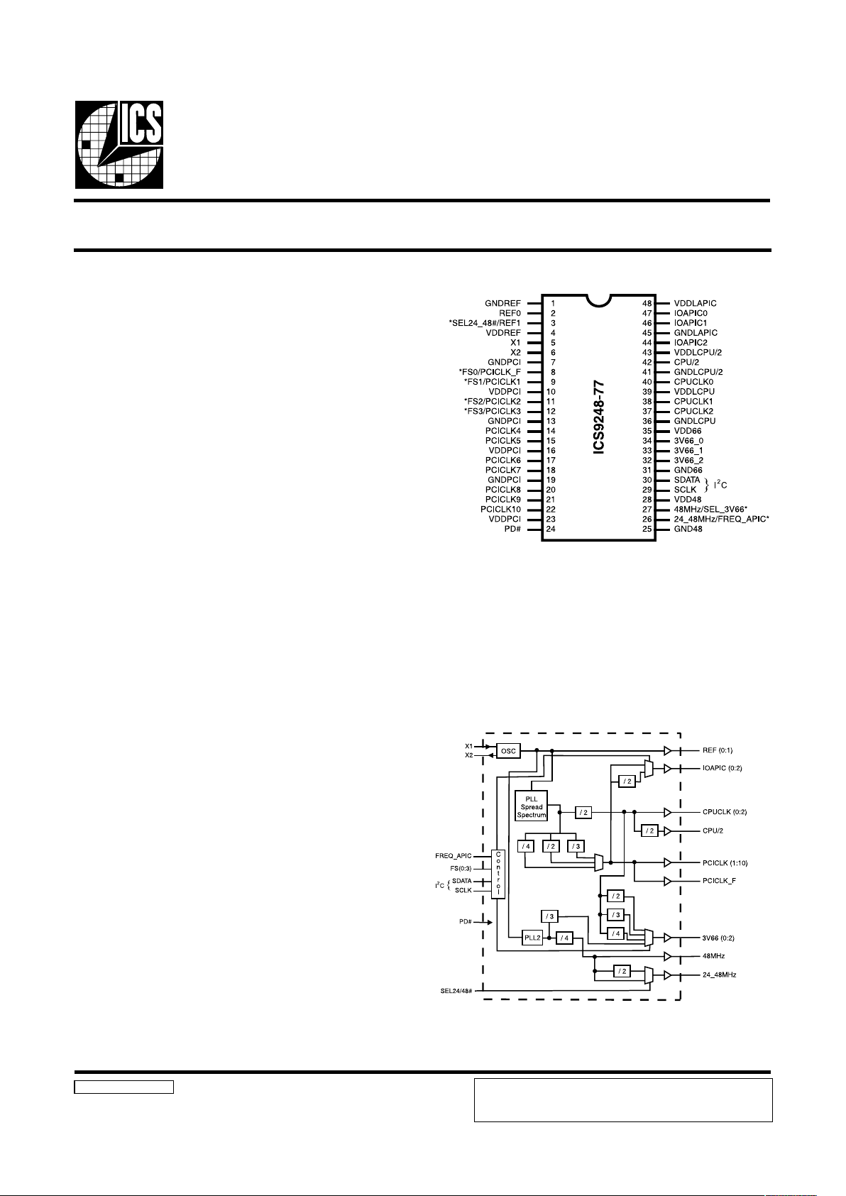
ICS9248-77
Block Diagram
Frequency Timing Generator for PENTIUM II Systems
9248-77 Rev C 10/20/99
Pin Configuration
48-pin SSOP
*120K ohm pull-up to VDD on indicated inputs.
Generates the following system clocks:
- 3 - CPUs @ 2.5V, up to 150MHz.
- 3 - IOAPIC @ 2.5V, PCI or PCI/2
- 3 - 3V66MHz @ 3.3V.
- 11 - PCIs @ 3.3V.
- 1 - 48MHz, @ 3.3V fixed.
- 1 - 24MHz, @ 3.3V fixed.
- 1 - CPU/2, @ 2.5V.
± .25% center spread, or 0 to -.5% down spread.
Uses external 14.318MHz crystal.
The ICS9248-77 is a main clock synthesizer chip for Pentium
II based systems using Rambus Interface DRAMs. This chip
provides all the clocks required for such a system when used
with a Direct Rambus Clock Generator(DRCG) chip such as
the ICS9212-01.
Spread Spectrum may be enabled by driving the SPREAD#
pin active. Spread spectrum typically reduces system EMI by
8dB to 10dB. This simplifies EMI qualification without resorting
to board design iterations or costly shielding. The ICS9248-
77 employs a proprietary closed loop design, which tightly
controls the percentage of spreading over process and
temperature variations.
The CPU/2 clocks are inputs to the DRCG.
ICS reserves the right to make changes in the device data identified in
this publication without further notice. ICS advises its customers to
obtain the latest version of all device data to verify that any
information being relied upon by the customer is current and accurate.
Features
Key Specification
CPU Output Jitter: <250ps
CPU/2 Output Jitter. <250ps
IOAPIC Output Jitter: <500ps
48MHz, 3V66, PCI Output Jitter: <500ps
Ref Output Jitter. <1000ps
CPU Output Skew: <175ps
IOAPIC Output Skew <250ps
PCI Output Skew: <500ps
3V66 Output Skew <250ps
CPU to 3V66 Output Offset: 0.0 - 1.5ns (CPU leads)
3V66 to PCI Output Offset: 1.5 - 4.0ns (3V66 leads)
CPU to IOAPIC Output Offset 1.5 - 4.0ns (CPU leads)
Page 2
2
ICS9248-77
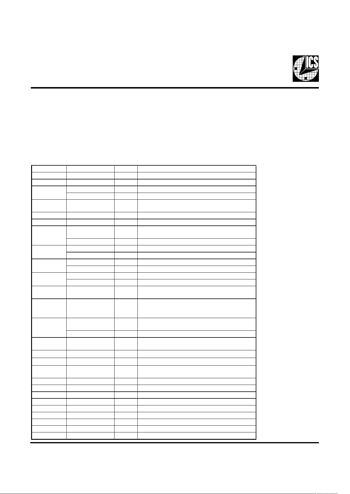
Pin Descriptions
Pi n n umber Pi n n ame Type Desc ription
1, 7, 13, 19, 25, 31 GND PWR Ground pins
2 REF0 OUT 14.318MHz reference clock outputs at 3.3V
REF1 OUT 14.318MHz reference clock outputs at 3.3V
SEL24_48 IN Logic input to select 24 or 48MHz for pin 26 output
4, 10, 16, 23,
28, 35
VDD PWR Power pins 3.3V
5 X1 IN XTAL_IN 14.318MHz crystal input
6 X2 OUT XTAL _OUT C rystal output
PCICLK_F OUT
Free running PC I c l oc k at 3.3V. Sync hro nous to C PU cl ocks. Not
affected b
y
the PCI_STOP# i nput.
FS0 IN Logi c - input for frequency se l ection
PCICLK 1 OUT PCI clock output at 3.3V. Synch ronous to C PU c l ocks.
FS1 IN Logi c - input for frequency se l ection
PCICLK 2 OUT PCI clock output at 3.3V. Synch ronous to C PU c l ocks.
FS2 IN Logi c - input for frequency se l ection
PCICLK 3 OUT PCI clock output at 3.3V. Synch ronous to C PU c l ocks.
FS3 IN Logi c - input for frequency se l ection
14, 15, 17, 18 , 2 0 ,
21, 22
PCICLK [4:10] OUT PCI clock outputs at 3.3V. Synchronous to CPU clocks.
24 PD# IN
This asynchronous input powers down the chip when drive
active(Low). The internal PLLs are disabled and all the output clocks
are held at a Low state.
24_48MHz OUT
24 or 48MHz ou tp ut sel ectable by
SEL24_48# (0=48MHz 1=24MHz)
FRE Q_ A PIC IN L o g i c input for fre q u ency sele ction of IOA PIC
27 48MHz/SEL_3V66 OUT/IN
Fixed 48MHz clock output. 3.3V / Logic input to select the
fre
q
uency of the 3V66 ou tputs
29 SCLK IN
Clock in
p
ut of I2C inpu
t
30 SDATA IN
Data in
p
ut for I2C serial input.
32, 33, 34 3V66[0:2] OUT
3.3V clock outputs. These outputs are stopped when CPU_STOP#
is driven active..
36 GNDLCPU PWR Ground pin for the CPUCLKs
37, 38, 40 CPUCLK[0:2] OUT Host bus clock output at 2.5V.
39 VDDLCPU PWR Power pin for the CPUCLKs. 2.5V
41 GNDLCPU/2 PWR Ground pin for the CPU/2 clocks.
42 CPU/2 OUT 2.5V clock outputs at 1/2 CPU frequency.
43 VDDL C PU/2 PWR Power pin for the CPU/2 clocks. 2.5V
45 GNDLIOAPIC PWR Ground pin for the IOAPIC outputs.
44, 46, 47 IOAPIC[0:2] OUT IOAPIC clocks at 2.5V. Synchronous with CPUCLKs
48 VDDLIOAPIC PWR Power pin for the IOAPIC outputs. 2.5V.
12
26
3
8
9
11
Power Groups:
VDDREF, GNDREF = REF, X1, X2
GNDPCI, VDDPCI = PCICLK
VDD66, GND66 = 3V66
VDD48, GND48 = 48MHz
VDDCOR, GNDCOR = PLL Core
VDDLCPU/2 , GNDLCPU/2 = CPU/2
VDDLIOAPIC, GNDIOAPIC = IOAPIC
Page 3
3
ICS9248-77
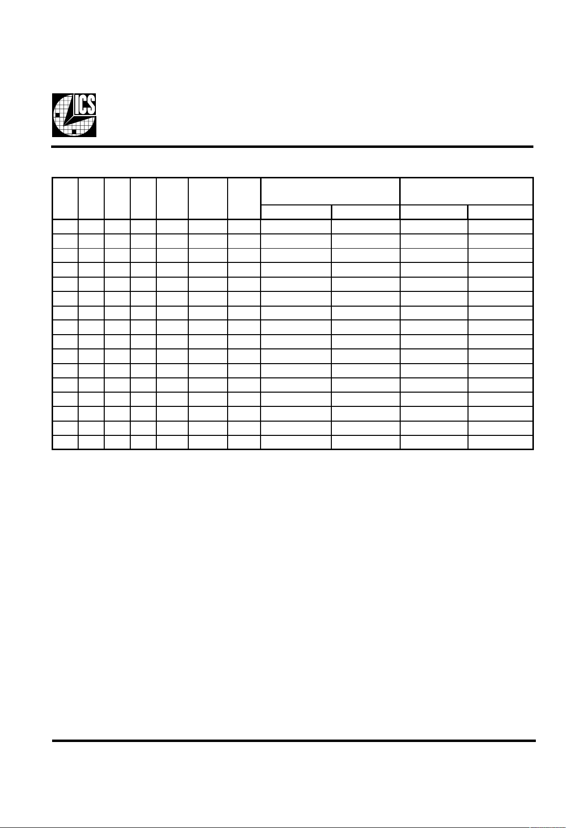
Note:
* These output frequencies are Not synchronous to CPUCLK and Do Not have Spread Spectrum modulation.
Frequency Selection
3SF2SF1SF0SF
UPC
zHM
2/UPC
zHM
ICP
zHM
zHM66V3zHMCIPAOI
0=66V3_LES1=66V3_LES0=CIPA_QERF1=ICPA_QERF
0000 5015.255307075.7153
0001 575.735.73*465757.815.73
0010 3.00151.054.336.666.667.614.33
0011 8.664.334.336.666.6676.614.33
0100 011556.63*463.373.816.63
0101 5115.753.83*466.6761.913.83
0110 7115.8593*46875.9193
0111 0210604*46080204
1000 5215.266.14*463.388.026.14
100 1 7215.363.24*466.4861.123.24
10 10 3.3315.663.336.666.666.613.33
10 11 5315.7657.335.765.768.6157.33
1100 7315.8652.435.865.86521.7152.43
1101 041075307075.7153
1110 5415.2752.63*465.27521.8152.63
1111 051575.73*465757.815.73
Page 4
4
ICS9248-77
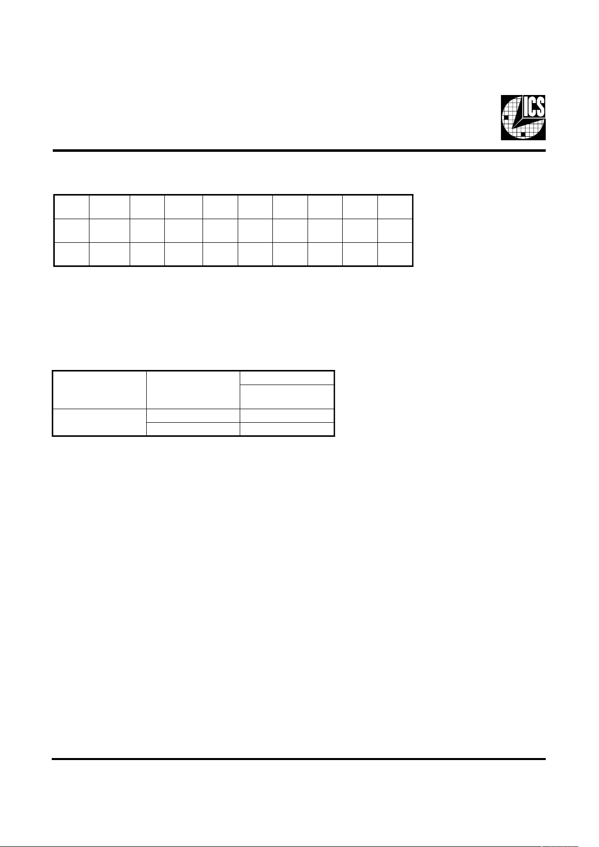
Power Management Features:
Note:
1. LOW means outputs held static LOW as per latency requirement next page.
2. On means active.
3. PD# pulled Low, impacts all outputs including REF and 48 MHz outputs.
#DPKLCUPC2/UPCCIPAOI66V3ICPF_ICP
.FER
zHM84
csOsOCV
0WOLWOLWOLWOLWOLWOLWOLFFOFFO
1NONONONONONONONONO
Power Management Requirements:
Note:
1. Clock on/off latency is defined in the number of rising edges of free running PCICLKs between the clock disable goes low/
high to the first valid clock comes out of the device.
2. Power up latency is when PWR_DWN# goes inactive (high to when the first valid clocks are dirven from the device.
langiSetatSlangiS
ycnetaL
fosegdegnisirfo.oN
KLCICP
#DP
)noitarepolamron(1Sm3
)nwodrewop(0.xam2
Page 5
5
ICS9248-77
1. The ICS clock generator is a slave/receiver, I2C component. It can read back the data stored in the latches for verification.
Read-Back will support Intel PIIX4 "Block-Read" protocol.
2. The data transfer rate supported by this clock generator is 100K bits/sec or less (standard mode)
3. The input is operating at 3.3V logic levels.
4. The data byte format is 8 bit bytes.
5. To simplify the clock generator I2C interface, the protocol is set to use only "Block-Writes" from the controller. The
bytes must be accessed in sequential order from lowest to highest byte with the ability to stop after any complete byte
has been transferred. The Command code and Byte count shown above must be sent, but the data is ignored for those
two bytes. The data is loaded until a Stop sequence is issued.
6. At power-on, all registers are set to a default condition, as shown.
General I2C serial interface information
The information in this section assumes familiarity with I2C programming.
For more information, contact ICS for an I2C programming application note.
How to Write:
Controller (host) sends a start bit.
Controller (host) sends the write address D2
(H)
ICS clock will acknowledge
Controller (host) sends a dummy command code
ICS clock will acknowledge
Controller (host) sends a dummy byte count
ICS clock will acknowledge
Controller (host) starts sending first byte (Byte 0)
through byte 5
ICS clock will acknowledge each byte one at a time.
Controller (host) sends a Stop bit
How to Read:
Controller (host) will send start bit.
Controller (host) sends the read address D3
(H)
ICS clock will acknowledge
ICS clock will send the byte count
Controller (host) acknowledges
ICS clock sends first byte (Byte 0) through byte 5
Controller (host) will need to acknowledge each byte
Controller (host) will send a stop bit
Notes:
Controller (Host) ICS (Slave/Receiver)
Start Bit
Address
D3
(H)
AC
K
Byte Count
ACK
Byte
0
ACK
Byte 1
ACK
Byte
2
ACK
Byte
3
ACK
Byte 4
ACK
Byte
5
ACK
Stop Bit
How to Read:
Controller (Host) ICS (Slave/Receiver)
Start Bit
Address
D2
(H)
AC
K
Dummy Command Code
AC
K
Dummy Byte Count
AC
K
Byte 0
AC
K
Byte 1
AC
K
Byte 2
ACK
Byte 3
AC
K
Byte 4
AC
K
Byte 5
AC
K
Stop Bit
How to Write:
Page 6

6
ICS9248-77
Byte 0: Functionality and frequency select register (Default = 0)
Serial Configuration Command Bitmap
Note 1: Default at power-up will be for latched logic inputs to define frequency.
* These output frequencies are not synchronous to CPUCLK and do not have Spread Spectrum modulation.
tiBnoitpircseDDWP
7tiB
murtcepSdaerpSretneC%52.0±-0
0
%5.-ot0murtcepSdaerpSnwoD-1
tiB
)4:6,2(
)4:6,2(tiBKLCUPC
66V3
KLCICP
CIPAOI
1etoN
0=LES_66V31=LES_66V30=CIPA_QERF1=CIPA_QERF
00005010707535.7153
100057*46575.7357.815.73
01003.0016.666.664.337.614.33
11008.666.666.664.3376.614.33
0010011*463.376.633.816.63
1010511*466.673.8361.913.83
0110711*4687935.9193
1110021*4608040204
0001521*463.386.148.026.14
1001721*466.483.2461.123.24
01013.3316.666.663.336.613.33
11015315.765.7657.338.6157.33
00117315.865.8652.43521.7152.43
10110410707535.7153
0111541*465.2752.63521.8152.63
1111051*46575.7357.815.73
3tiB
stupnidehctal,tceleserawdrahybdetcelessiycneuqerF-0
4:6,2tiBybdetcelessiycneuqerF-1
0
1tiB
lamroN-0
delbanemurtcepsdaerpS-1
0
0tiB
gninnuR-0
stuptuollaetatsirT-1
0
Page 7

7
ICS9248-77
Byte 1: CPU, Active/Inactive Register
(1 = enable, 0 = disable)
Byte 2: PCI Active/Inactive Register
(1 = enable, 0 = disable)
Byte 3: 3V66 Active/Inactive Register (1 =
enable, 0 = disable)
Note:
1. Inactive means outputs are held LOW and are disabled
from switching.
Notef:
1. Inactive means outputs are held LOW and are disabled
from switching.
Note:
1. Inactive means outputs are held LOW and are disabled
from switching.
Byte 4: PCI Active/Inactive Register (1 =
enable, 0 = disable)
Note:
1. Inactive means outputs are held LOW and are disabled
from switching.
tiB#niPDWPnoitpircseD
7tiB041 0KLCUPC
6tiB831 1KLCUPC
5tiB731 2KLCUPC
4tiB241 2/UPC
3tiB741 0CIPAOI
2tiB641 1CIPAOI
1tiB21 1FER
0tiB31 0FER
tiB#niPDWPnoitpircseD
7tiB811 7KLCICP
6tiB711 6KLCICP
5tiB511 5KLCICP
4tiB411 4KLCICP
3tiB211 3KLCICP
2tiB111 2KLCICP
1tiB91 1KLCICP
0tiB81 F_KLCICP
tiB#niPDWPnoitpircseD
7tiB431 0_66V3
6tiB331 1_66V3
5tiB231 2_66V3
4tiB-X#1SF
3tiB-1 )devreseR(
2tiB-1 )devreseR(
1tiB-X#3SF
0tiB-X#2SF
tiB#niPDWPnoitpircseD
7tiB621 zHM84_42
6tiB721 zHM84
5tiB-X0SF
4tiB221 01KLCICP
3tiB121 9KLCICP
2tiB021 8KLCICP
1tiB-1 )devreseR(
0tiB-1 )devreseR(
Byte 5: Active/Inactive Register
(1= enable, 0 = disable)
Note: Dont write into this register, writing into this register
can cause malfunction
tiB#niPDWPnoitpircseD
7tiB-0 )etoN(devreseR
6tiB-0 )etoN(devreseR
5tiB-0 )etoN(devreseR
4tiB-0 )etoN(devreseR
3tiB-0 )etoN(devreseR
2tiB-1 )etoN(devreseR
1tiB-1 )etoN(devreseR
0tiB-0 )etoN(devreseR
Page 8

8
ICS9248-77
PD# Timing Diagram
The power down selection is used to put the part into a very low power state without turning off the power to the part. PD# is
an asynchronous active low input. This signal needs to be synchronized internal to the device prior to powering down the clock
synthesizer.
Internal clocks are not running after the device is put in power down. When PD# is active low all clocks need to be driven to a
low value and held prior to turning off the VCOs and crystal. The power up latency needs to be less than 3 mS. The power down
latency should be as short as possible but conforming to the sequence requirements shown below. The REF and 48MHz clocks
are expected to be stopped in the LOW state as soon as possible. Due to the state of the internal logic, stopping and holding
the REF clock outputs in the LOW state may require more than one clock cycle to complete.
Notes:
1. All timing is referenced to the Internal CPUCLK (defined as inside the ICS9248 device).
2. As shown, the outputs Stop Low on the next falling edge after PD# goes low.
3. PD# is an asynchronous input and metastable conditions may exist. This signal is synchronized inside this part.
4. The shaded sections on the VCO and the Crystal signals indicate an active clock.
5. Diagrams shown with respect to 133MHz. Similar operation when CPU is 100MHz.
Page 9

9
ICS9248-77
Absolute Maximum Ratings
Supply Voltage . . . . . . . . . . . . . . . . . . . . . . . . . . . 7.0 V
Logic Inputs . . . . . . . . . . . . . . . . . . . . . . . . . . . . GND 0.5 V to VDD +0.5 V
Ambient Operating Temperature . . . . . . . . . . . . 0°C to +70°C
Storage Temperature . . . . . . . . . . . . . . . . . . . . . . 65°C to +150°C
Case Temperature . . . . . . . . . . . . . . . . . . . . . . . . 115°C
Stresses above those listed under Absolute Maximum Ratings may cause permanent damage to the device. These ratings are
stress specifications only and functional operation of the device at these or any other conditions above those listed in the
operational sections of the specifications is not implied. Exposure to absolute maximum rating conditions for extended periods
may affect product reliability.
Electrical Characteristics - I nput/Suppl y/Common Output Paramet ers
TA = 0 - 70º C; V
DD, VDDL
= 3.3 V +/- 5% (unless otherwise stated)
PARAMETER
SYMBOL CONDITIONS MIN TYP MAX UNITS
Input High Voltage
V
IH
2V
DD
+0.3 V
Input Low Voltage
V
IL
VSS-0.3 0.8 V
Inpu t High Current
I
IH
VIN = V
DD
0.1 5
µ
A
Input L ow Current
I
IL1
VIN = 0 V; Input s wit h no pu l l-up resisto rs -5 2.0
µ
A
Input L ow Current
I
IL2
VIN = 0 V; Inputs with pul l-up resistors -20 0 -1 00
µ
A
I
DD3.3OP100CL
= 0 pF; Select @ 100 MHz
81 160 mA
I
DD3.3OP133CL
= 0 pF; Select @ 133 MHz
85 160 mA
Input frequency
F
i
VDD = 3 .3 V; 11 14.318 16 MHz
C
IN
Logic Inputs 5 pF
C
INX
X 1 & X2 pins 27 36 45 pF
Tr ansition Time
1
T
trans
To 1st cros sing of target Freq. 3 ms
Settling Time
1
T
s
From 1st crossing to 1% t arget Fre q. 5 3 ms
Clk Stabiliza tion
1
T
STAB
From VDD = 3.3 V to 1% t a rget F req.
3ms
1
G ua rantee d by de sign, not 100% teste d i n production.
Input Capacita nce
1
Operating Supply
Current
Electrical Characteristics - I nput/Supply/Comm on Output Parameters
TA = 0 - 70º C; VDD = 3.3 V +/-5%; V
DDL
= 2.5 V +/- 5% (unless otherwise stated)
PARAMETER SYMBOL CONDITIONS MIN TYP MAX UNITS
Operating I
DD2.5OP 100CL
= 0 pF; Select @ 100 MHz 16 75 m A
Supply Current I
DD2.5OP 133CL
= 0 pF; Select @ 133 MHz 19 90 m A
Power Down Supply Current
I
DD2.5P D
CL = 0 pF; PWRD WN# = 0
0.1 100 µA
1
Guaranteed by desi g n, not 100% tested in pr od uc t ion.
Page 10

10
ICS9248-77
Ele ctrical C haracteristics - CPUCLK
TA = 0 - 70º C; VDD = 3.3 V +/-5%, V
DDL
= 2.5 V +/-5%; CL = 20 pF (unless othe rw ise stated)
PARAMETER SYMBOL CONDITIONS MIN TYP MAX UNITS
Output High Voltage V
OH2B
IOH = -12.0 mA 2 2.24 V
Output Low Voltage V
OL2B
IOL = 12.0 mA 0.31 0.4 V
O utput High Cur rent I
OH2B
VOH = 1 .7 V -31 -19 mA
Ou tput Low Cu rrent I
OL2B
VOL = 0.7 V 19 25 mA
Rise Time t
r2B
1
VOL = 0.4 V, VOH = 2.0 V 1.35 1.6 ns
Fall Time t
f2B
1
VOH = 2.0 V, VOL = 0 .4 V 1.4 1.6 ns
Duty Cycle d
t2B
1
VT = 1.25 V 454755%
Skew t
sk2B
1
VT = 1.25 V 63 175 ps
Jitter, Cycle-to-cycle t
jcyc-cyc2B
1
VT = 1.25 V 125 250 ps
Jitter, O ne Sigma t
j1s2B
1
VT = 1.25 V 65 150 ps
Jitter, A bsolute
t
jabs2B
1
VT = 1.25 V
-250 148 +250 ps
1
G ua rantee d by d e sign, not 100% teste d i n production.
Ele ctrical C haracteristics - CP U/ 2
TA = 0 - 70º C; VDD = 3.3 V +/-5%, V
DDL
= 2.5 V +/-5%; CL = 20 pF (unless othe rw ise stated)
PARAMETER SYMBOL CONDITIONS MIN TYP MAX UNITS
Output High Voltage V
OH2B
IOH = -12.0 mA 2 2.24 V
Output Low Voltage V
OL2B
IOL = 12.0 mA 0.31 0.4 V
O utput High Cur rent I
OH2B
VOH = 1 .7 V -31 -19 mA
Ou tput Low Cu rrent I
OL2B
VOL = 0.7 V 19 26 mA
Rise Time t
r2B
1
VOL = 0.4 V, VOH = 2 .0 V 1.2 1.6 ns
Fall Time t
f2B
1
VOH = 2.0 V, VOL = 0 .4 V 1.2 1.6 ns
Duty Cycle d
t2B
1
VT = 1.25 V 454955%
Jitter, Cycle-to-cycle t
jcyc-cyc2B
1
VT = 1.25 V 125 250 ps
Jitter, O ne Sigma t
j1s2B
1
VT = 1.25 V 50 150 ps
Jitter, A bsolute
t
jabs2B
1
VT = 1.25 V
-250 97 +250 ps
1
G ua rantee d by d e sign, not 100% teste d i n production.
Group Of fset
Group Offset Measurement Loads Measure Points
CPU to 3V66 0.0-1.5ns CPU leads CPU @ 20pF, 3V66 @ 30pF CPU @1.25V, 3V66 @ 1.5V
3V66 to PCI 1.5-4.0ns 3V66 leads 3V66 @ 30pF, PCI @ 30pF 3V66 @ 1.5V, PCI @ 1.5V
CPU to IOAPIC 1.5-4.0ns CPU leads CPU @ 20pF, IOAPIC @ 20pF CPU @1.25V, IOAPIC @ 1.5V
N ot e: 1. All of fsets are to be measured at rising edges.
Page 11

11
ICS9248-77
Electrical Characteristics - PCICLK
TA = 0 - 70º C; VDD = 3.3 V +/-5%, V
DDL
= 2.5 V +/-5%; CL = 30 pF (unless otherwise stated)
PARAMETER SYMBO
L
CONDITIONS MIN TYP MAX UNITS
Output High Voltage V
OH1
I
O
H
= -11 mA 2.4 3.1 V
Output Low Voltage V
OL1
I
O
L
= 9.4 mA 0.16 0.4 V
Output High Current I
OH1
V
O
H
= 2.0 V -50 -22 mA
Output Low Current I
OL1
V
O
L
= 0.8 V 16 42 mA
Rise Time
1
t
r1
V
O
L
= 0.4 V, V
O
H
= 2.4 V 2 2 ns
Fall Time
1
t
f1
V
O
H
= 2.4 V, V
O
L
= 0.4 V 1.74 2 ns
Duty Cycle
1
d
t1
VT = 1.5 V 45 49 55 %
Skew
1
t
sk1
VT = 1.5 V 290 500 ps
Jitter, Cycle-to-cycle
1
T
jcy
c-cyc1
VT = 1.5 V 290 500 ps
Jitter, One Sigma
1
t
j
1s1
VT = 1.5 V 30 150 ps
Jitter, Absolute
1
t
jabs1
VT = 1.5 V
-250 121 250 ps
1
Guarant eed by design, not 100% tested in production.
Electrical Characteristics - 3V66
TA = 0 - 70º C; VDD = 3.3 V +/-5%, V
DDL
= 2.5 V +/-5%; CL = 30 pF (unless otherwise stated)
PARAMETER SYMBOL CONDITIONS MIN TYP MAX UNITS
Output High Voltage V
OH1
IOH = -11 mA 2.4 3.1 V
Output Low Voltage V
OL1
IOL = 9.4 mA 0.17 0.4 V
Output High Current I
OH1
VOH = 2.0 V -51 -22 mA
Output Low Current I
OL1
VOL = 0.8 V 16 41 mA
Rise Time
1
t
r1
VOL = 0.4 V, VOH = 2.4 V 0.5 1.8 2 ns
Fall Time
1
t
f1
VOH = 2.4 V, VOL = 0.4 V 0.5 1.6 2 ns
Duty Cycle
1
d
t1
VT = 1.5 V 45 49 55 %
Skew
1
t
sk1
VT = 1.5 V 50 250 ps
Jitter, Cycle-to-cycle
1
T
jcy
c-cyc1
VT = 1.5 V 299 500 ps
Jitter, One Sigma
1
t
j
1s1
VT = 1.5 V 87 150 ps
Jitter, Absolute
1
t
jabs1
VT = 1.5 V
-500 235 500 ps
1
Guaranteed by design, not 100% tested in production.
Page 12

12
ICS9248-77
Electrical Characteristics - 48 MHz
TA = 0 - 70ºC; VDD = 3.3 V +/-5%; V
DDL
= 2.5 V +/-5%; CL = 20 pF (unless otherwise stated)
PARAMETER SYMBOL CONDITIONS MIN TYP MAX UNITS
Output High Voltage V
OH5
IOH = -16 mA 2.4 2.62 V
Output Low Voltage V
OL5
IOL = 9 mA 0.3 0.4 V
Output High Curre nt I
OH5
VOH = 2.0 V -27 -22 mA
Output Low Current I
OL5
VOL = 0.8 V 16 22 mA
Rise Time
1
t
r5
VOL = 0.4 V, VOH = 2.4 V 2.1 4 ns
Fall Time
1
t
f5
VOH = 2.4 V, VOL = 0.4 V 2.2 4 ns
Duty Cycle
1
d
t5
VT = 1.5 V 45 51 55 %
Jitter, Cycle-to-cycle
1
T
jcy
c-cyc5
VT = 1.5 V 488 500 ps
Jitter, One Sigma
1
t
j
1s5
VT = 1.5 V 0.29 3 %
Jitter, Absolute
1
t
jabs5
VT = 1.5 V
-5 1.05 5 %
1
Guaranteed by design, not 100% tested in production.
Electrical Characteristics - REF
TA = 0 - 70ºC; VDD = 3.3 V +/-5%, V
DDL
= 2.5 V +/-5%; CL = 20 pF (unless otherwise stated)
PARAMETER SYMBOL CONDITIONS MIN TYP MAX UNITS
Output High Voltage V
OH5
IOH = -16 mA 2.4 2.6 V
Output Low Voltage V
OL5
IOL = 9 mA 0.3 0.4 V
Output High Curre nt I
OH5
VOH = 2.0 V -26 -22 mA
Output Low Current I
OL5
VOL = 0.8 V 16 22 mA
Rise Time
1
t
r5
VOL = 0.4 V, VOH = 2.4 V 2.2 4 ns
Fall Time
1
t
f5
VOH = 2.4 V, VOL = 0.4 V 2.2 4 ns
Duty Cycle
1
d
t5
VT = 1.5 V 45 52 55 %
Jitter, Cycle-to-cycle
1
T
jcy
c-cyc5
VT = 1.5 V 600 1000 ps
Jitter, One Sigma
1
t
j
1s5
VT = 1.5 V 0.44 3 %
Jitter, Absolute
1
t
jabs5
VT = 1.5 V
-5 0.94 5 %
1
Guaranteed by design, not 100% tested in production.
Page 13

13
ICS9248-77
Electrical Characteristics - IOAPIC
TA = 0 - 70º C; VDD = 3.3 V +/-5%, V
DDL
= 2.5 V +/-5%; CL = 20 pF (unless otherwise stated)
PARAMETER SYMBOL CONDITIONS MIN TYP MAX UNITS
Output High Voltage V
OH4B
IOH = -12.0 mA 2 2.24 V
Output Low Voltage V
OL4B
IOL = 12.0 mA 0.31 0.4 V
Output High Curre nt I
OH4B
VOH = 1.7 V -31 -19 mA
Output Low Current I
OL4B
VOL = 0.7 V 19 26 mA
Rise Time
1
T
r4B
VOL = 0.4 V, VOH = 2.0 V 1.46 2 ns
Fall Time
1
T
f4B
VOH = 2.0 V, VOL = 0.4 V 1.44 2 ns
Duty Cycle
1
D
t4B
VT = 1.25 V 45 49 55 %
Skew
1
t
sk4B
VT = 1.25 V 139 250 ps
Jitter, Cycle-to-cycle
1
T
jcy
c-cyc4BVT
= 1.25 V 167 500 ps
Jitter, One Sigma
1
T
j
1s4B
VT = 1.25 V 30 150
ps
Jitter, Absolute
1
T
jabs4B
VT = 1.25 V
-250 104 250
ps
1
Guaranteed by design, not 100% tested in production.
Page 14

14
ICS9248-77
SSOP Package
ICS reserves the right to make changes in the device data identified in
this publication without further notice. ICS advises its customers to
obtain the latest version of all device data to verify that any
information being relied upon by the customer is current and accurate.
LOBMYS SNOISNEMIDNOMMOC SNOITAIRAV D N
.NIM.MON.XAM.NIM.MON.XAM
A590.101.011.CA026.526.036.84
1A800.210.610.
2A880.090.290.
B800.010.5310.
C500.- 010.
DsnoitairaVeeS
E292.692.992.
eCSB520.0
H004.604.014.
h010.310.610.
L420.230.040.
NsnoitairaVeeS
µ
°0 °5 °8
X580.390.001.
Ordering Information
ICS9248yF-77
Pattern Number (2 or 3 digit number for parts with ROM code patterns)
Package Type
F=SSOP
Revision Designator
Device Type (consists of 3 or 4 digit numbers)
Prefix
ICS, AV = Standard Device
Example:
ICS XXXX y F - PPP
 Loading...