

Page 1
Integrated
Circuit
Systems, Inc.
General Description Features
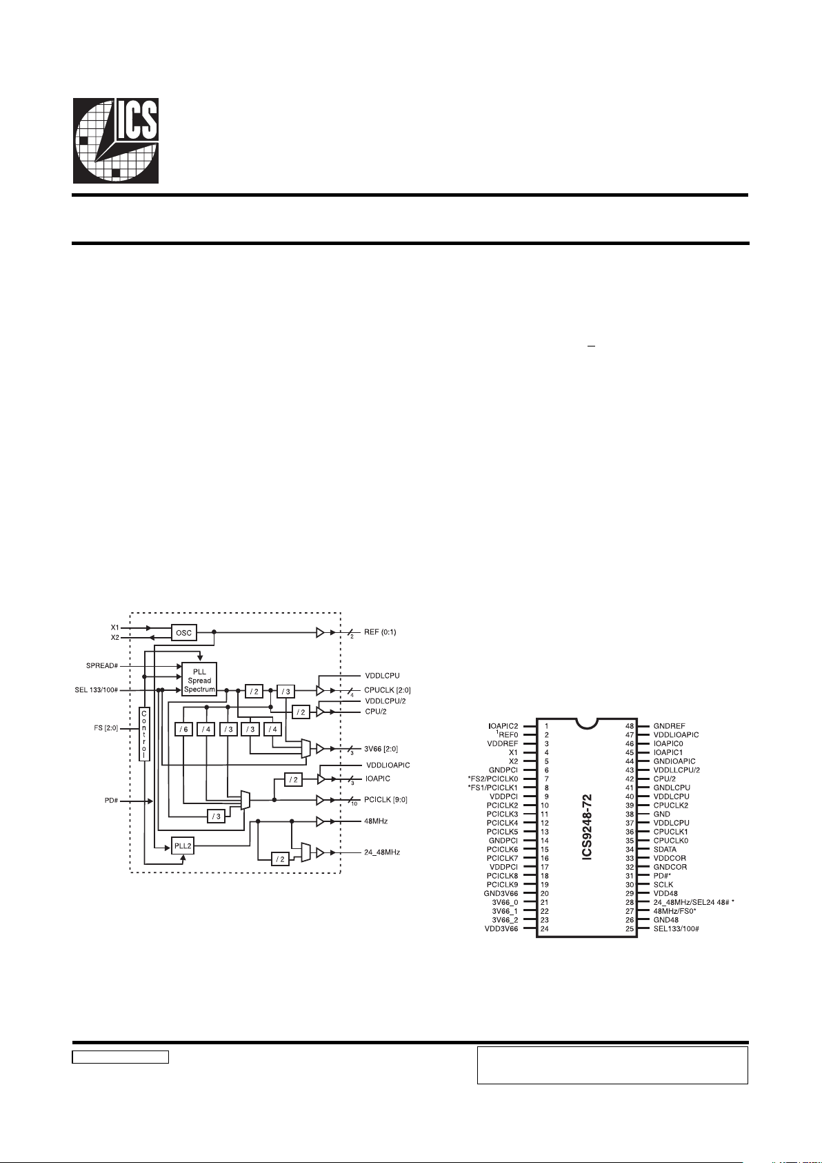
ICS9248-72
Block Diagram
Frequency Timing Generator for PENTIUM II Systems
9248-72 Rev B 7/28/99
Pin Configuration
48-pin SSOP
Up to 200MHz frequency support.
Power Down feature.
Spread Spectrum for EMI control
(0 to 0.5% down spread , + 0.25% center spread)
I2C interface.
VDDL=2.5V,VDD=3.3V
The ICS9248-72 is a main clock synthesizer chip for Pentium
II based systems using Rambus Interface DRAMs. This chip
provides all the clocks required for such a system when used
with a Direct Rambus Clock Generator(DRCG) chip such as
the ICS9211-01.
Spread Spectrum may be enabled by driving the SPREAD#
pin active. Spread spectrum typically reduces system EMI by
8dB to 10dB. This simplifies EMI qualification without resorting
to board design iterations or costly shielding. The ICS9248-
72 employs a proprietary closed loop design, which tightly
controls the percentage of spreading over process and
temperature variations.
The CPU/2 clocks are inputs to the DRCG.
Preliminary Product Preview
* 250K ohm pull-up to VDD on indicated inputs.
1.These pins will have 2X drive strength
Key Specification
CPU Output Jitter: <250ps
CPU/2 Output Jitter. <250ps
IOAPIC Output Jitter: <500ps
48MHz, 3V66, PCI Output Jitter: <500ps
Ref Output Jitter. <1000ps
CPU Output Skew: <175ps
IOAPIC Output Skew <250ps
PCI Output Skew: <500ps
3V66 Output Skew <250ps
CPU to 3V66 Output Offset: 0.0 - 1.5ns (CPU leads)
3V66 to PCI Output Offset: 1.5 - 4.0ns (3V66 leads)
CPU to IOAPIC Output Offset 1.5 - 4.0ns (CPU leads)
PRODUCT PREVIEW documents contain information on new
products in the sampling or preproduction phase of development.
Characteristic data and other specifications are subject to change
without notice.
Page 2
2
ICS9248-72
Preliminary Product Preview
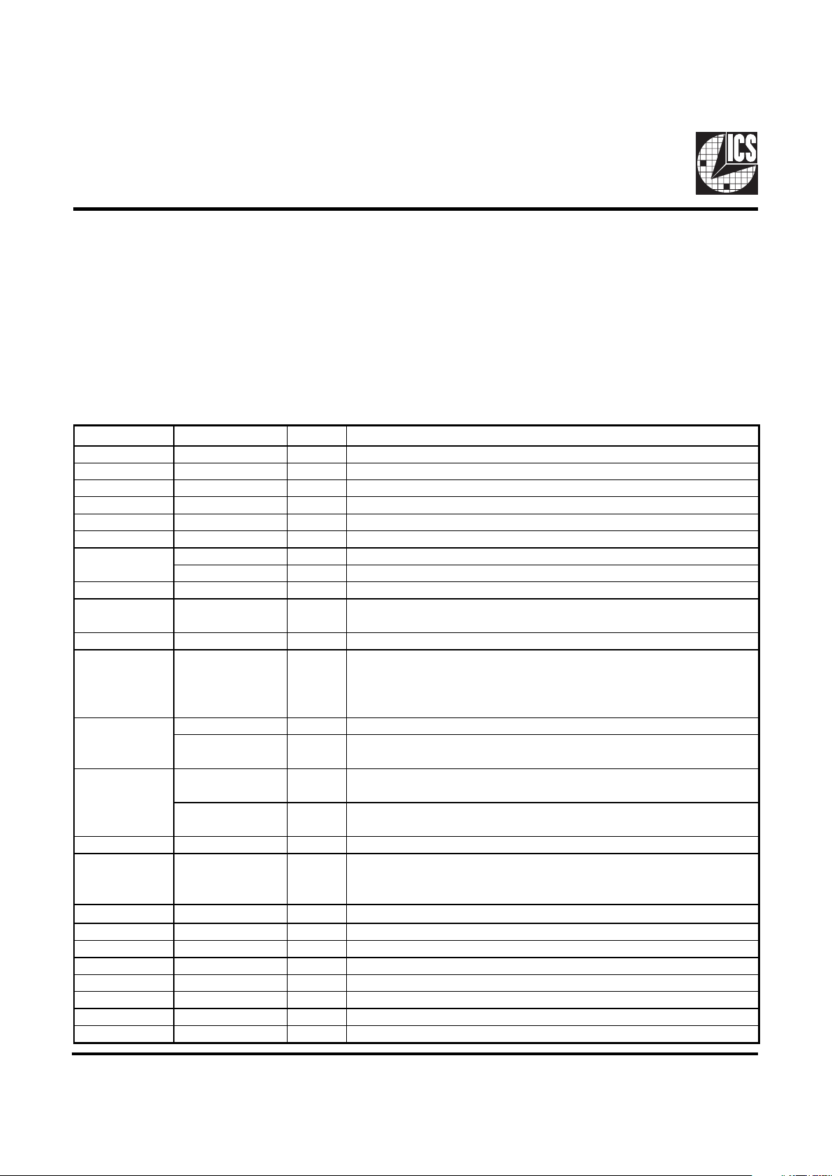
Pin Descriptions
Pin number Pin name Type Description
1, 45, 46 IOA P I C [ 2:0] O utput 2.5V IO AP I C clock ou tputs
2 REF0 O utput 3.3V, 14.318 M Hz re f e r enc e c lock output.
3, 24, 29, 33 VDD Power 3.3 V powe r
4 X 1 Input 14.318 M Hz cry sta l input
5 X 2 O utput 14.318 M Hz cry sta l output
6, 14, 20, 26, 32 GN D P ower G r ound
FS [2:1] IN Fr e quenc y s elect p ins. L atc hed I nputs de ter mins the CP U & P C I f r e quenc ies .
PC I C L K [1:0] O utput 3.3 V PCI clock outputs, ge ne r ating tim ing r equir e ments f or
9,17 VDD PCI Power 3.3 V powe r for the P C I cloc k outputs
19, 18, 16, 15, 13,
12, 11, 10
PC I C L K [9:2] O utput 3.3 V PCI clock outputs
23, 22, 21 3V 66 Outpu t 3.3 V 66 MH z c lock output, f ixe d f r e quenc y cloc k typically us ed with A GP
25 SE L 133/100# Input
control f or the f r eq uency of clocks a t the CPU output pins . I f logic "0" is us ed the
100 MHz fr eq uenc y is s e lecte d. I f L og ic " 1" is used, the 133 M Hz fr e quenc y is
selec ted. T he PCI c lock is multiplexed to run at 33. 3 M Hz for both selected c as e s.
FS0
IN Fr e quenc y s elect p in. L a tched Inputs deter mins the CP U & P C I frequenc ies .
48 MHz O utput
3.3 V 48 MH z clock outpu t, fixed fr eq uenc y clock typic ally us ed with U S B
devices
SEL24/48
IN
48/24 MHz sel ect option. Active low = 48 MHz output. Active High = 24
MHz
24_48MHz#
Output
3.3V 48 or 24 MHz clock output, fixed frequency clock typi cally us ed wi th
USB devices.
30 SC L K I N Clock input of I 2C input
31 PD # Input
As ync hr onous a ctive low input pin used to pow er down the device into a low
power state. The internal clocks are disabled and the VCO and the crystal are
stopped.
34 SDATA IN
D ata in put for I
2
C se r ial input.
36, 35 C P UCL K [1:0] 0 utput 2.5 V CP U and H os t cloc k outputs
37, 40 VDDLCPU Power 2.5 V power for the CPU and Host clock outputs
41 GNDLCPU/2 Power Ground for the CPU a nd Host clock outputs
42 CP U/2 O utput output running at 1/2 C P U clock f r e quenc y. S ync hr onous to the CPU outputs .
43 VDDLCPU/2 Power 2.5 V powe r for the CPU/2 c lock outputs
47 GNDLI OA P IC Pow er Ground f or IOAPIC c locks
48 G NDR E F Power Ground for 14. 318 M Hz re ference cloc k outputs
8, 7
28
27
Power Groups:
VDDREF, GNDREF = REF, X1, X2
GNDPCI, VDDPCI = PCICLK
VDD66, GND66 = 3V66
VDD48, GND48 = 48MHz
VDDCOR, GNDCOR = PLL Core
VDDLCPU/2 , GNDLCPU/2 = CPU/2
VDDLIOAPIC, GNDIOAPIC = IOAPIC
Page 3
3
ICS9248-72
Preliminary Product Preview
ICS9248-72 Power Management Features:
Note:
1. LOW means outputs held static LOW as per latency requirement next page.
2. On means active.
3. PD# pulled Low, impacts all outputs including REF and 48 MHz outputs.
#DPKLCUPC2/UPCCIPAOI66V3ICPF_ICP
.FER
zHM84
csOsOCV
0WOLWOLWOLWOLWOLWOLWOLFFOFFO
1NONONONONONONONONO
Power Management Requirements:
Note:
1. Clock on/off latency is defined in the number of rising edges of free running PCICLKs between the clock disable goes low/
high to the first valid clock comes out of the device.
2. Power up latency is when PWR_DWN# goes inactive (high to when the first valid clocks are dirven from the device.
lagniSetatSlagniS
ycnetaL
segdegnisirfo.oN
KLCICPfo
#DP
)noitarepolamron(1Sm3
)nwodrewop(0.xam2
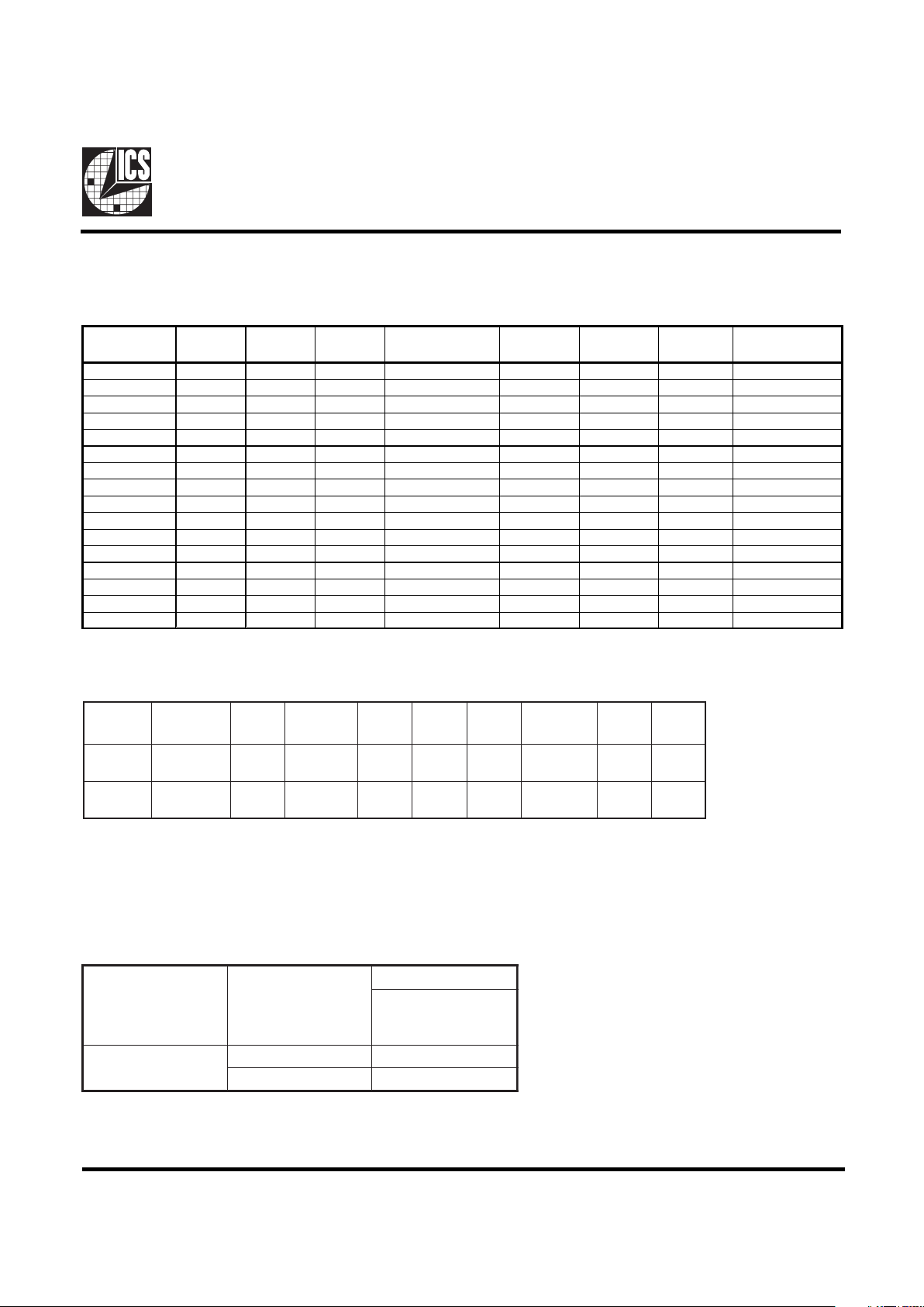
Functionality
VDD = 3.3V±5%, V
DDL
= 2.5V ±5% TA= 0 to 70°C
Crystal (X1, X2) = 14.31818MHz
SEL133/100#
FS2
(MHz)
FS1
(MHz)
FS0
(MHz)
CPU
(MHz)
CPU/2
(MHz)
PCI
(MHz)
3V66
(MHz)
IOAPIC
(MHz)
1111
133.30 66.65 33.325 66.65 16.66
1
1
10
138.01 69.01 34.505 69.01 17.25
1
1
01
142.91 71.45 35.725 71.45 17.86
1
10
0
147.95 73.98 36.99 73.98 18.49
1011
152.49 76.24 38.12 76.24 19.06
1010
156.99 78.49 39.245 78.49 19.62
1001
162.02 81.01 40.505 81.01 20.25
1000
180.00 89.99 30.00 60.00 15.00
0111
100.23 50.11 33.405 66.81 16.70
0110
105.00 52.49 35 70.00 17.50
0101
113.99 56.99 37.83 75.66 18.91
0100
120.00 59.99 40.00 80.00 20.00
0011
128.51 64.25 32.125 64.25 16.06
0010
200.01 1 00.00 33.33 66.66 16.66
0001
170.03 85.01 28.33 56.66 14.16
0000
66.82 33.40 33.40 66.80 16.7
Page 4
4
ICS9248-72
Preliminary Product Preview
1. The ICS clock generator is a slave/receiver, I2C component. It can read back the data stored in the latches for verification.
Read-Back will support Intel PIIX4 "Block-Read" protocol.
2. The data transfer rate supported by this clock generator is 100K bits/sec or less (standard mode)
3. The input is operating at 3.3V logic levels.
4. The data byte format is 8 bit bytes.
5. To simplify the clock generator I2C interface, the protocol is set to use only "Block-Writes" from the controller. The
bytes must be accessed in sequential order from lowest to highest byte with the ability to stop after any complete byte
has been transferred. The Command code and Byte count shown above must be sent, but the data is ignored for those
two bytes. The data is loaded until a Stop sequence is issued.
6. At power-on, all registers are set to a default condition, as shown.
General I2C serial interface information
The information in this section assumes familiarity with I2C programming.
For more information, contact ICS for an I2C programming application note.
How to Write:
Controller (host) sends a start bit.
Controller (host) sends the write address D2
(H)
ICS clock will acknowledge
Controller (host) sends a dummy command code
ICS clock will acknowledge
Controller (host) sends a dummy byte count
ICS clock will acknowledge
Controller (host) starts sending first byte (Byte 0)
through byte 5
ICS clock will acknowledge each byte one at a time.
Controller (host) sends a Stop bit
How to Read:
Controller (host) will send start bit.
Controller (host) sends the read address D3
(H)
ICS clock will acknowledge
ICS clock will send the byte count
Controller (host) acknowledges
ICS clock sends first byte (Byte 0) through byte 5
Controller (host) will need to acknowledge each byte
Controller (host) will send a stop bit
Notes:
Controller (Host) ICS (Slave/Receiver)
Start Bit
Address
D3
(H)
AC
K
Byte Coun
t
ACK
Byte
0
ACK
Byte 1
ACK
Byte
2
ACK
Byte
3
ACK
Byte
4
ACK
Byte
5
ACK
Stop Bit
How to Read:
Controller (Host) ICS (Slave/Receiver)
Start Bit
Address
D2
(H)
AC
K
Dummy Command Code
AC
K
Dummy Byte Count
AC
K
Byte 0
AC
K
Byte 1
AC
K
Byte 2
ACK
Byte 3
AC
K
Byte 4
AC
K
Byte 5
AC
K
Stop Bit
How to Write:
Page 5

5
ICS9248-72
Preliminary Product Preview
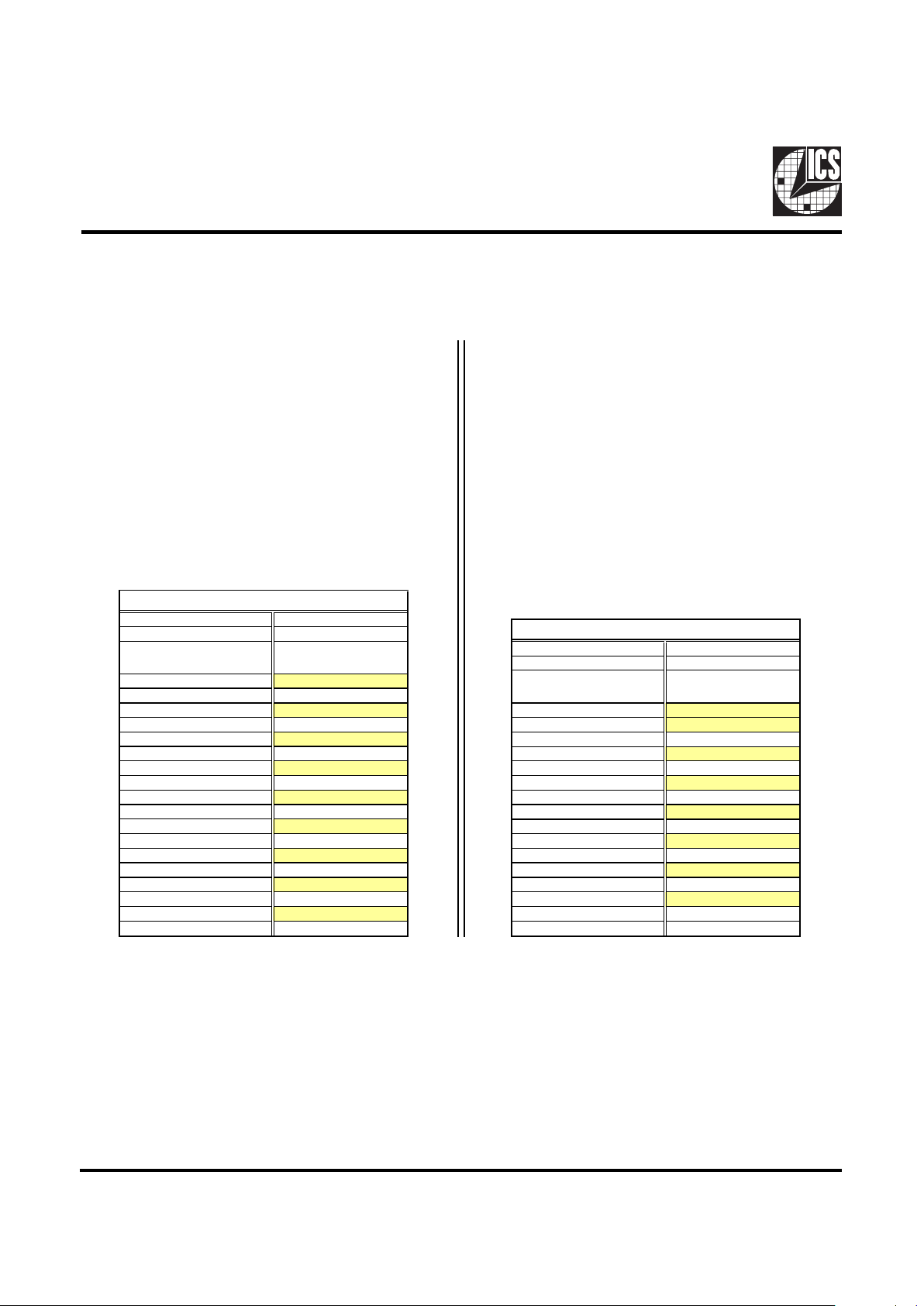
Byte0: Functionality and Frequency Select Register (default = 0)
Serial Configuration Command Bitmap
Note1: Default at power-up will be for latched logic inputs to define frequency.
tiBnoitpircseDDWP
tiB
)4:7(
tiB
KLCUPC2/UPC66V3KLCICPCIPAOI0
7654
1111 03.33156.6656.66523.3366.61
XXXX
1etoN
1110 10.83110.9610.96505.4352.71
1101 19.24154.1754.17527.5368.71
1100 59.74189.3789.3799.6394.81
1011 94.25142.6742.6721.8360.91
1010 99.65194.8794.87542.9326.91
1001 20.26110.1810.18505.0452.02
1000 00.08199.9800.0600.0300.51
0111 32.00111.0518.66504.3307.61
0110 00.50194.2500.075305.71
0101 99.31199.6566.5738.7319.81
0100 00.02199.9500.0800.0400.02
0011 15.82152.4652.46521.2360.61
0010 10.00200.00166.6633.3366.61
0001 30.07110.5866.6533.8261.41
0000 28.6604.3308.6604.337.61
3tiB
stupnidehctal,tceleserawdrahybdetcelessiycneuqerF-0
4:7tiBybdetcelessiycneuqerF-1
0
2tiB
%52.0±epytdaerpsretnecmurtcepsdaerpS-0
%5.0-ot0epytdaerpsnwodmurtcepsdaerpS-1
1
1tiB
lamroN-0
elbanemurtcepsdaerpS-1
1
0tiB
gninnuR=0
stuptuollaetatsirT=1
0
Page 6

6
ICS9248-72
Preliminary Product Preview
Byte 1: CPU, CPU/2, 48MHz Register
(1 = enable, 0 = disable)
Byte 2: PCICLK Active/Inactive Register
(1 = enable, 0 = disable)
Byte 3: 3V66, REF Register Active/Inactive
(1 = enable, 0 = disable)
Notes:
1. Inactive means outputs are held LOW and are disabled
from switching.
Notes:
1. Inactive means outputs are held LOW and are disabled
from switching.
Notes:
1. Inactive means outputs are held LOW and are disabled
from switching.
tiB#niPDWPnoitpircseD
7tiB721 zHM84
6tiB821 zHM84_42
5tiB-- )devreseR(
4tiB2412/UPC
3tiB-- )devreseR(
2tiB931 2KLCUPC
1tiB631 1KLCUPC
0tiB531 0KLCUPC
tiB#niPDWPnoitpircseD
7tiB611 7KLCICP
6tiB511 6KLCICP
5tiB311 5KLCICP
4tiB211 4KLCICP
3tiB111 3KLCICP
2tiB011 2KLCICP
1tiB81 1KLCICP
0tiB71 0KLCICP
tiB#niPDWPnoitpircseD
7tiB-0 )devreseR(
6tiB321 2_66V3
5tiB221 1_66V3
4tiB121 0_66V3
3tiB-X#2SF
2tiB-X #)#8442LES(
1tiB911 9KLCICP
0tiB811 8KLCICP
Byte 5: CPU, IOAPIC Register Active/Inactive
(1 = enable, 0 = disable)
Notes:
1. Inactive means outputs are held LOW and are disabled
from switching.
tiB#niPDWPnoitpircseD
7tiB-0 )devreseR(
6tiB-0 )devreseR(
5tiB-0 )devreseR(
4tiB-0 )devreseR(
3tiB-0 )devreseR(
2tiB-0 )devreseR(
1tiB-0 )devreseR(
0tiB-0 )devreseR(
Byte 4: IOAPIC, REF Register Active/Inactive
(1 = enable, 0 = disable)
Notes:
1. Inactive means outputs are held LOW and are disabled
from switching.
tiB#niPDWPnoitpircseD
7tiB0)devreseR(
6tiB11 2CIPAOI
5tiB541 1CIPAOI
4tiB641 0CIPAOI
3tiB-0 )devreseR(
2tiB-X#0SF
1tiB-X#1SF
0tiB21 )2X(FER
Page 7

7
ICS9248-72
Preliminary Product Preview
PD# Timing Diagram
The power down selection is used to put the part into a very low power state without turning off the power to the part. PD# is
an asynchronous active low input. This signal needs to be synchronized internal to the device prior to powering down the clock
synthesizer.
Internal clocks are not running after the device is put in power down. When PD# is active low all clocks need to be driven to a
low value and held prior to turning off the VCOs and crystal. The power up latency needs to be less than 3 mS. The power down
latency should be as short as possible but conforming to the sequence requirements shown below. PCI_STOP# and CPU_STOP#
are considered to be don't cares during the power down operations. The REF and 48MHz clocks are expected to be stopped in
the LOW state as soon as possible. Due to the state of the internal logic, stopping and holding the REF clock outputs in the
LOW state may require more than one clock cycle to complete.
Notes:
1. All timing is referenced to the Internal CPUCLK (defined as inside the ICS9248 device).
2. As shown, the outputs Stop Low on the next falling edge after PD# goes low.
3. PD# is an asynchronous input and metastable conditions may exist. This signal is synchronized inside this part.
4. The shaded sections on the VCO and the Crystal signals indicate an active clock.
5. Diagrams shown with respect to 133MHz. Similar operation when CPU is 100MHz.
Page 8
8
ICS9248-72
Preliminary Product Preview
Absolute Maximum Ratings
Supply Voltage . . . . . . . . . . . . . . . . . . . . . . . . . . . 7.0 V
Logic Inputs . . . . . . . . . . . . . . . . . . . . . . . . . . . . GND 0.5 V to VDD +0.5 V
Ambient Operating Temperature . . . . . . . . . . . . 0°C to +70°C
Storage Temperature . . . . . . . . . . . . . . . . . . . . . . 65°C to +150°C
Stresses above those listed under Absolute Maximum Ratings may cause permanent damage to the device. These ratings are
stress specifications only and functional operation of the device at these or any other conditions above those listed in the
operational sections of the specifications is not implied. Exposure to absolute maximum rating conditions for extended periods
may affect product reliability.
Electrical Characteristics - Input/Supply/Common Output Parameters
TA = 0 - 70C; Supply V oltage VDD = 3.3 V +5%, VDDL=2.5 V+ 5%( unl e ss otherwise sta te d)
PARAMETER SY MBOL CONDITIONS MIN TYP MAX UNITS
Input High Voltage V
IH
2V
DD
+0.3 V
Input L ow Volta ge V
IL
VSS-0.3 0.8 V
Inpu t High Current I
IH
VIN = V
DD
-5 5
µ
A
Input Low Current I
IL1
VIN = 0 V; I nput s with no pull-up re s i stors
µ
A
Input Low Current I
IL2
VIN = 0 V; I nput s with pull-up resistors
µ
A
Operating I
DD3.3OP
CL = 0 pF; Select mA
Suppl y C urre nt
Power Down I
DD3.3PD
CL = 0 pF; With input addr e ss to Vdd or GND
µ
A
Suppl y C urre nt
Input f requenc y F
i
VDD = 3.3 V; 14.318 MHz
Pin Inductance L
pin
7nH
Input Capa c itanc e
1
C
IN
Logic Inputs 5 pF
C
out
O ut p ut pin c a pa c i ta nce 6 pF
C
INX
X 1 & X2 p ins 27 45 pF
Tr a ns ition T ime
1
T
trans
To 1st crossing of target Fr eq. 3 mS
Se ttling Tim e
1
T
s
From 1st crossing to 1% targe t Freq . mS
Clk S tabiliz a tion
1
T
STAB
From VDD = 3.3 V to 1% target Fr e q. 3 mS
t
PZH,tPZH
output ena ble de la y (all outputs) 1 10 nS
t
PLZ,tPZH
output dis a bl e de l ay (all outputs) 1 10 nS
1
G ua renteed by de sign, not 100 % t e sted in pr od uct io n.
Delay
Group Offset
Group Of fset Measurement Loads Measure Points
CPU to 3V66 0.0-1.5ns CPU leads CPU @ 20pF, 3V66 @ 30pF CPU @1.25V, 3V66 @ 1.5V
3V66 to PCI 1.5-4.0ns 3V66 leads 3V66 @ 30pF, PCI @ 30pF 3V66 @ 1.5V, PCI @ 1.5V
CPU to IOAPIC 1.5-4.0ns CPU leads CPU @ 20pF, IOAPIC @ 20pF CPU @1.25V, IOAPIC @ 1.5V
N ot e: 1. All offsets are to be me asure d at rising edges.
Page 9

9
ICS9248-72
Preliminary Product Preview
Electrical Characteristics - CPU
TA = 0 - 70C, V
DDL
= 2.5 V +/-5%; CL = 1 0 - 20 pF (unless othe rwise state d)
PARA METER SYMBOL CO ND ITIO NS MIN TYP MAX UN ITS
O utput Impe da nc e R
DSP2B
1
VO = VDD*(0.5) 13.5 45
Ω
O utput High Voltage V
OH2B
IOH = -1 mA 2 V
O utput L ow V oltage V
OL2B
IOL = 1 mA 0.4 V
O utput High Cur r e nt I
OH2B
V
OH @MIN
= 1.0V , V
OH@ MAX
= 2 . 375 V -27 - 27 mA
O utput Low C urrent I
OL2B
V
OL @MIN
= 1.2V , V
OL@ MAX
= 0. 3 V 27 30 m A
Rise Time t
r2B
1
VOL = 0. 4 V, VOH = 2 . 0 V 0.4 1.6 ns
F all Time t
f2B
1
VOH = 0.4 V, VOL = 2 . 0 V 0.4 1.6 ns
Duty Cycle d
t2B
1
VT = 1.25 V 45 55 ns
Skew t
sk2B
1
VT = 1.25 V 175 ps
Jitte r
t
jcy
c-cyc
1
VT = 1.25 V 250 ps
1
G ua r e nte e d by d esign, not 100% te s te d in production.
El ect rical C ha ra ct erist i cs - CPU/2
TA = 0 - 70C, V
DDL
= 2. 5 V + /-5%; CL = 1 0 - 20 pF (unless othe rwise state d)
PARA METER SYMBOL CONDITI ON S MIN TYP MAX UN ITS
O utput Impe da nc e R
DSP2B
1
VO = VDD*(0.5) 13.5 45
Ω
Output High Voltage V
OH2B
IOH = -1 mA 2 V
Output Low Voltage V
OL2B
IOL = 1 mA 0.4 V
O utput High Cur r e nt I
OH2B
V
OH @MIN
= 1.0V , V
OH@ MAX
= 2 . 375V - 27 -27 mA
O utput Low Cu r rent I
OL2B
V
OL @MIN
= 1. 2V , V
OL@ MAX
= 0. 3V 27 30 mA
Rise Time t
r2B
1
VOL = 0. 4 V, VOH = 2 . 0 V 0.4 1.6 ns
F all Time t
f2B
1
VOH = 0.4 V, VOL = 2 . 0 V 0.4 1.6 ns
Duty Cycle d
t2B
1
VT = 1. 25 V 45 55 ns
Jitte r
t
jcy
c-cyc
1
VT = 1. 25 V 250 ps
1
G ua r e nte e d by de s ign, not 100% tested in pr oduction .
Page 10

10
ICS9248-72
Preliminary Product Preview
Electr i cal C haract er isti cs - P CI
TA = 0 - 70C ; VDD = 3. 3 V +/- 5% ; CL = 10- 30 pF ( unles s other w is e s tated)
PARAMETER SYMBOL CONDITIONS MIN TYP MAX UNITS
O u tput Impe d anc e R
DSP1
1
VO = VDD*(0.5) 12 55
Ω
O u tput Impe da nc e R
DSN1
1
VO = VDD*(0.5) 12 55
Ω
O utput High Voltage V
OH1
IOH = -1 mA 2.4 V
O utp ut Low Voltage V
OL1
IOL = 1 m A 0.55 V
O u tput High C u rrent I
OH1
VOH@ MIN = 1.0 V, VOH@ MAX = 3.135 V -29 -23 mA
O utput Low Curr e nt I
OL1
VOL@ MIN = 1.95 V, VOL@ MAX= 0.4 29 27 mA
Rise Time t
r1
1
VOL = 0. 4 V, VOH = 2.4 V 0.5 2 ns
F all T i m e t
f1
1
VOH = 2.4 V, VOL = 0.4 V 0.5 2 ns
Duty Cycle d
t1
1
VT = 1. 5 V 45 55 %
Skew t
sk1
1
VT = 1. 5 V 500 ps
Jitter
t
jcyc-cyc
VT = 1. 5 V
500 ps
1
G uar entee d by design, not 100% tested in pr oduction.
Elect r i cal C har acteristi cs - 3V 66
TA = 0 - 70C; VDD = 3.3 V +/-5%; CL = 1 0-30 pF (unless othe rwise state d)
PARA METER SYMBOL CO ND ITIO NS MIN TYP MAX UN ITS
O utput Impe da nc e R
DSP1
1
VO = VDD*(0.5) 12 55
Ω
O utput Impe da nc e R
DSN1
1
VO = VDD*(0.5) 12 55
Ω
O utput High Voltage V
OH1
IOH = -1 mA 2.4 V
O utput L ow V oltage V
OL1
IOL = 1 mA 0.55 V
O utput High Cur r e nt I
OH1
VOH@ MIN = 1.0 V, VOH@ MAX = 3.135 V-33 -33 mA
O utput L o w Cur rent I
OL1
VOL@ MIN = 1.95 V, VOL@ MAX= 0.4 30 38 mA
Rise Time t
r1
1
VOL = 0. 4 V, VOH = 2 . 4 V 0.5 2.0 ns
Fall Time t
f1
1
VOH = 2.4 V, VOL = 0 . 4 V 0.5 2.0 ns
Duty Cycle d
t1
1
VT = 1.5 V 45 55 %
Skew t
sk1
1
VT = 1.5 V 250 ps
Jitte r
t
jcyc-cyc
VT = 1.5 V
500 ps
1
G ua r e nte e d by d esign, not 100% te s te d in production.
Page 11

11
ICS9248-72
Preliminary Product Preview
Electrical Characteristics - IOAPIC
TA = 0 - 70C, V
DDL
= 2.5 V +/-5%; CL = 4 0 pF (unle s s othe r wise s ta te d)
PARA METER SYMBOL CO ND ITIO NS MIN TYP MAX UN ITS
O utput Impe da nc e R
DSP2B
1
VO = VDD*(0.5) 13.5 45
Ω
O utput High Voltage V
OH2B
IOH = -1 mA 2 V
O utput L ow V oltage V
OL2B
IOL = 1 mA 0.4 V
O utput High Cur r e nt I
OH2B
V
OH @MIN
= 1.0V , V
OH@ MAX
= 2 . 375 V -27 - 27 mA
O utput Low C urrent I
OL2B
V
OL @MIN
= 1.2V , V
OL@ MAX
= 0. 3 V 27 30 mA
Rise Time t
r2B
1
VOL = 0. 4 V, VOH = 2 . 0 V 0.4 1.6 ns
Fall Time t
f2B
1
VOH = 0.4 V, VOL = 2 . 0 V 0.4 1.6 ns
D uty C yc le d
t2B
1
VT = 1.25 V 45 55 ns
Skew t
sk2B
1
VT = 1.25 V 250 ps
Jitte r
t
jcyc-cyc
1
VT = 1.25 V
500 ps
1
G ua renteed by de s ign, not 100% tested in pr oduc tion.
El ect rical C ha r act erist i cs - 48M, R E F
TA = 0 - 70C; VDD = V
DDL
= 3.3 V +/-5%; CL = 10 -20 pF (unless othe rwise state d)
PARA METER SYMBOL CO ND ITIO NS MIN TYP MAX UN ITS
O utput Impe da nc e R
DSP5
1
VO = VDD*(0.5) 20 60
Ω
O utput Impe da nc e R
DSN5
1
VO = VDD*(0.5) 20 60
Ω
Output High Voltage V
OH5
IOH = 1 mA 2.4 V
Output Low Voltage V
OL5
IOL = -1 mA 0.4 V
O utput High Cur r e nt I
OH5
V
OH @MIN
=1 V, V
OH@MAX
= 3.135 V - 29 -23 mA
O utput L o w Cur rent I
OL5
V
OL@MIN
=1.95 V, V
OL@MIN
=0.4 V 29 27 mA
Duty Cycle d
t5
1
VT = 1. 5 V 45 55 %
Jitte r t
jcyc- c yc
1
VT = 1.5 V; Fixed Clocks 500 ps
t
jcyc-cyc
1
VT = 1.5 V; R e f Clo cks 1000 ps
Skew
T
sk
VT = 1. 5 V,Fixed Clocks
N/A ps
1
G ua r e nte e d by de s ign, not 100% tested in produ ction .
Page 12

12
ICS9248-72
Preliminary Product Preview
48 Pin SSOP Package
LOBMYS SNOISNEMIDNOMMOC SNOITAIRAV D N
.NIM.MON.XAM.NIM.MON.XAM
A590.101.011.CA026.526.036.84
1A800.210.610.
2A880.090.290.
B800.010.5310.
C500.- 010.
DsnoitairaVeeS
E292.692.992.
eCSB520.0
H004.604.014.
h010.310.610.
L420.230.040.
NsnoitairaVeeS
∝
°0°5°8
X580.390.001.
Ordering Information
ICS9248yF-72
Pattern Number (2 or 3 digit number for parts with ROM code patterns)
Package Type
F=SSOP
Revision Designator
Device Type (consists of 3 or 4 digit numbers)
Prefix
ICS, AV = Standard Device
Example:
ICS XXXX y F - PPP
PRODUCT PREVIEW documents contain information on new
products in the sampling or preproduction phase of development.
Characteristic data and other specifications are subject to change
without notice.
 Loading...