

Page 1
Integrated
Circuit
Systems, Inc.
ICS9248-66
Frequency Timing Generator for PENTIUM II Systems
9248-66 Rev - 7/28/99
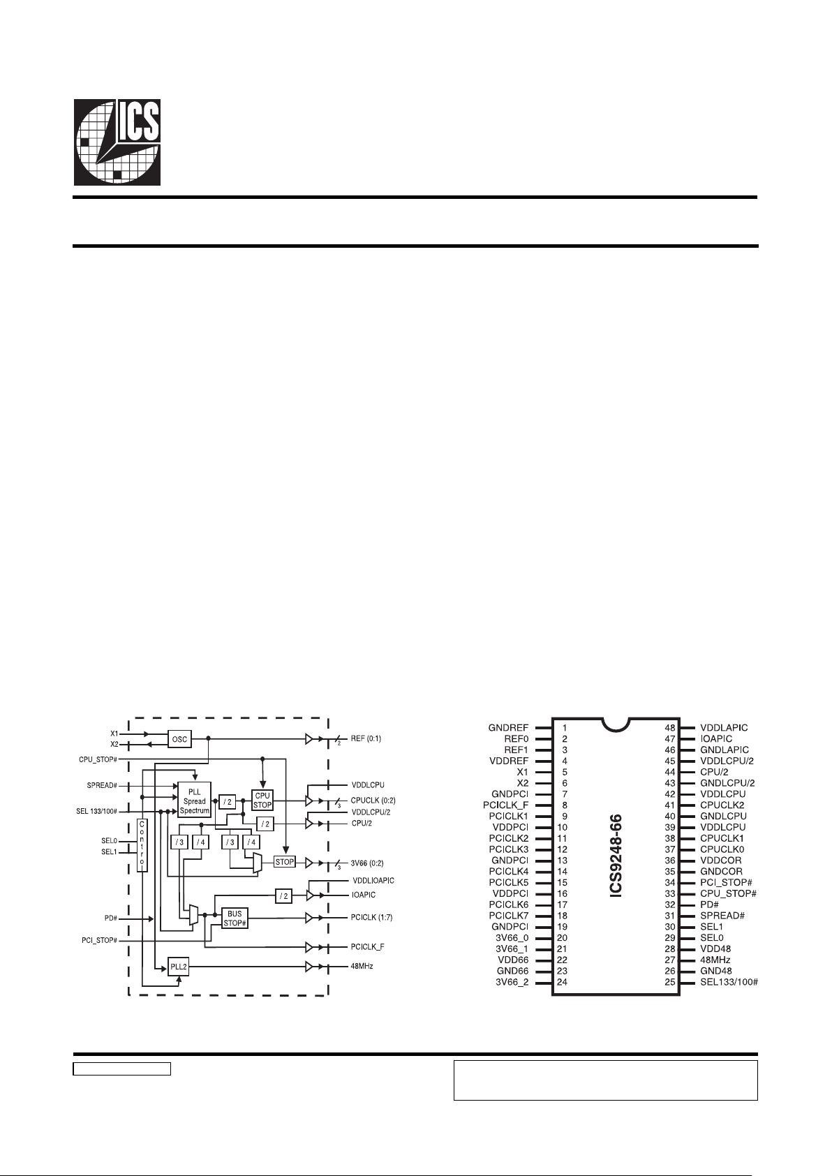
Pin Configuration
48-pin SSOP
Features
Generates the following system clocks:
- 3 CPU clocks ( 2.5V, 100/133MHz)
- 8 PCI clocks, including 1 free-running (3.3V, 33MHz)
- 1 CPU/2 clocks (2.5V, 50/66MHz)
- 1 IOAPIC clocks (2.5V, 16.67MHz)
- 3 Fixed frequency 66MHz clocks(3.3V, 66MHz)
- 2 REF clocks(3.3V, 14.318MHz)
- 1 USB clock (3.3V, 48MHz)
Efficient power management through PD#, CPU_STOP#
and PCI_STOP#.
0 to -0.5% typical down spread modulation on CPU,
PCI, IOAPIC, 3V66 and CPU/2 output clocks.
Uses external 14.318MHz crystal.
Advance Information
ADVANCE INFORMATION documents contain information on products
in the formative or design phase development. Characteristic data and
other specifications are design goals. ICS reserves the right to change or
discontinue these products without notice.
Block Diagram
Key Specification
CPU Output Jitter: <250ps
CPU/2 Output Jitter. <250ps
IOAPIC Output Jitter: <500ps
48MHz, 3V66, PCI Output Jitter: <500ps
Ref Output Jitter. <1000ps
CPU Output Skew: <175ps
PCI Output Skew: <500ps
3V66 Output Skew <250ps
CPU to 3V66 Output Offset: 0.0 - 1.5ns (CPU leads)
3V66 to PCI Output Offset: 1.5 - 4.0ns (3V66 leads)
CPU to IOAPIC Output Offset 1.5 - 4.0ns (CPU leads)
Page 2
2
ICS9248-66
Advance Information
Pin Descriptions
Power Groups:
VDDREF, GNDREF = REF, X1, X2
GNDPCI, VDDPCI = PCICLK
VDD66, GND66 = 3V66
VDD48, GND48 = 48MHz
VDDCOR, GNDCOR = PLL Core
VDDLCPU/2 , GNDLCPU/2 = CPU/2
VDDLIOAPIC, GNDIOAPIC = IOAPIC
The ICS9248-66 is a main clock synthesizer chip for Pentium
II based systems using Rambus Interface DRAMs. This chip
provides all the clocks required for such a system when used
with a Direct Rambus Clock Generator(DRCG) chip such as
the ICS9211-01.
Spread Spectrum may be enabled by driving the SPREAD#
pin active. Spread spectrum typically reduces system EMI
by 8dB to 10dB. This simplifies EMI qualification without
resorting to board design iterations or costly shielding. The
ICS9248-66 employs a proprietary closed loop design, which
tightly controls the percentage of spreading over process
and temperature variations.
The CPU/2 clocks are inputs to the DRCG.
General Description
Pin number Pin name Type Description
1, 7, 13, 19, 23, 26,
35
GND PWR Ground pins
2, 3 REF(0:1) OUT 14.318MHz reference clock outputs at 3.3V
4, 10, 16, 22, 28, 36 VDD PWR Power pins 3.3V
5 X1 IN XTAL_IN 14.318MHz crystal input
6 X2 OUT XTAL_OUT Crystal output
8 PCICLK_F OUT
Free running PCI clock at 3.3V. Synchronous to CPU clocks. Not affected by the
PCI_STOP# in
p
ut.
9, 11, 12, 14,
15, 17, 18
PCICLK[1:7] OU T PCI clock outputs at 3.3V. Synchronous to CPU clocks.
20, 21, 24 3V66[0:2] OUT 66MHz outputs at 3.3V. These outputs are stopped when CPU_STO P# is driven active..
25 SEL 133/100# IN
This selects the frequency for the CPU and CPU/2 outputs. High = 133MHz,
Low=100MHz
27 48MHz OUT Fixed 48MHz clock output. 3.3V
29, 30 SEL[0:1] IN Function select pins. See truth table for details.
31 S PREAD# IN
Enables spread spectrum when active(Low ). modulates all the CPU, PCI , IOAPIC, 3V66
and CPU/2 clocks. Does not affect the REF and 48MHz clocks. 0.5% down spread
modulation.
32 PD# IN
This asynchronous input powers down the chip when drive active(Low). The internal PLLs
are disabled and all the o ut
p
ut clock s are held at a Low state.
33 CPU_STOP# IN
This asychronous input halts the CPUCLK[0:3] and the 3V66[0:3] clocks at logic "0"
wh en driven active( Low). Does not aff ect the CPU/2 clocks.
34 PCI_STOP# IN
This asynchronous input halts the PCICLK[1:7] at logic"0" when driven active(Low).
PC ICLK_F is n ot affected b
y
this input.
40 GN DLCPU PWR Ground pin for the CPUCLKs
37, 38, 41 CPUCLK[0:3] OUT
Host bus clock output at 2.5V . 133MHz or 100MHz depending on the state of the S EL
133/100MHz.
39, 42 VDDLCPU PWR Power pin for the CP UCLKs. 2.5V
43 GNDLCPU/2 PWR Ground pin for the CPU/2 clocks.
44 CPU/2 OUT
2.5V clock outputs at 1/2 CPU frequency. 66MHz or50MHz depending on the state of the
SEL 133/100# in
p
ut pin.
45 VDDLCPU/2 PWR Power pin for the CPU/2 clocks. 2.5V
46 G NDLIOAPIC PWR Ground pin for the IOAPIC outputs.
47 IOAPIC OUT IOAPIC clocks at 2.5V. Synchronous with CPUCLKs but fixed at 16.67MHz.
48 V DDLIOAPIC PWR Power pin for the IOAPIC outputs. 2.5V.
Page 3
3
ICS9248-66
Advance Information
Frequency Select:
Note:
1. TCLK is a test clock driven on the x1 input during test mode.
#POTS_UPC#DP#POTS_ICPKLCUPC2/UPCCIPAOI66V3ICPF_ICP
.FER
zHM84
csOsOCV
X0XWOLWOLWOLWOLWOLWOLWOLFFOFFO
010WOLNONOWOLWOLNONONONO
011WOLNONOWOLNONONONONO
110NONONONOWOLNONONONO
111NONONONONONONONONO
LES
-001/331
#
1LES0LES
UPC
zHM
2/UPC
zHM
66V3
zHM
ICP
zHM
84
zHM
FER
zHM
CIPAOI
zHM
stnemmoC
000 Z-iHZ-iHZ-iHZ-iHZ-iHZ-iHZ-iHetats-irT
001A/NA/NA/NA/NA/NA/NA/NdevreseR
010 001056.663.33Z-iH813.4176.61
LLPzHM84
delbasid
011 001056.663.3384813.4176.61
100 2/KLCT4/KLCT4/KLCT8/KLCT
-/KLCT
2
KLCT61/KLCT)1(edomtseT
101 A/NA/NA/NA/NA/NA/NA/NdevreseR
110 3.3316.666.663.33Z-iH813.4176.61
111 3.3316.666.663.3384813.4176.61
ICS9248-66 Power Management Features:
Note:
1. LOW means outputs held static LOW as per latency requirement next page.
2. On means active.
3. PD# pulled Low, impacts all outputs including REF and 48 MHz outputs.
4. All 3V66 as well as all CPLU clocks should stop cleanly when CPU_STOP# is pulled LOW.
5. CPU/2, IOAPIC, REF, 48 MHz signals are not controlled by the CPU_STOP# functionality and are enabled all in all conditions
except PD# = LOW
Page 4
4
ICS9248-66
Advance Information
Power Management Requirements:
Note:
1. Clock on/off latency is defined in the number of rising edges of free running PCICLKs between the clock disable goes low/
high to the first valid clock comes out of the device.
2. Power up latency is when PWR_DWN# goes inactive (high to when the first valid clocks are dirven from the device.
lagniSetatSlagniS
ycnetaL
fosegdegnisirfo.oN
KLCICP
POTS_UPC
)delbasid(01
)delbane(11
#POTS_ICP
)delbasid(01
)delbane(11
#DP
)noitarepolamron(1Sm3
)nwodrewop(0.xam2
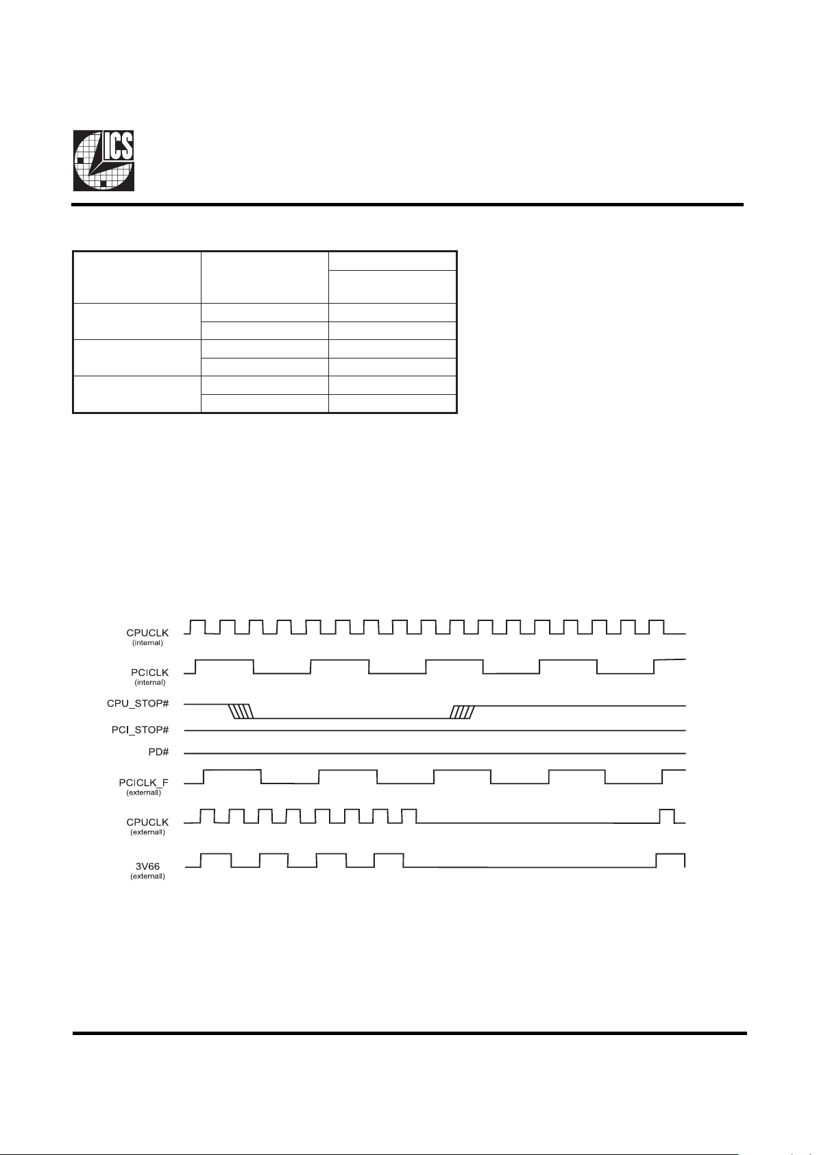
CPU_STOP# Timing Diagram
CPU_STOP# is an asynchronous input to the clock synthesizer. It is used to turn off the CPU and 3V66 clocks for low power
operation. CPU_STOP# is asserted asynchronously by the external clock control logic with the rising edge of free running PCI
clock (and hence CPU clock) and must be internally synchronized to the external output. All other clocks will continue to run
while the CPU clocks are disabled. The CPU clocks must always be stopped in a low state and started in such a manner as to
guarantee that the high pulse width is a full pulse. ONLY one rising edge of PCICLK_F is allowed after the clock control logic
switched for both the CPU and 3V66 outputs to become enabled/disabled.
Notes:
1. All timing is referenced to the internal CPUCLK.
2. The internal label means inside the chip and is a reference only. This in fact may not be the way that the control is designed.
3. CPU_STOP# signal is an input singal that must be made synchronous to free running PCICLK_F
4. 3V66 clocks also stop/start before
5. PD# and PCI_STOP# are shown in a high state.
6. Diagrams shown with respect to 133MHz. Similar operation when CPU is 100MHz
Page 5

5
ICS9248-66
Advance Information
PCI_STOP# Timing Diagram
PCI_STOP# is an input to the clock synthesizer and must be made synchronous to the clock driver PCICLK_F output. It is used
to turn off the PCI clocks for low power operation. PCI clocks are required to be stopped in a low state and started such that a
full high pulse width is guaranteed. ONLY one rising edge of PCICLK_F is allowed after the clock control logic switched for the
PCI outputs to become enabled/disabled.
Notes:
1. All timing is referenced to CPUCLK.
2. PCI_STOP# signal is an input signal which must be made synchronous to PCICLK_F output.
3. Internal means inside the chip.
4. All other clocks continue to run undisturbed.
5. PD# and CPU_STOP# are shown in a high state.
6. Diagrams shown with respect to 133MHz. Similar operation when CPU is 100MHz.
Page 6

6
ICS9248-66
Advance Information
PD# Timing Diagram
The power down selection is used to put the part into a very low power state without turning off the power to the part. PD# is
an asynchronous active low input. This signal needs to be synchronized internal to the device prior to powering down the clock
synthesizer.
PD# is an asynchronous function for powering up the system. Internal clocks are not running after the device is put in power
down. When PD# is active low all clocks need to be driven to a low value and held prior to turning off the VCOs and crystal. The
power up latency needs to be less than 3 mS. The power down latency should be as short as possible but conforming to the
sequence requirements shown below. PCI_STOP# and CPU_STOP# are considered to be don't cares during the power down
operations. The REF and 48MHz clocks are expected to be stopped in the LOW state as soon as possible. Due to the state of
the internal logic, stopping and holding the REF clock outputs in the LOW state may require more than one clock cycle to
complete.
Notes:
1. All timing is referenced to the Internal CPUCLK (defined as inside the ICS9148 device).
2. Internal means inside the chip
3. PD# is an asynchronous input and metastable conditions may exist. This signal is synchronized inside this part.
4. The shaded sections on the VCO and the Crystal signals indicate an active clock.
5. Diagrams shown with respect to 133MHz. Similar operation when CPU is 100MHz.
Page 7

7
ICS9248-66
Advance Information
Absolute Maximum Ratings
Supply Voltage . . . . . . . . . . . . . . . . . . . . . . . . . . . 7.0 V
Logic Inputs . . . . . . . . . . . . . . . . . . . . . . . . . . . . GND 0.5 V to VDD +0.5 V
Ambient Operating Temperature . . . . . . . . . . . . 0°C to +70°C
Storage Temperature . . . . . . . . . . . . . . . . . . . . . . 65°C to +150°C
Stresses above those listed under Absolute Maximum Ratings may cause permanent damage to the device. These ratings are
stress specifications only and functional operation of the device at these or any other conditions above those listed in the
operational sections of the specifications is not implied. Exposure to absolute maximum rating conditions for extended periods
may affect product reliability.
Electr i cal Character i st i cs - I nput/Supply/ Comm on O utput Paramet er s
TA = 0 - 70C; Supply Vol tage VDD = 3.3 V +5%, VDDL=2.5 V+ 5%(unless o t he rw ise stated)
PARAMETER SYMBOL COND ITI O NS MIN TYP MAX UNI TS
Input High Voltage V
IH
2
V
DD
+0.
3
V
Input Low Voltage V
IL
VSS-0.3 0.8 V
Inpu t High Current I
IH
VIN = V
DD
-5 5
µ
A
Input L ow Cur rent I
IL1
VIN = 0 V; Input s with no pull-up resistors
µ
A
Input L ow Cur rent I
IL2
VIN = 0 V; Input s with pull-up resistors
µ
A
Operating Supply
Current
I
DD3.3OP
CL = 0 pF; Sel e ct mA
Power Down Supply
Current
I
DD3.3PD
CL = 0 pF; Wit h inpu t a d dress to Vd d or GND
µ
A
Input frequency F
i
VDD = 3 .3 V; 14.318 MH z
Pin Inductance L
pin
7nH
C
IN
Logic Inputs 5 pF
C
out
O ut put pi n c apacitanc e 6 pF
C
INX
X 1 & X2 pin s 27 45 pF
Tr ansition Time
1
T
trans
To 1st crossing of target Freq. 3 m S
Settling Time
1
T
s
From 1st crossing to 1% t a rget Freq. mS
Clk Stabiliza tion
1
T
STAB
From VDD = 3.3 V t o 1% targ e t Fre q. 3 m S
t
PZH,tPZH
output ena b l e d e l ay (all out p uts) 1 10 nS
t
PLZ,tPZH
output disable delay (al l ou t put s) 1 10 nS
1
G ua rentee d by d e sign, not 100% tested in produc t i on .
Input Capacita nce
1
Delay
Group Offset
Group Offset Measurement Loads Measure Points
CPU to 3V66 0.0-1.5ns CPU leads CPU @ 20pF, 3V66 @ 30pF CPU @1.25V, 3V66 @ 1.5V
3V66 to PCI 1.5-4.0ns 3V66 leads 3V66 @ 30pF, PCI @ 30pF 3V66 @ 1.5V, PCI @ 1.5V
CPU to IOAPIC 1.5-4.0ns CPU leads CPU @ 20pF, IOAPIC @ 20pF CPU @1.25V, IOAPIC @ 1.5V
N ot e: 1. All of fsets are t o be measured at risi ng edges.
Page 8

8
ICS9248-66
Advance Information
Electri cal Character i sti cs - CPU
TA = 0 - 70C, V
DDL
= 2.5 V +/- 5%; CL = 1 0 - 20 pF (unles s other wise stated)
PARAMETER SYMBOL COND ITI ON S MIN TYP MAX UNITS
O utp ut Imped a nc e R
DSP2B
1
VO = VDD*(0.5) 13.5 45
Ω
Output High Voltage V
OH2B
IOH = -1 mA 2 V
Output Low Voltage V
OL2B
IOL = 1 mA 0.4 V
O utput High Cur rent I
OH2B
V
OH @MIN
= 1.0V , V
OH@ MAX
= 2 .375V -27 -27 mA
Ou tput Low Cu rre nt I
OL2B
V
OL @MIN
= 1.2V , V
OL@ MAX
= 0.3V 27 30 mA
Rise Time t
r2B
1
VOL = 0.4 V, VOH = 2 .0 V 0.4 1.6 ns
Fall Time t
f2B
1
VOH = 0.4 V, VOL = 2 .0 V 0.4 1.6 ns
Duty Cycle d
t2B
1
VT = 1.25 V 45 55 ns
Skew t
sk2B
1
VT = 1.25 V 175 ps
Jitter
t
jcyc-cyc
1
VT = 1.25 V
250 ps
1
G ua rentee d by de sign, not 100% teste d i n production.
Electri cal Characteri sti cs - CPU/2
TA = 0 - 70C, V
DDL
= 2.5 V +/-5%; CL = 1 0 - 20 pF (unles s otherwise stated)
PARAMETER SYMBOL CON DITI O NS MIN TYP MAX UNITS
O utp ut Imped a nc e R
DSP2B
1
VO = VDD*(0.5) 13.5 45
Ω
Output High Voltage V
OH2B
IOH = -1 mA 2 V
Output Low Voltage V
OL2B
IOL = 1 mA 0.4 V
O utput High Cur rent I
OH2B
V
OH @MIN
= 1.0V , V
OH@ MAX
= 2 .375V -27 -27 m A
Ou tput L ow Cur rent I
OL2B
V
OL @MIN
= 1.2V , V
OL@ MAX
= 0.3V 27 30 mA
Rise Time t
r2B
1
VOL = 0.4 V, VOH = 2 .0 V 0.4 1.6 ns
Fa ll T ime t
f2B
1
VOH = 0.4 V, VOL = 2 .0 V 0.4 1.6 ns
Duty Cycle d
t2B
1
VT = 1.25 V 45 55 ns
Jitter
t
jcyc-cyc
1
VT = 1.25 V
250 ps
1
G ua renteed by de sign, not 100% teste d in production.
Page 9

9
ICS9248-66
Advance Information
Electrical Characteristi cs - PCI
TA = 0 - 70C; VDD = 3.3 V +/-5%; CL = 1 0-30 pF (unless oth erwise state d)
PARA METER SY MBOL CO ND ITIO NS MIN TYP MAX UN ITS
O utp ut I mpedanc e R
DSP1
1
VO = VDD*(0.5) 12 55
Ω
O utp ut I mpedanc e R
DSN1
1
VO = VDD*(0.5) 12 55
Ω
Output High Voltage V
OH1
IOH = -1 mA 2.4 V
Output Low Voltage V
OL1
IOL = 1 mA 0.55 V
O utput High Cur r e nt I
OH1
VOH@ MIN = 1.0 V, VOH@ MAX = 3.135 V - 29 -23 m A
O utput Low Cu r rent I
OL1
VOL@ MIN = 1.95 V, VOL@ MAX= 0.4 29 27 mA
Rise Time t
r1
1
VOL = 0.4 V, VOH = 2. 4 V 0.5 2 ns
F all Time t
f1
1
VOH = 2. 4 V, VOL = 0. 4 V 0.5 2 ns
Duty Cycle d
t1
1
VT = 1.5 V 45 55 %
Skew t
sk1
1
VT = 1 . 5 V 500 ps
Jitte r
t
jcyc-cycVT
= 1.5 V
500 ps
1
G ua r e nte e d by d es ign, not 100% te s te d in production.
Electrical Characteristi cs - 3V66
TA = 0 - 70C; VDD = 3. 3 V + /- 5% ; CL = 10-30 pF ( u nle s s o the rwise state d)
PARA METER SYMBOL CONDITIONS MIN TYP MAX UNITS
O utp ut Impe da nc e R
DSP1
1
VO = VDD*(0.5) 12 5 5
Ω
O utp ut Impe da nc e R
DSN1
1
VO = VDD*(0.5) 12 5 5
Ω
Output High Voltage V
OH1
IOH = -1 mA 2.4 V
Output Low Voltage V
OL1
IOL = 1 mA 0.55 V
Output High Current I
OH1
VOH@ MIN = 1.0 V, VOH@ MAX = 3.135 V -33 -33 mA
Output Low Current I
OL1
VOL@ MIN = 1.95 V, VOL@ MAX= 0.4 30 38 mA
Rise Time t
r1
1
VOL = 0.4 V, VOH = 2. 4 V 0.5 2.0 ns
Fa ll Time t
f1
1
VOH = 2. 4 V , VOL = 0. 4 V 0.5 2.0 ns
Duty Cycle d
t1
1
VT = 1.5 V 45 55 %
Skew t
sk1
1
VT = 1.5 V 250 ps
Jitte r
t
jcyc-cyc
VT = 1.5 V
500 ps
1
G uar enteed by design, not 100% tested in production.
Page 10

10
ICS9248-66
Advance Information
Electrical Characteristics - IO A PIC
TA = 0 - 70C, V
DDL
= 2.5 V +/-5%; CL = 10 - 20 pF ( u nles s othe r wise sta ted)
PARA METER SYMBOL CON DITIO NS MIN TYP MAX UN ITS
O utput Impe danc e
R
DSP2B
1
VO = VDD*(0.5) 13.5 45
Ω
O utput High V o ltage V
OH2B
IOH = -1 mA 2 V
Output Low Voltage V
OL2B
IOL = 1 mA 0.4 V
O utput High Cur rent I
OH2B
V
OH @MIN
= 1.0V , V
OH@ MAX
= 2.375V -27 -27 mA
O utput L ow Curr e nt I
OL2B
V
OL @MI N
= 1.2V , V
OL@ MAX
= 0. 3V 27 30 mA
Rise Time
t
r2B
1
VOL = 0. 4 V, VOH = 2. 0 V 0.4 1.6 ns
Fa ll T im e
t
f2B
1
VOH = 0.4 V, VOL = 2. 0 V 0.4 1.6 ns
Duty Cycle
d
t2B
1
VT = 1. 25 V 45 55 ns
Skew
t
sk2B
1
VT = 1. 25 V NA ps
Jitter
t
jcy
c-cyc
1
VT = 1. 25 V 500 ps
1
G ua r e ntee d by de s ign, not 100% tested in production.
Electrical Characteristics - 48M , REF
TA = 0 - 70C; VDD = V
DDL
= 3.3 V +/-5%; CL = 10 - 20 pF (unle s s otherwis e s tated)
PARA METER SYMBO L CONDITIO N S MIN TYP MAX UNITS
O utput I mpedanc e
R
DSP5
1
VO = VDD*(0.5) 20 60
Ω
O utput I mpedanc e
R
DSN5
1
VO = VDD*(0.5) 20 60
Ω
Output High Voltage V
OH5
IOH = 1 mA 2.4 V
Output Low Voltage V
OL5
IOL = -1 mA 0.4 V
O utput H igh C ur r ent I
OH5
V
OH @MIN
=1 V, V
OH@MAX
= 3.135 V -29 -23 m A
O utput L ow Cur rent I
OL5
V
OL@MIN
=1.95 V, V
OL@MIN
=0.4 V 29 27 mA
Duty Cycle
d
t5
1
VT = 1. 5 V 45 55 %
t
jcy
c-cyc
1
VT = 1. 5 V; Fixe d C locks 500 ps
t
jcy
c-cyc
1
VT = 1. 5 V; Ref Cloc ks 1000 ps
Skew T
sk
VT = 1. 5 V,F ixed C locks N /A ps
1
G uarenteed by de s ign, not 100% tested in pr odu ction.
Jitte r
Page 11

11
ICS9248-66
Advance Information
LOBMYS SNOISNEMIDNOMMOC SNOITAIRAV D N
.NIM.MON.XAM.NIM.MON.XAM
A590.101.011.DA027.527.037.65
1A800.210.610.
2A880.090.290.
B800.010.5310.
C500.- 010.
DsnoitairaVeeS
E292.692.992.
eCSB520.0
H004.604.014.
h010.310.610.
L420.230.040.
NsnoitairaVeeS
∝
°0°5°8
X580.390.001.
56 Pin SSOP Package
ADVANCE INFORMATION documents contain information on products
in the formative or design phase development. Characteristic data and
other specifications are design goals. ICS reserves the right to change or
discontinue these products without notice.
Ordering Information
ICS9248yF-66
Pattern Number (2 or 3 digit number for parts with ROM code patterns)
Package Type
F=SSOP
Revision Designator (will not correlate with datasheet revision)
Device Type (consists of 3 or 4 digit numbers)
Prefix
ICS, AV = Standard Device
Example:
ICS XXXX y F - PPP
 Loading...