

Page 1
Integrated
Circuit
Systems, Inc.
ICS9248-65
Third party brands and names are the property of their respective owners.
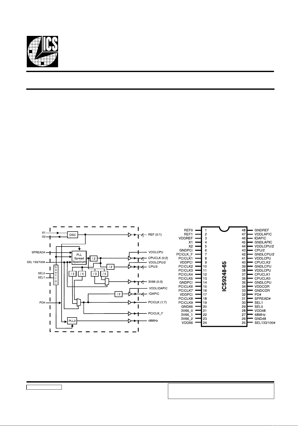
Block Diagram
Frequency Timing Generator for PENTIUM IISystems
9248-65 Rev C 7/28/99
Pin Configuration
48-pin SSOP
Generates the following system clocks:
- 3 CPU clocks ( 2.5V, 100/133MHz)
- 10 PCI clocks, including 1 free-running
(3.3V, 33.3MHz)
- 1 CPU/2 clocks (2.5V, 50/66.6MHz)
- 1 IOAPIC clocks (2.5V, 16.67MHz)
- 3 Fixed frequency 66MHz clocks(3.3V, 66.6MHz)
- 2 REF clocks(3.3V, 14.318MHz)
- 1 USB clock (3.3V, 48MHz)
Efficient power management through PD#.
0 to -0.5% typical down spread modulation on CPU, PCI,
IOAPIC, 3V66 and CPU/2 output clocks.
Uses external 14.318MHz crystal.
ICS reserves the right to make changes in the device data identified in
this publication without further notice. ICS advises its customers to
obtain the latest version of all device data to verify that any
information being relied upon by the customer is current and accurate.
Features
Key Specification
CPU Output Jitter: <250ps
CPU/2 Output Jitter. <250ps
IOAPIC Output Jitter: <500ps
48MHz, 3V66, PCI Output Jitter: <500ps
PCI Output Jitter. <500ps
Ref Output Jitter. <1000ps
CPU 0:2 Output Skew: <175ps
PCI_F, PCI 1:7 Output Skew: <500ps
3V66_0:2 Output Skew <250ps
CPU to 3V66_0:2 Output Offset: 0.0 - 1.5ns (CPU leads)
3V66 to PCI Output Offset: 1.5 - 4ns (CPU leads)
CPU to IOAPIC Output Offset 1.5 - 4.0ns (CPU leads)
Page 2
2
ICS9248-65
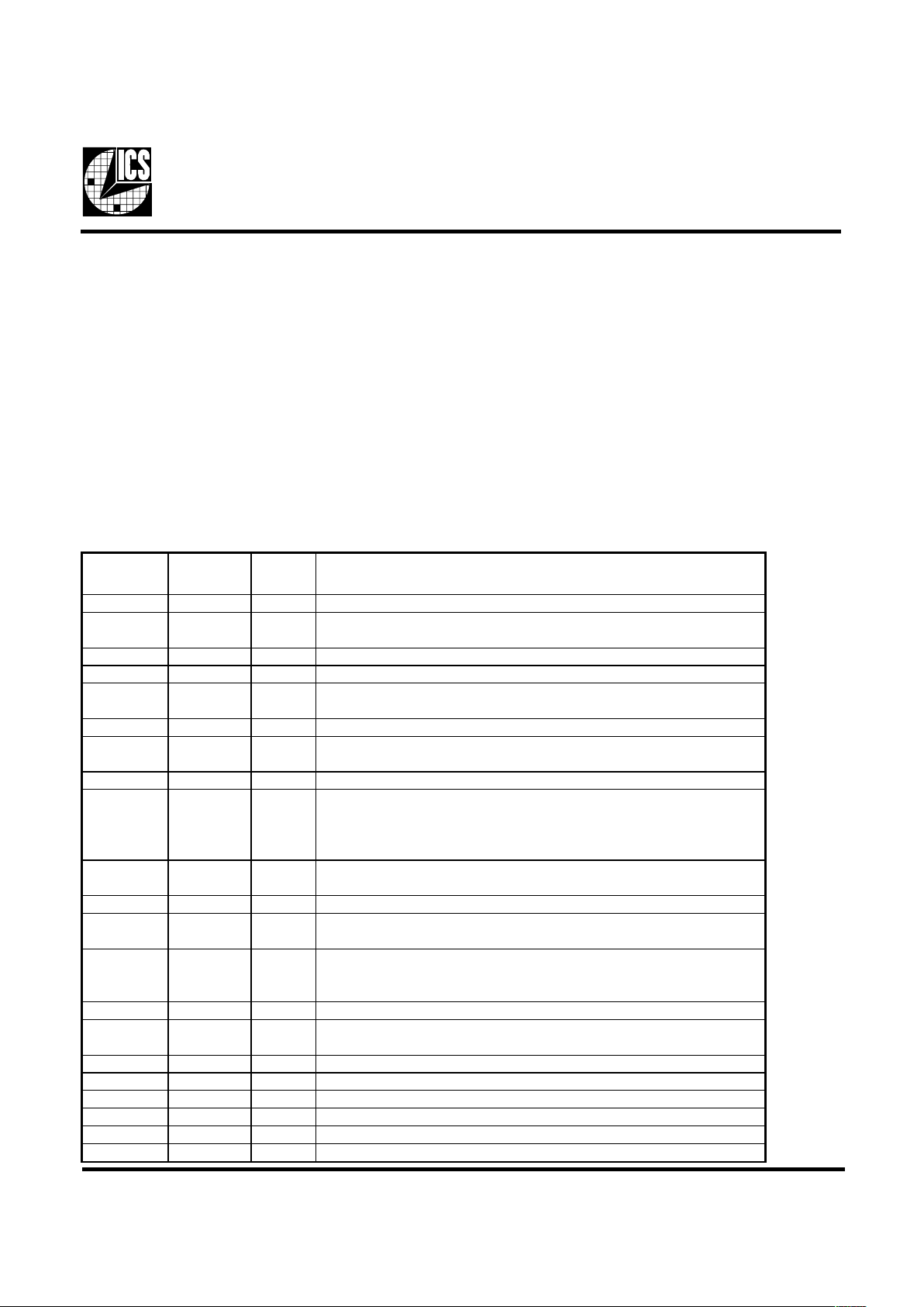
Pin Descriptions
Pin number Pin name Type Description
1,2 REF Output 3.3V, 14.318 MHz re f e r e nce clock output.
3, 9, 17, 24,
28, 34
VDD Power 3.3 V power for clock outputs .
4 X1 Input 14.318 MHz cr ystal input
5 X2 Output 14.318 MHz cr ystal output
6,14, 20, 26,
33, 45, 48
GND Power Ground for cloc k outputs
7 PCICLK_F Output 3.3 V free running PCI clock output, will not be stopped by t he PCI_STOP#
8,10,11,12,13,
15,16,18,19
PCICLK (1:9) Output 3.3 V P C I cloc k outputs , generating timing r e quir ements f or
21,22, 23 3V66 Output 3.3 V 66 MHz c loc k output, fixed frequency cloc k typic al ly used with AGP
25
SEL
133/100#
Input
Control for the frequency of clocks a t the C PU output pins . If l ogic "0" is used the
100 MH z frequenc y is selecte d. If Logic "1" is used, the 133 MHz f requency is
sele c ted. The P C I clock is multiplexed to run a t 33. 3 M Hz f or both selecte d c a s e s .
27 48 MHz Output
3.3 V 48 MHz c loc k output, fixed frequency cloc k typic al ly used with USB
devices
29,30 SEL (0:1) Input Frequency se le ct pi n , logic input.
31 SPREAD# Output
Power-on spr ea d spectrum enable option. Active low = s pread spect rum clocking
enable. Active high = spre a d spectrum clocking disable .
32 PD# Input
Asynchronous ac t ive low input pin used to power down the device into a low
power s tate. The internal clocks are disabled and the V CO and the crystal ar e
stopped.
35,39 GNDLCPU Power Ground for the CPU and H ost clock outputs
36,37,40
CPUCLK
(0:2)
0utput 2.5 V CPU and H ost clock outputs
38,41 VDDLCPU Power 2.5 V powe r for the C PU and Host cloc k outputs
42 GNDLCPU/2 Powe r Ground for the CPU and Host cloc k outputs
43 CPU/2 Output Out put running at 1/2 CPU clock f requency. Synchronous to the C PU outputs .
44 VDDL C P U/2 Pow er 2.5 V pow e r f or the CPU/2 clock outputs
46 IOAPI C (0:1) Output 2.5V fixed 16. 6 M Hz IOA PIC cl ock outputs
47 VDDIOAPIC Power 2.5V power for IOAPIC clock
The ICS9248-65 is a main clock synthesizer chip for Pentium
II based systems using Rambus Interface DRAMs. This chip
provides all the clocks required for such a system when used
with a Direct Rambus Clock Generator(DRCG) chip such as
the ICS9211-01.
Spread Spectrum may be enabled by driving the SPREAD#
pin active. Spread spectrum typically reduces system EMI by
8dB to 10dB. This simplifies EMI qualification without
resorting to board design iterations or costly shielding. The
ICS9248-65 employs a proprietary closed loop design, which
tightly controls the percentage of spreading over process
and temperature variations.
The CPU/2 clocks are inputs to the DRCG.
General Description Power Groups:
VDDREF, GNDREF = REF, X1, X2
GNDPCI, VDDPCI = PCICLK
VDD66, GND66 = 3V66
VDD48, GND48 = 48MHz
VDDCOR, GNDCOR = PLL Core
VDDLCPU/2 , GNDLCPU/2 = CPU/2
VDDLIOAPIC, GNDIOAPIC = IOAPIC
Page 3
3
ICS9248-65
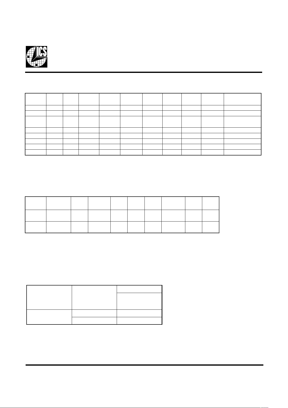
Frequency Select:
Note:
1. TCLK is a test clock driven on the x1 input during test mode.
ICS9248-65 Power Management Features:
Note:
1. LOW means outputs held static LOW as per latency requirement next page.
2. On means active.
3. PD# pulled Low, impacts all outputs including REF and 48 MHz outputs.
LES
#001/331
1LES0LES
UPC
zHM
2/UPC
zHM
66V3
zHM
ICP
zHM
84
zHM
FER
zHM
CIPAOI
zHM
stnemmoC
000 Z-iHZ-iHZ-iHZ-iHZ-iHZ-iHZ-iHetats-irT
001A/NA/NA/NA/NA/NA/NA/NdevreseR
010 001056.663.33Z-iH813.4176.61
LLPzHM84
delbasid
011 001056.663.3384813.4176.61
100 2/KLCT4/KLCT4/KLCT8/KLCT2/KLCTKLCT61/KLCT)1(edomtseT
101 A/NA/NA/NA/NA/NA/NA/NdevreseR
110 3.331666633Z-iH813.4176.61
111 3.33166663384813.4176.61
#DPKLCUPC2/UPCCIPAOI66V3ICPF_ICP
.FER
zHM84
csOsOCV
0WOLWOLWOLWOLWOLWOLWOLFFOFFO
1NONONONONONONONONO
Power Management Requirements:
Note:
1. Clock on/off latency is defined in the number of rising edges of free running PCICLKs between the clock disable goes low/
high to the first valid clock comes out of the device.
2. Power up latency is when PWR_DWN# goes inactive (high to when the first valid clocks are dirven from the device.
lagniSetatSlagniS
ycnetaL
segdegnisirfo.oN
KLCICPfo
#DP
)noitarepolamron(1Sm3
)nwodrewop(0.xam2
Page 4

4
ICS9248-65
PD# Timing Diagram
The power down selection is used to put the part into a very low power state without turning off the power to the part. PD# is
an asynchronous active low input. This signal needs to be synchronized internal to the device prior to powering down the clock
synthesizer.
Internal clocks are not running after the device is put in power down. When PD# is active low all clocks need to be driven to a
low value and held prior to turning off the VCOs and crystal. The power up latency needs to be less than 3 mS. The power down
latency should be as short as possible but conforming to the sequence requirements shown below. PCI_STOP# and CPU_STOP#
are considered to be don't cares during the power down operations. The REF and 48MHz clocks are expected to be stopped in
the LOW state as soon as possible. Due to the state of the internal logic, stopping and holding the REF clock outputs in the
LOW state may require more than one clock cycle to complete.
Notes:
1. All timing is referenced to the Internal CPUCLK (defined as inside the ICS9248 device).
2. As shown, the outputs Stop Low on the next falling edge after PD# goes low.
3. PD# is an asynchronous input and metastable conditions may exist. This signal is synchronized inside this part.
4. The shaded sections on the VCO and the Crystal signals indicate an active clock.
5. Diagrams shown with respect to 133MHz. Similar operation when CPU is 100MHz.
Page 5

5
ICS9248-65
Absolute Maximum Ratings
Supply Voltage . . . . . . . . . . . . . . . . . . . . . . . . . . . 7.0 V
Logic Inputs . . . . . . . . . . . . . . . . . . . . . . . . . . . . GND 0.5 V to VDD +0.5 V
Ambient Operating Temperature . . . . . . . . . . . . 0°C to +70°C
Storage Temperature . . . . . . . . . . . . . . . . . . . . . . 65°C to +150°C
Stresses above those listed under Absolute Maximum Ratings may cause permanent damage to the device. These ratings are
stress specifications only and functional operation of the device at these or any other conditions above those listed in the
operational sections of the specifications is not implied. Exposure to absolute maximum rating conditions for extended periods
may affect product reliability.
Electrical C haracterist ics - I nput/Supply/Comm on O utput Parameters
TA = 0 - 70º C; Supply Voltage VDD = VDDL = 3.3 V +/-5%, (unless otherwise stated)
PARAMETER SYMBOL CONDITIONS MIN TYP MAX UNITS
Input High Voltage V
IH
2V
DD
+0.3 V
Input L ow Vol ta ge V
IL
VSS-0.3 0.8 V
Inpu t High Curre nt I
IH
VIN = V
DD
0.1 5
µ
A
Input Low Current I
IL1
VIN = 0 V; I nput s wi th n o pu l l-up r esist o rs -5 2.0
µ
A
Input Low Current I
IL2
VIN = 0 V; Input s with pul l-up re sistors -200 -100
µ
A
I
DD3.3OP100CL
= 0 pF; Select @ 100 MHz
65
I
DD3.3OP133CL
= 0 pF; Select @ 133.3 MHz
71
I
DD3.3OP144CL
= 0 pF; Select @ 144 MHz
75
I
DD3.3OP154CL
= 0 pF; Select @ 154 MHz
78
Power Down
I
DD3.3P DCL
= 0 pF ; PWRDWN # = 0
64 200
µ
A
Suppl y C urr e nt
Input fre que nc y F
i
VDD = 3 .3 V 12 14.318 16 MHz
Inpu t C a pacitanc e
1
C
IN
Logic Inputs 5 pF
C
INX
X 1 & X2 pi ns 27 36 45 pF
Transition Time
1
T
trans
To 1st cros sing of target Fr eq. 1 3 ms
Settling Time
1
T
s
From 1st cr ossing to 1% tar ge t Freq. 0.5 ms
Clk Stabilization
1
T
STAB
From VDD = 3.3 V t o 1% t a rget Fre q. 3 ms
Skew
1
t
CPU-PCIVT
= 1.5 V; VTL = 1.25 V 1.5 2.4 4 ns
Skew
1
t
CPU-3V66VT
= 1.5 V; VTL = 1.25 V 1.4 1.5 ns
Skew
1
t
3V66-PCIVT
= 1.5 V
1.4 4 ns
1
G ua rante e d by de sign, not 100% tested in produ c t i on.
Operating 160 mA
Group Offse t
Group Of fset Measureme nt Loads Measure Points
CPU to 3V66 0.0-1.5ns CPU leads CPU @ 20pF, 3V66 @ 30pF CPU @1.25V, 3V66 @ 1.5V
3V66 to PCI 1.5-4.0ns 3V66 leads 3V66 @ 30pF, PCI @ 30pF 3V66 @ 1.5V, PCI @ 1.5V
CPU to IOAPIC 1.5-4.0ns CPU leads CPU @ 20pF, IOAPIC @ 20pF CPU @1.25V, IOAPIC @ 1.5V
N ot e: 1. All offsets ar e to be measured at rising edges.
Page 6

6
ICS9248-65
Electrical Characteristics - Input/Supply/Common Output Parameter
s
TA = 0 - 70º C; Supply Voltage VDD = 3.3 V +/-5%, V
DDL
= 2.5 V +/-5% (unless otherw ise stated)
PARAMETER SYMBOL CONDITIONS MIN TY P MAX UNITS
I
DD2.5OP100CL
= 0 pF; Select @ 100 MHz 14 30
Operating I
DD2.5OP133CL
= 0 pF; Select @ 133.3 MHz 18 30
Supply Current I
DD2.5OP144CL
= 0 pF; Select @ 144 MHz 19 30
I
DD2.5OP154CL
= 0 pF; Select @ 154 MHz 20 30
Power Down
I
DD2.5PD
CL = 0 pF; PWR DWN # = 0 0.3 1 00
µ
A
Supply Current
Skew
1
t
CPU-PCI
VT = 1.5 V; VTL = 1.25 V 1.5 2.4 4 ns
Skew
1
t
CPU-3V66
VT = 1.5 V; VTL = 1.25 V 1.4 1.5 ns
Skew
1
t
CPU-IOAPICVTL
= 1.25 V
1.4 4 ns
1
Guar antee d by desi gn, not 100% tested i n production.
mA
Ele ctrical C haracteristics - CP UCLK
TA = 0 - 70º C; VDD = 3.3 V +/-5%, V
DDL
= 2.5 V +/-5%; CL = 20 pF (unl ess ot he rw i se stated)
PARAMETER SYMBOL CONDITIONS MIN TYP MAX UNITS
Output High Voltage V
OH2B
IOH = -12.0 mA 2 2. 3 V
Output Low Voltage V
OL2B
IOL = 12 mA 0.31 0.4 V
O utput High Curre nt I
OH2B
VOH = 1 .7 V -39 -19 mA
Ou tput Low C urr e nt I
OL2B
VOL = 0.7 V 19 27 mA
Rise Time
t
r2B
1
VOL = 0.4 V, VOH = 2.0 V 0.95 1.6 ns
Fall Time
t
f2B
1
VOH = 2.0 V, VOL = 0 .4 V 1 1.6 ns
Duty Cycle
d
t2B
1
VT = 1.25 V, Freq. < 124 M Hz 45 50 55 %
Skew
t
sk2B
1
VT = 1.25 V 22 175 ps
Jitter, One Sigma
t
j1σ2B
1
VT = 1.25 V 21 150 ps
Jitter, Absolute
t
jabs2B
1
VT = 1.25 V -2 50 55 +250 ps
Jitter, Cycle-to-cycle
t
jcyc-cyc2B
1
VT = 1.25 V
110 250 ps
1
G ua rante e d by de sign, not 100% tested in produ c t i on.
Page 7

7
ICS9248-65
Ele ctrical C h aracteristics - C PU/ 2
TA = 0 - 70º C; VDD = 3.3 V +/-5%, V
DDL
= 2.5 V +/-5%; CL = 20 pF (unl ess ot he rw i se stated)
PARAMETER SYMBOL CONDITIONS MIN TYP MAX UNITS
Output High Voltage V
OH2B
IOH = -12.0 mA 2 2. 3 V
Output Low Voltage V
OL2B
IOL = 12 mA 0.31 0.4 V
O utput High Curre nt I
OH2B
VOH = 1 .7 V -33 -19 mA
Ou tput Low C urr e nt I
OL2B
VOL = 0.7 V 19 27 mA
Rise Time t
r2B
1
VOL = 0.4 V, VOH = 2 .0 V 1.1 1.6 ns
Fall Time t
f2B
1
VOH = 2.0 V, VOL = 0 .4 V 1 1.6 ns
Duty Cycle d
t2B
1
VT = 1.25 V, Freq. < 124 M Hz 45 48 55 %
Jitter, One Sigma t
j1σ2B
1
VT = 1.25 V 13 150 ps
Jitter, Absolute t
jabs2B
1
VT = 1.25 V -2 50 42 +250 ps
Jitter, Cycle-to-cycle
t
jcyc-cyc2B
1
VT = 1.25 V
100 250 ps
1
G ua rante e d by de sign, not 100% tested in produ c t i on.
Ele ctrical C h aracteristics - 3V 66
TA = 0 - 70º C; VDD = 3.3 V +/-5%, V
DDL
= 2.5 V +/-5%; CL = 30 pF (unl ess ot he rw i se stated)
PARAMETER SYMBOL CONDITIONS MIN TYP MAX UNITS
O utput High Vol ta g e V
OH1
IOH = -11 mA 2.4 3.1 V
Output Low Voltage V
OL1
IOL = 9.4 mA 0.17 0.4 V
Ou tput High C urr e nt I
OH1
VOH = 2.0 V -61 -22 mA
Output Low Current I
OL1
VOL = 0.8 V 25 45 mA
Rise Time
1
t
r1
VOL = 0.4 V, VOH = 2.4 V 0.5 1.8 2 ns
Fall Time
1
t
f1
VOH = 2.4 V , VOL = 0.4 V 0.5 1.7 2 ns
Duty Cycle
1
d
t1
VT = 1.5 V 45 51 55 %
Skew
1
t
sk1
VT = 1.5 V 37 500 ps
Jitter, One Sigm a
1
t
j1σ1
VT = 1.5 V 16 150 ps
Jitter, Absolute
1
t
jabs1
VT = 1.5 V -250 50 250 ps
Jitter, Cycle-to-cycle
1
t
jcyc-cyc1VT
= 1.5 V
130 500 ps
1
Guarantee d by de sign, not 100% t e sted in production.
Page 8

8
ICS9248-65
Ele ctrical Characteristics - P C ICLK
TA = 0 - 70º C; VDD = 3.3 V +/-5%, V
DDL
= 2.5 V +/-5%; CL = 30 pF (unl e ss othe rw i se stated)
PARAMETER SYMBOL CONDITIONS MIN TYP MAX UNITS
Output High Voltage V
OH1
IOH = -11 mA 2.4 3.1 V
Output Low Voltage V
OL1
IOL = 9.4 mA 0.17 0.4 V
Ou tput High Cu rrent I
OH1
VOH = 2.0 V -62 -22 mA
O ut put Low Current I
OL1
VOL = 0.8 V 25 45 mA
Rise Time
1
t
r1
VOL = 0.4 V , VOH = 2.4 V 1.5 2 ns
Fall Time
1
t
f1
VOH = 2.4 V, VOL = 0.4 V 1.6 2 ns
Duty Cycle
1
d
t1
VT = 1.5 V 45 50 55 %
Skew
1
t
sk1
VT = 1.5 V 310 500 ps
Jitter, One Sigma
1
t
j1σ1
VT = 1.5 V 11 150 ps
Jitter, Absolute
1
t
jabs1
VT = 1.5 V -250 45 250 ps
Jitter, Cycle-to-cycle
1
t
jcyc-cyc1VT
= 1.5 V
105 500 ps
1
Guarantee d by design, n ot 100% t este d in production.
Electrical Characteristics - IOAPIC
TA = 0 - 70º C; VDD = 3.3 V +/-5%, V
DDL
= 2.5 V +/-5%; CL = 20 pF (unl ess ot he rw i se stated)
PARAMETER SYMBOL CONDITIONS MIN TYP MAX UNITS
O utput High Vol ta g e V
OH4BIOH
= -12 mA 2 2.4 V
Output Low Voltage V
OL4BIOL
= 12 mA 0.17 0.4 V
Ou tput High C urr e nt I
OH4B
VOH = 1.7 V -61 -19 mA
Output Low Current I
OL4B
VOL = 0.7 V 19 53 mA
Rise Time
1
T
r4B
VOL = 0.4 V, VOH = 2.0 V 0.75 2.2 ns
Fall Time
1
T
f4B
VOH = 2.0 V , VOL = 0.4 V 0.675 2 ns
Duty Cycle
1
D
t4B
VT = 1.25 V 45 49.5 55 %
Jitter, One Sigm a
1
T
j1σ4B
VT = 1.25 V 26 150 ps
Jitter, Absolute
1
T
jabs4B
VT = 1.25 V -500 137 500 ps
Jitter, Cycle-to-cycle
1
t
jcyc-cyc4BVT
= 1.25 V
200 500 ps
1
Guarantee d by de sign, no t 100% t e sted in production.
Page 9

9
ICS9248-65
Ele ctrical C haracteristics - REF, 48MHz
TA = 0 - 70º C; VDD = 3.3 V +/-5%, V
DDL
= 2.5 V +/-5%; CL = 20 pF (unl ess ot he rw i se stated)
PARAMETER SYMBOL CONDITIONS MIN TYP MAX UNITS
O utput High Vol ta g e V
OH5
IOH = -12 mA 2.4 2.9 V
Output Low Voltage V
OL5
IOL = 10 mA 0.33 0.4 V
Ou tput High C urr e nt I
OH5
VOH = 2.0 V -31 -22 mA
Output Low Current I
OL5
VOL = 0.8 V 16 23 mA
Rise Time
1
t
r5
VOL = 0.4 V, VOH = 2.4 V 1.8 4 ns
Fall Time
1
t
f5
VOH = 2.4 V , VOL = 0.4 V 2.1 4 ns
Duty Cycle
1
d
t5
VT = 1.5 V 45 52 55 %
Jitter, One Sigm a
1
t
j1σ5
VT = 1.5 V, REF 85 150 ps
Jitter, Absolute
1
t
jabs5
VT = 1.5 V, REF -500 285 500 ps
Jitter, One Sigm a
1
t
j1σ5
VT = 1.5 V, 48 MHz 32 150 ps
Jitter, Absolute
1
t
jabs5
VT = 1.5 V, 48 MHz
-250 110 250 ps
1
Guarantee d by de sign, no t 100% t e sted in production.
Page 10

10
ICS9248-65
LOBMYS SNOISNEMIDNOMMOC SNOITAIRAV D N
.NIM.MON.XAM.NIM.MON.XAM
A590.101.011.CA026.526.036.84
1A800.210.610.
2A880.090.290.
B800.010.5310.
C500.- 010.
DsnoitairaVeeS
E292.692.992.
eCSB520.0
H004.604.014.
h010.310.610.
L420.230.040.
NsnoitairaVeeS
µ
°0 °5 °8
X580.390.001.
48 Pin SSOP Package
Ordering Information
ICS9248yF-65
Pattern Number (2 or 3 digit number for parts with ROM code patterns)
Package Type
F=SSOP
Revision Designator (will not correlate with datasheet revision)
Device Type (consists of 3 or 4 digit numbers)
Prefix
ICS, AV = Standard Device
Example:
ICS XXXX y F - PPP
ICS reserves the right to make changes in the device data identified in
this publication without further notice. ICS advises its customers to
obtain the latest version of all device data to verify that any
information being relied upon by the customer is current and accurate.
 Loading...