

Page 1
Integrated
Circuit
Systems, Inc.
ICS9248-151
Third party brands and names are the property of their respective owners.
Block Diagram
9248-151 Rev B 01/29/01
Functionality
Pin Configuration
48-Pin 300mil SSOP
Recommended Application:
VIA Apollo Pro 266 style chipset.
Output Features:
• 3 - CPUs @ 2.5V, up to 200MHz.
• 3 - IOAPIC @ 2.5V, ½ PCI frequency
• 9 - PCI @ 3.3V,
• 1 - 48MHz, @ 3.3V fixed.
• 1 - 24/48MHz @ 3.3V
• 2 - REF @ 3.3V, 14.318MHz.
• 3 - AGP @ 3.3V
Features:
• Up to 200MHz frequency support
• Support power management: PCI, CPU stop
and Power Down.
• Spread spectrum for EMI control (0 to -0.5%, ± 0.25%).
• Uses external 14.318MHz crystal
Skew Specifications:
• CPU – CPU: <175ps
• PCI – PCI: <500ps
• CPU(early)-PCI: Min=1.0ns, Max=2.5ns
• CPU Cycle to cycle jitter: < 250ps
Frequency Generator & Integrated Buffers for Celeron & PII/III™
* Internal Pull-up Resistor of 120K to VDD
FS (4:0)
PD#
PCI_STOP#
CPU_STOP#
S DATA
SCLK
PLL2
PLL1
Spread
Spectrum
48MHz
24_48MHz
CPUCLK (1:0)
CPUCLK2/F
IOAPIC (2:0)
AGPCLK (2:0)
PCICLK (7:0)
8
3
3
2
2
PCICLK_F
X1
X2
XTAL
OSC
CPU
DIVDER
IOAPIC
DIVDER
AGP
DIVDER
PCI
DIVDER
Stop
Stop/F
Stop
Control
Logic
Config.
Reg.
/ 2
REF (1:0)
4SF3SF2SF1SF0SF
UPC
)zHM(
PGA
)zHM(
KLCICP
)zHM(
00000 00.00200.0800.04
00001 00.09100.6700.83
00010 00.08100.2700.63
00011 00.07100.8600.43
00100 00.66104.6602.33
00101 00.06100.4600.23
00110 00.05100.5705.73
00111 00.54105.2752.63
01000 00.04100.0700.53
01001 00.63100.8600.43
01010 00.03100.5605.23
01011 00.42100.2600.13
01100
76.6676.6643.33
01101
00.00176.6633.33
01110
00.81176.8733.93
01111
33.33176.6643.33
VDDREF
GND
X1
X2
AVDD48
*FS3/48MHz
*FS2/24_48MHz
GND
PCICLK_F
PCICLK0
PCICLK1
GND
PCICLK2
PCICLK3
VDDPCI
PCICLK4
PCICLK5
PCICLK6
GND
PCICLK7
*FS1
*FS0
AGPCLK0
VDDAGP
REF0
REF1/FS4*
VDDLAPIC
IOAPIC0
IOAPIC1
GND
IOAPIC2
VDDLCPU
GND
CPUCLK0
CPUCLK1
VDDLCPU
GND
CPUCLK2/F
CPU_STOP#*
PCI_STOP#*
PD*
AVDD
GND
S DATA
SCLK
AGPCLK2
AGPCLK1
GND
ICS9248-151
1
2
3
4
5
6
7
8
9
10
11
12
13
14
15
16
17
18
19
20
21
22
23
24
48
47
46
45
44
43
42
41
40
39
38
37
36
35
34
33
32
31
30
29
28
27
26
25
ICS reserves the right to make changes in the device data identified in
this publication without further notice. ICS advises its customers to
obtain the latest version of all device data to verify that any
information being relied upon by the customer is current and accurate.
Page 2
2
ICS9248-151
Third party brands and names are the property of their respective owners.
Pin Descriptions
Notes:
1: Internal Pull-up Resistor of 120K to 3.3V on indicated inputs
2: Bidirectional input/output pins, input logic levels are latched at internal power-on-reset. Use 10Kohm resistor
to program logic Hi to VDD or GND for logic low.
REBMUNNIPEMANNIPEPYTNOITPIRCSED
1FERDDVRWPV3.3lanimon,ylppusrewopLATX,feR
,52,91,21,2
34,04,63,03
DNGRWPdnuorG
31XNI
kcabdeefdna)Fp63(pacdaollanretnisah,tupnilatsyrC
2Xmorfrotsiser
42XTUO
daollanretnisaH.zHM813.41yllanimon,tuptuolatsyrC
)Fp63(pac
5zHM84DDVARWP.erocLLPdexifdnasreffubtuptuozHM84&42rofrewoP
6
3SFNIDDVotpu-lluPlanretnI.tupnIdehctaL.niptcelesycneuqerF
zHM84TUOkcolctuptuozHM84
7
2SFNIDDVotpu-lluPlanretnI.tupnIdehctaL.niptcelesycneuqerF
zHM84_42TUOtuptuozHM84ro42
8zHM84DNGARWP.erocLLPdexifdnasreffubtuptuozHM84&42rofdnuorG
9F_KLCICPTUO
rewoprof#POTS_ICPybdetceffatonkcolcICPgninnureerF
.tnemeganam
,41,61,71,81,02
01,11,31
)0:7(KLCICPTUOwekssn2-1htiwskcolcUPCotsuonorehcnyS.stuptuokcolcICP
51ICPDDVRWPV3.3lanimon,KLCICPdnaF_KLCICProfylppuS
22,12)0:1(SF
2,1
NIDDVotpu-lluPlanretnI.tupnIdehctaL.niptcelesycneuqerF
32,62,72)0:2(KLCPGATUO.deppotsebtonyamesehT.ICPX2sadenifedstuptuoPGA
42PGADDVRWPskcolcPGArofrewoP
82KLCSNIIfotupnikcolC
2
tupnitnarelotV5,tupniC
92ATADSO/IIrofnipataD
2
tnarelotV5yrtiucricC
13DDVARWPV3.3erocLLProfrewoP
23#DPNI
ehtnwodrewopotdesuniptupniwolevitcasuonorhcnysA
delbasideraskcolclanretniehT.etatsrewopwolaotniecived
ehtfoycnetalehT.deppotseralatsyrcehtdnaOCVehtdna
.sm3nahtretaergebtonlliwnwodrewop
33#POTS_ICP
1
NI
elibomnI(woltupninehw,level0cigoltaskcolcKLCICPstlaH
)0=EDOM,edom
43#POTS_UPCNI
nehwlevel"0"cigoltasKLCUPCstlahtupnisuonorhcnysasihT
.wolnevird
53F/2KLCUPCTUO
gninnureerfro#POTS_UPChguorhtelbappotsrehtieKLCUPC
Inognidneped
2
elbappotS=1gninnuReerF=0,noitcelesC
14,73UPCLDDVRWPlanimonV5.2skcolcUPCrofylppuS
93,83)0:1(KLCUPCTUOwoL=#POTS_UPCfiwoL,stuptuokcolcUPC
54,44,24)0:2(CIPAOITUOCIPAOI.CIPAOILDDVybderewoPzHM813.41.tuptuokcolc
64CIPALDDVRWPlanimonV5.2,CIPAOIrofylppuS
74
4SF
2,1
NItupnIdehctaL.niptcelesycneuqerF
1FERTUO.kcolcecnereferzHM813.41
840FERTUO.kcolcecnereferzhM813.41
Page 3

3
ICS9248-151
Third party brands and names are the property of their respective owners.
General Description
The ICS9248-151 is a single chip clock solution for Desktop
designs. It provides all necessary clock signals for such a
system.
Spread spectrum may be enabled through I
2
C programming.
Spread spectrum typically reduces system EMI by 8dB to
10dB. This simplifies EMI qualification without resorting to
board design iterations or costly shielding. The ICS9248-151
employs a proprietary closed loop design, which tightly
controls the percentage of spreading over process and
temperature variations.
Serial programming I
2
C interface allows changing functions,
stop clock programming and frequency selection.
Power Groups
A VDD, AGND = Core PLL
A VDD48, AGND48 = 24, 48MHz and fixed PLL
VDDREF , GNDREF = REF clocks, Xtal
Page 4
4
ICS9248-151
Third party brands and names are the property of their respective owners.
Byte0: Functionality and Frequency Select Register (default = 0)
Serial Configuration Command Bitmap
Note1: Default at power-up will be for latched logic inputs to define frequency, as diplayed by Bit 3.
tiBnoitpircseDDWP
1,2tiB
4:6tiB
2tiB1tiB6tiB5tiB4tiB
KLCUPC
)zHM(
KLCPGA
)zHM(
KLCICP
)zHM(
CIPAOI
)zHM(
daerpS
egatnecerP
XXXX
1etoN
4SF3SF2SF1SF0SF
00000 00.00200.0800.0400.02%52.0-/+
00001 00.09100.6700.8300.91%52.0-/+
00010 00.08100.2700.6300.81%52.0-/+
00011 00.07100.8600.4300.71%52.0-/+
00100 00.66104.6602.3306.61%52.0-/+
00101 00.06100.4600.2300.31%52.0-/+
00110 00.05100.5705.7357.81%52.0-/+
00111 00.54105.2752.6321.81%52.0-/+
01000 00.04100.0700.5305.71%52.0-/+
01001 00.63100.8600.4300.71%52.0-/+
01010 00.03100.5605.2352.61%52.0-/+
01011 00.42100.2600.1305.51%52.0-/+
01100 76.6676.6643.3376.61%57.0-/+
01101 00.00176.6633.3366.61%57.0-/+
01110 00.81176.8733.9366.91%52.0-/+
01111 33.33176.6643.3376.61%57.0-/+
10000 08.6608.6604.3307.61%52.0-/+
10001 02.00108.6604.3307.61%52.0-/+
10010 00.51176.6733.8361.91%52.0-/+
10011 04.33107.6653.3376.61%52.0-/+
10100 08.6608.6604.3376.61%5.0-/+
10101 02.00108.6604.3307.61%5.0-/+
10110 00.01133.3776.6333.81%52.0-/+
10111 04.33107.6653.3376.61%5.0-/+
11000 00.50100.0700.5305.71%52.0-/+
11001 00.0900.0600.0300.51%52.0-/+
11010 00.5876.6533.8261.41%52.0-/+
11011 00.8700.8700.935.91%52.0-/+
11100 76.6676.6643.3376.61%5.0-ot0
11101 00.00176.6633.3366.61%5.0-ot0
11110 00.5700.5705.7357.81%52.0-/+
11111 33.33176.6643.3376.61%5.0-ot0
3tiB
stupnIdehctaL,tceleserawdrahybdetcelessiycneuqerF-0
]4:6[1,2tiBybdetcelessiycneuqerF-1
0
7tiB
lamroN-0
daerpSretneC%52.0±delbanEmurtcepSdaerpS-1
1
0tiB
gninnuR-0
stuptuollaetatsirT-1
0
Page 5
5
ICS9248-151
Third party brands and names are the property of their respective owners.
Byte 1: CPU, Active/Inactive Register
(1= enable, 0 = disable)
Byte 2: PCI, Active/Inactive Register
(1= enable, 0 = disable)
TIB#NIPDWPNOITPIRCSED
7tiB
02
17KLCICP
6tiB
81
16KLCICP
5tiB
71
15KLCICP
4tiB
61
14KLCICP
3tiB
41
13KLCICP
2tiB
31
12KLCICP
1tiB
11
11KLCICP
0tiB
01
10KLCICP
Notes:
1. Inactive means outputs are held LOW and are disabled
from switching.
2. Latched Frequency Selects (FS#) will be inverted logic
load of the input frequency select pin conditions.
TIB#NIPDWPNOITPIRCSED
7tiB-1 )devreseR(
6tiB-1 )devreseR(
5tiB-1 )devreseR(
4tiB-1 )devreseR(
3tiB-1 )devreseR(
2tiB-1 )devreseR(
1tiB-1 )devreseR(
0tiB-1 )devreseR(
Byte 4: Reserved , Active/Inactive Register
(1= enable, 0 = disable)
TIB#NIPDWPNOITPIRCSED
7tiB-1 )devreseR(
6tiB-1 )devreseR(
5tiB441 1CIPAOI
4tiB541 0CIPAOI
3tiB-1 )devreseR(
2tiB-1 )devreseR(
1tiB741 1FER
0tiB841 0FER
Byte 5: Peripheral , Active/Inactive Register
(1= enable, 0 = disable)
Byte 3: Active/Inactive Register
(1= enable, 0 = disable)
TIB#NIPDWPNOITPIRCSED
7tiB
-X#2SF
6tiB
-
0
84_42LES
zHM84=1zHM42=0
5tiB
6
1zHM84
4tiB
7
1zHM84_42
3tiB
9
1F_KLCICP
2tiB
72
12KLCPGA
1tiB
62
11KLCPGA
0tiB
32
10KLCPGA
TIB#NIPDWPNOITPIRCSED
7tiB-0 )etoN(devreseR
6tiB-0 )etoN(devreseR
5tiB-0 )etoN(devreseR
4tiB-0 )etoN(devreseR
3tiB-0 )etoN(devreseR
2tiB-1 )etoN(devreseR
1tiB-1 )etoN(devreseR
0tiB-0 )etoN(devreseR
Byte 6: Peripheral , Active/Inactive Register
(1= enable, 0 = disable)
Note: Don’t write into this register, writing into this
register can cause malfunction
TIB#NIPDWPNOITPIRCSED
7tiB530
;#FUPC_LES
gninnureerfeblliw2KLCUPC=0
gninnureerfebtonlliw2KLCUPC=1
6tiB-1 )devreseR(
5tiB-X#4SF
4tiB-X#3SF
3tiB531 2KLCUPC
2tiB831 1KLCUPC
1tiB931 0KLCUPC
0tiB241 2CIPAOI
Page 6

6
ICS9248-151
Third party brands and names are the property of their respective owners.
Absolute Maximum Ratings
Supply Voltage . . . . . . . . . . . . . . . . . . . . . . . . . . . . 5.5 V
Logic Inputs . . . . . . . . . . . . . . . . . . . . . . . . . . . . . . GND –0.5 V to V
DD
+0.5 V
Ambient Operating Temperature . . . . . . . . . . . . . 0°C to +70°C
Case Temperature. . . . . . . . . . . . . . . . . . . . . . . . . . 115°C
Storage Temperature . . . . . . . . . . . . . . . . . . . . . . . –65°C to +150°C
Stresses above those listed under Absolute Maximum Ratings may cause permanent damage to the device. These ratings are
stress specifications only and functional operation of the device at these or any other conditions above those listed in the
operational sections of the specifications is not implied. Exposure to absolute maximum rating conditions for extended periods
may affect product reliability.
Electrical Characteristics - Input/Supply/Common Output Parameters
TA = 0 - 70º C; Supply Voltage V
DD, VDDL
= 3.3 V +/-5% (unless otherwise stated)
PARAMETER SYMBOL CONDITIONS MIN TYP MAX UNITS
Input High Voltage V
IH
2V
DD
+0.3 V
Input Low Voltage V
IL
VSS-0.3 0.8 V
Input High Current I
IH
VIN = V
DD
0.1 5
µ
A
Input Low Current I
IL1
VIN = 0 V; Inputs with no pull-up resistors -5 2.0
µ
A
Input Low Current I
IL2
VIN = 0 V; Inputs with pull-up resistors -200 -100
µ
A
Operating I
DD3.3OP66
CL = max Capacitive Loads; Select @ 66 MHz
105
Supply Current I
DD3.3OP100
CL = max Capacitive Loads; Select @ 100 MHz
110
Power Down Current I
DDPowerDown
CL = max Capacitive Loads; PD#=Low
330 600
µ
A
Input frequency F
i
VDD = 3.3 V 12 14.318 16 MHz
Input Capacitance
1
C
IN
Logic Inputs 5 pF
C
INX
X1 & X2 pins 27 36 45 pF
Transition Time
1
T
Trans
To first crossing of target Freq. 0.9 2 ms
Settling Time
1
T
S
From first crossing to 1% of target Freq. 0.3 3 ms
Clk Stabilization
1
T
STAB
From VDD = 3.3 V to 1% target Freq. < 2 3 ms
Skew T
CPU-PCIVT
=1.5 V; VTL=1.25 V; CPU leads 1 1.9 2.5 ns
T
CPU-AGPVT
=1.5 V; VTL=1.25 V
-250 20 +250 ps
1
Guaranteed by design, not 100% tested in production.
mA180
Electrical Characteristics - Input/Supply/Common Output Parameters
TA = 0 - 70º C; Supply Voltage VDD = 3.3 V +/-5%, V
DDL
= 2.5 V +/-5% (unless otherwise stated)
PARAMETER SYMBOL CONDITIONS MIN TYP MAX UNITS
Operating I
DD2.5OP66CL
= max Capacitive Loads; Select @ 66.65 MHz 19
72
Supply Curr ent I
DD2.5OP100CL
= max Capacitive Loads; Select @ 100 MHz 25
100
Skew T
CPU-PCI
VT=1.5 V; VTL=1.25 V; CPU leads 1 1.9 2.5 ns
T
CPU-AGPVT
=1.5 V; VTL=1.25 V
-250 20 +250 ps
mA
Page 7

7
ICS9248-151
Third party brands and names are the property of their respective owners.
Electrical Characteristics - CPUCLK
TA = 0 - 70º C; VDD = 3.3 V +/-5%, V
DDL
= 2.5 V +/-5%; CL = 20 pF (unless otherwise stated)
PARAMETER SYMBOL CONDITIONS MIN TYP MAX UNITS
Output Impedance R
DSP2B
1
VO = VDD*(0.5) 714 Ω
Output Impedance R
DSN2B
1
VO = VDD*(0.5) 714 Ω
Output High Voltage V
OH2B
IOH = -8.0 mA 2 V
Output Low Voltage V
OL2B
IOL = 12 mA 0.23 0.4 V
Output High Current I
OH2B
VOH =1.7 V -16 mA
Output Low Current I
OL2B
VOL = 0.8 V 33 40 mA
Rise Time t
r2B
1
VOL = 0.4 V, VOH = 2.0 V 0.95 1.6 ns
Fall Time t
f2B
1
VOH = 2.0 V, VOL = 0.4 V 1 1.6 ns
Duty Cycle d
t2B
1
VT = 1.25 V 45 50 55 %
Skew t
sk2B
1
VT = 1.25 V 40 175 ps
Jitter, Cycle to cycle
tjcyc-cyc1 V
T
= 1.25 V 145 250 ps
Jitter, One Sigma t
j
1σ2B
1
VT = 1.25 V 60 150 ps
Jitter, Absolute
t
jabs2B
1
VT = 1.25 V
-250 160 +250 ps
1
Guaranteed by design, not 100% tested in production.
Electrical Characteristics - PCICLK
TA = 0 - 70º C; VDD = 3.3 V +/-5%, V
DDL
= 2.5 V +/-5%; CL = 30 pF (unless otherwise stated)
PARAMETER SYMBOL CONDITIONS MIN TYP MAX UNITS
Output Impedance R
DSP1
1
VO = VDD*(0.5) 12 33 55 Ω
Output Impedance R
DSN1
1
VO = VDD*(0.5) 12 33 55 Ω
Output High Voltage V
OH1
IOH = -11 mA 2.4 3.1 V
Output Low Voltage V
OL1
IOL = 23 mA 0.32 0.4 V
Output High Current I
OH1
VOH = 2.0 V -72 -22 mA
Output Low Current I
OL1
VOL = 0.8 V 41 55 mA
Rise Time
1
t
r1
VOL = 0.4 V, VOH = 2.4 V 1.4 2 ns
Fall Time
1
t
f1
VOH = 2.4 V, VOL = 0.4 V 1.4 2 ns
Duty Cycle
1
d
t1
VT = 1.5 V 45 50 55 %
Skew
1
t
sk1
VT = 1.5 V 350 500 ps
Jitter, Cycle to cycle
tjcyc-cyc1 V
T
= 1.5 V 190 500 ps
Jitter, One Sigma t
j
1σ2B
1
VT = 1.5 V 50 150 ps
Jitter, Absolute
t
jabs2B
1
VT = 1.5 V
-500 140 +500 ps
1
Guaranteed by design, not 100% tested in production.
Page 8

8
ICS9248-151
Third party brands and names are the property of their respective owners.
Electrical Characteristics - IOAPIC
TA = 0 - 70º C; VDD = 3.3 V +/-5%, V
DDL
= 2.5 V +/-5%; CL = 20 pF (unless otherwise stated)
PARAMETER SYMBOL CONDITIONS MIN TYP MAX UNITS
Output High Voltage V
OH2B
IOH = -8.0 mA 2 V
Output Low Voltage V
OL2B
IOL = 12 mA 0.3 0.4 V
Output High Current I
OH2B
VOH =1.7 V -16 mA
Output Low Current I
OL2B
VOL = 0.8 V 33 40 mA
Rise Time t
r2B
1
VOL = 0.4 V, VOH = 2.0 V 1.1 1.6 ns
Fall Time t
f2B
1
VOH = 2.0 V, VOL = 0.4 V 1.2 1.6 ns
Duty Cycle d
t2B
1
VT = 1.25 V 45 49 55 %
Skew t
sk2B
1
VT = 1.25 V 215 250 ps
Jitter, Cycle to cycle
tjcyc-cyc1 V
T
= 1.25 V 175 500 ps
Jitter, One Sigma t
j
1σ2B
1
VT = 1.25 V 100 500 ps
Jitter, Absolute
t
jabs2B
1
VT = 1.25 V
-500 220 +500 ps
1
Guaranteed by design, not 100% tested in production.
Electrical Characteristics - AGP
TA = 0 - 70º C; VDD = 3.3 V +/-5%, V
DDL
= 2.5 V +/-5%; CL = 30 pF (unless otherwise stated)
PARAMETER SYMBOL CONDITIONS MIN TYP MAX UNITS
Output Impedance R
DSP1
1
VO = VDD*(0.5) 12 33 55 Ω
Output Impedance R
DSN1
1
VO = VDD*(0.5) 12 33 55 Ω
Output High Voltage V
OH1
IOH = -11 mA 2.4 3.1 V
Output Low Voltage V
OL1
IOL = 23 mA 0.32 0.4 V
Output High Current I
OH1
VOH = 2.0 V -72 -22 mA
Output Low Current I
OL1
VOL = 0.8 V 41 55 mA
Rise Time
1
t
r1
VOL = 0.4 V, VOH = 2.4 V 0.5 1.2 2 ns
Fall Time
1
t
f1
VOH = 2.4 V, VOL = 0.4 V 0.5 1.2 2 ns
Duty Cycle
1
d
t1
VT = 1.4 V, CPU @ 100MHz 45 50 55 %
Skew t
sk1
VT = 1.5 V 60 175 ps
Jitter, Cycle to cycle
tjcyc-cyc1 V
T
= 1.5 V 120 300 ps
Jitter, One Sigma t
j
1σ2B
1
VT = 1.5 V 30 150 ps
Jitter, Absolute
t
jabs2B
1
VT = 1.5 V
-250 90 +250 ps
1
Guaranteed by design, not 100% tested in production.
Page 9

9
ICS9248-151
Third party brands and names are the property of their respective owners.
Electrical Characteristics - REF, 24MHz, 48MHz
TA = 0 - 70º C; VDD = 3.3 V +/-5%, V
DDL
= 2.5 V +/-5%; CL = 20 pF (unless otherwise stated)
PARAMETER SYMBOL CONDITIONS MIN TYP MAX UNITS
Output Impedance R
DSP1
1
VO = VDD*(0.5) 20 48 60 Ω
Output High Volta ge V
OH5
IOH = -12 mA 2.4 3 V
Output Low Voltage V
OL5
IOL = 10 mA 0.26 0.4 V
Output High Current I
OH5
VOH = 2.0 V -42 -22 mA
Output Lo w Cur rent
I
OL5
VOL = 0.8 V
16 31 mA
Rise Time
1
t
r5
VOL = 0.4 V, VOH = 2.4 V; REF 1.3 4 ns
Fall Time
1
t
f5
VOH = 2.4 V, VOL = 0.4 V; REF 1.5 4 ns
Duty Cycle
1
d
t5
VT = 1.5 V; REF
45 53 55 %
Rise Time
1
t
r5
VOL = 0.4 V, VOH = 2.4 V; 48MHz
1.3 4 ns
Fall Time
1
t
f5
VOH = 2.4 V, VOL = 0.4 V; 48MHz
1.6 4 ns
Duty Cycle
1
d
t5
VT = 1.5 V ; 48MHz
45 51 55 %
Rise Time
1
t
r5
VOL = 0.4 V, VOH = 2.4 V; 24MHz
1.5 4 ns
Fall Time
1
t
f5
VOH = 2.4 V, VOL = 0.4 V; 24MHz
1.6 4 ns
Duty Cycle
1
d
t5
VT = 1.5 V ; 24MHz
45 50 55 %
Jitter, Cycle to cycle
t
jcy
c-cyc5
VT = 1.5 V;
REF
460 1000 ps
Jitter, One Sigma
t
j
1s5
VT = 1.5 V;
REF
120 500 ps
Jitter, Absolute
t
jabs5
VT = 1.5 V;
REF
-1000 340 +1000 ps
Jitter, Cycle to cycle
t
jcy
c-cyc5
VT = 1.5 V;
24, 48MHz
250 500 ps
Jitter, One Sigma
t
j
1s5
VT = 1.5 V;
24, 48MHz
75 250 ps
Jitter, Absolute
t
jabs5
VT = 1.5 V;
24, 48MHz
-500 200 +500 ps
1
Guaranteed by design, not 100% tested in production.
Page 10

10
ICS9248-151
Third party brands and names are the property of their respective owners.
1. The ICS clock generator is a slave/receiver, I2C component. It can read back the data stored in the latches for
verification. Read-Back will support Intel PIIX4 "Block-Read" protocol.
2. The data transfer rate supported by this clock generator is 100K bits/sec or less (standard mode)
3. The input is operating at 3.3V logic levels.
4. The data byte format is 8 bit bytes.
5. To simplify the clock generator I
2
C interface, the protocol is set to use only "Block-Writes" from the controller. The
bytes must be accessed in sequential order from lowest to highest byte with the ability to stop after any complete byte
has been transferred. The Command code and Byte count shown above must be sent, but the data is ignored for those
two bytes. The data is loaded until a Stop sequence is issued.
6. At power-on, all registers are set to a default condition, as shown.
General I2C serial interface information
The information in this section assumes familiarity with I2C programming.
For more information, contact ICS for an I
2
C programming application note.
How to Write:
• Controller (host) sends a start bit.
• Controller (host) sends the write address D2
(H)
• ICS clock will acknowledge
• Controller (host) sends a dummy command code
• ICS clock will acknowledge
• Controller (host) sends a dummy byte count
• ICS clock will acknowledge
• Controller (host) starts sending first byte (Byte 0)
through byte 5
• ICS clock will acknowledge each byte one at a time.
• Controller (host) sends a Stop bit
How to Read:
• Controller (host) will send start bit.
• Controller (host) sends the read address D3
(H)
• ICS clock will acknowledge
• ICS clock will send the byte count
• Controller (host) acknowledges
• ICS clock sends first byte (Byte 0) through byte 5
• Controller (host) will need to acknowledge each byte
• Controller (host) will send a stop bit
Notes:
Controller (Host) ICS (Slave/Receiver)
Start Bit
Address
D3
(H)
A
CK
Byte Count
ACK
Byte 0
ACK
Byte 1
ACK
Byte 2
ACK
Byte 3
ACK
Byte 4
ACK
Byte 5
ACK
Stop Bit
How to Read:
Controller (Host) ICS (Slave/Receiver)
Start Bit
Address
D2
(H)
A
CK
Dummy Command Code
A
CK
Dummy Byte Count
A
CK
Byte 0
A
CK
Byte 1
ACK
Byte 2
A
CK
Byte 3
A
CK
Byte 4
A
CK
Byte 5
A
CK
Stop Bit
How to Write:
Page 11

11
ICS9248-151
Third party brands and names are the property of their respective owners.
CLK_STOP# Timing Diagram
CLK_STOP# is an asychronous input to the clock synthesizer. It is used to turn off the CPU clocks for low power operation.
CLK_STOP# is synchronized by the ICS9248-151. The minimum that the CPU clock is enabled (CLK_STOP# high pulse) is 100
CPU clocks. All other clocks will continue to run while the CPU clocks are disabled. The CPU clocks will always be stopped in
a low state and start in such a manner that guarantees the high pulse width is a full pulse. CPU clock on latency is less than 4
CPU clocks and CPU clock off latency is less than 4 CPU clocks.
Notes:
1. All timing is referenced to the internal CPU clock.
2. CLK_STOP# is an asynchronous input and metastable conditions may exist. This signal is synchronized
to the CPU clocks inside the ICS9248-151.
3. IOAPIC output is Stopped Glitch Free by CLK_STOP# going low.
4. SDRAM-F output is controlled by Buffer in signal, not affected by the ICS9248-151
CLK_STOP# signal. SDRAM's are controlled as shown.
5. All other clocks continue to run undisturbed.
PCICLK
IOAPIC
PCI_STOP# (High)
CLK_STOP#
INTERNAL
CPUCLK
Page 12

12
ICS9248-151
Third party brands and names are the property of their respective owners.
PCI_STOP# Timing Diagram
PCI_STOP# is an asynchronous input to the ICS9248-151. It is used to turn off the PCICLK clocks for low power operation.
PCI_STOP# is synchronized by the ICS9248-151 internally. The minimum that the PCICLK clocks are enabled (PCI_STOP#
high pulse) is at least 10 PCICLK clocks. PCICLK clocks are stopped in a low state and started with a full high pulse width
guaranteed. PCICLK clock on latency cycles are only one rising PCICLK clock off latency is one PCICLK clock.
Notes:
1. All timing is referenced to the Internal CPUCLK (defined as inside the ICS9248-151 device.)
2. PCI_STOP# is an asynchronous input, and metastable conditions may exist. This signal is required to be synchronized
inside the ICS9248-151.
3. All other clocks continue to run undisturbed.
4. CPU_STOP# is shown in a high (true) state.
Page 13

13
ICS9248-151
Third party brands and names are the property of their respective owners.
Fig. 1
Shared Pin Operation Input/Output Pins
The I/O pins designated by (input/output) on the ICS9248151 serve as dual signal functions to the device. During initial
power-up, they act as input pins. The logic level (voltage)
that is present on these pins at this time is read and stored
into a 5-bit internal data latch. At the end of Power -On reset,
(see AC characteristics for timing values), the device changes
the mode of operations for these pins to an output function.
In this mode the pins produce the specified buffered clocks
to external loads.
T o program (load) the internal configuration register for these
pins, a resistor is connected to either the VDD (logic 1) power
supply or the GND (logic 0) voltage potential. A 10 Kilohm
(10K) resistor is used to provide both the solid CMOS
programming voltage needed during the power-up
programming period and to provide an insignificant load on
the output clock during the subsequent operating period.
Via to
VDD
Clock trace to load
Series Term. Res.
Programming
Header
Via to Gnd
Device
Pad
2K
8.2K
Figure 1 shows a means of implementing this function when
a switch or 2 pin header is used. With no jumper is installed
the pin will be pulled high. With the jumper in place the pin
will be pulled low. If programmability is not necessary, than
only a single resistor is necessary. The programming resistors
should be located close to the series termination resistor to
minimize the current loop area. It is more important to locate
the series termination resistor close to the driver than the
programming resistor.
Page 14
14
ICS9248-151
Third party brands and names are the property of their respective owners.
Ordering Information
ICS9248yF-151-T
Designation for tape and reel packaging
Pattern Number (2 or 3 digit number for parts with ROM code patterns)
Package Type
F=SSOP
Revision Designator (will not correlate with datasheet revision)
Device Type (consists of 3 or 4 digit numbers)
Prefix
ICS, AV = Standard Device
Example:
ICS XXXX y F - PPP - T
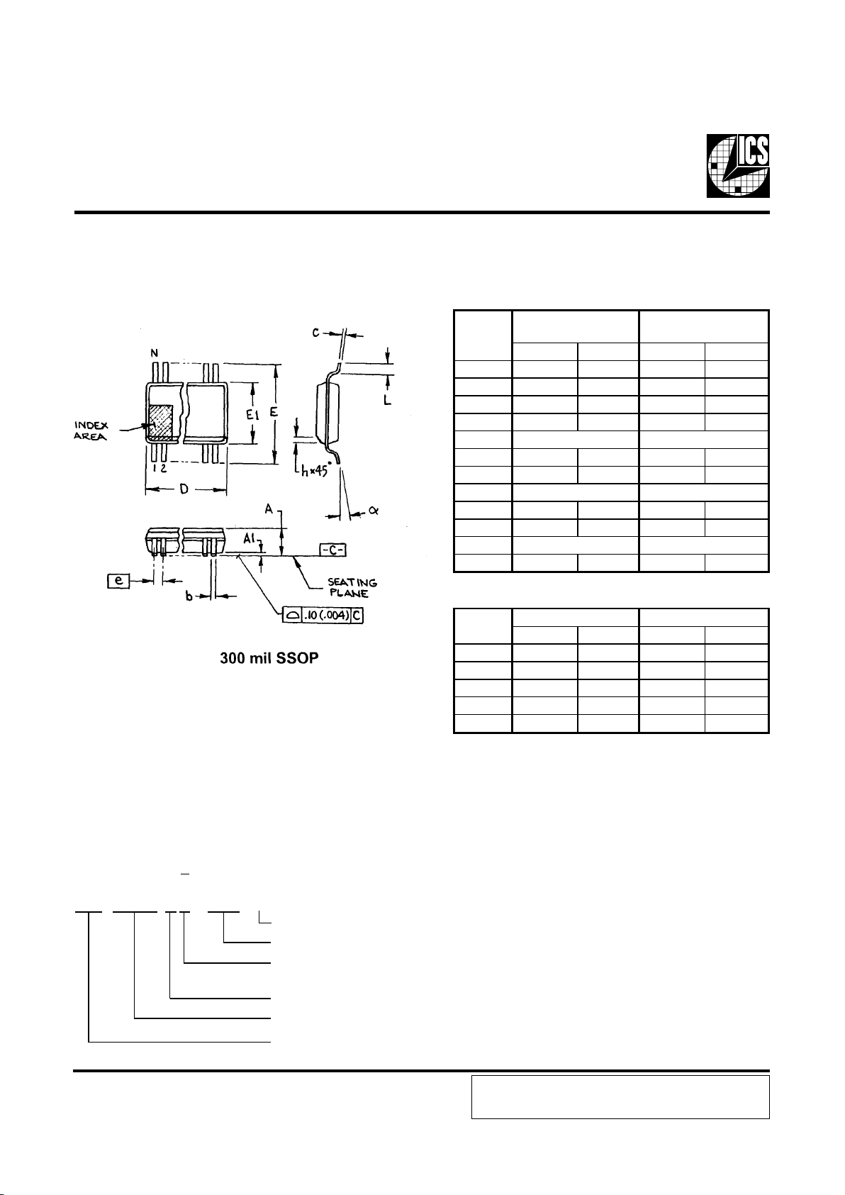
MIN MAX MIN MAX
A 2.413 2.794 .095 .110
A1 0.203 0.406 .008 .016
b 0.203 0.343 .008 .0135
c 0.127 0.254 .005 .010
D
E 10.033 10.668 .395 .420
E1 7.391 7.595 .291 .299
e 0.635 BASIC 0.025 BASIC
h 0.381 0.635 .015 .025
L 0.508 1.016 .020 .040
N
α
0° 8° 0° 8°
VARIATIONS
MIN MAX MIN MAX
28 9.398
9.652
.370 .380
34 11.303
11.557
.445 .455
48 15.748
16.002
.620 .630
56 18.288
18.542
.720 .730
64 20.828
21.082
.820 .830
SYM BO L
SEE VARIATI O NS
SEE VARIATI O NS
In Millimeters
COMMON DIMENSIONS
In Inches
COMMON DIMENSIONS
SEE VARIATIONS
N
D mm.
D (inch)
SEE VARIATIONS
ICS reserves the right to make changes in the device data identified in
this publication without further notice. ICS advises its customers to
obtain the latest version of all device data to verify that any
information being relied upon by the customer is current and accurate.
 Loading...