

Page 1
Integrated
Circuit
Systems, Inc.
ICS9248-128
Third party brands and names are the property of their respective owners.
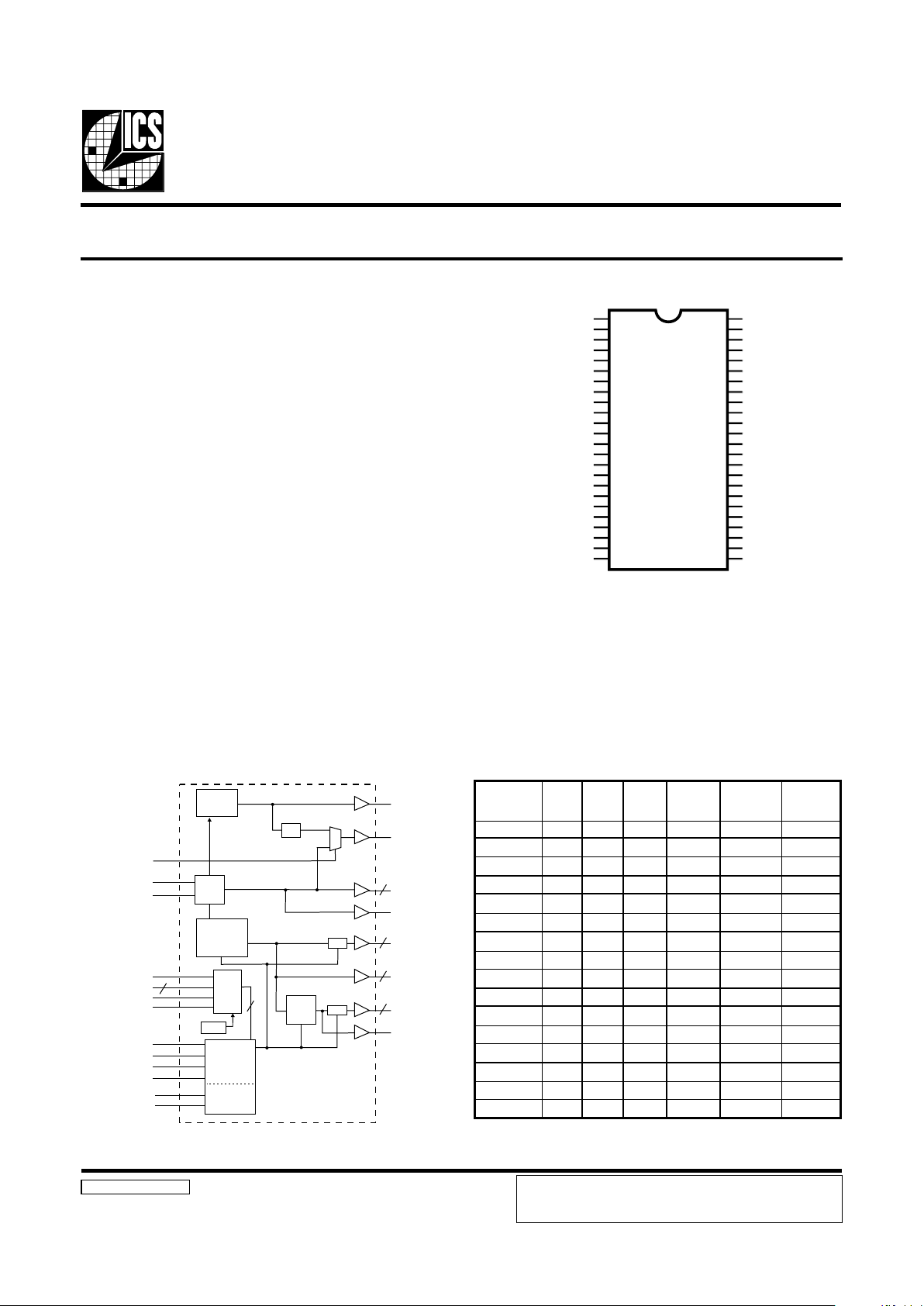
Block Diagram
9248-128 Rev B 11/16/00
Functionality
Pin Configuration
Recommended Application:
SIS 530/620 style chipset
Output Features:
• - 3 CPU @ 2.5V/3.3V up to 133.3 MHz.
• - 6 PCI @ 3.3V (including 1 free-running)
• - 13 SDRAMs @ 3.3V up to 133.3MHz.
• - 3 REF @ 3.3V , 14.318MHz
• - 1 clock @ 24/14.3 MHz selectable output for SIO
• - 1 Fixed clock at 48MHz (3.3V)
• - 1 IOAPIC @ 2.5V / 3.3V
Features:
• Up to 133MHz frequency support
• Support power management: CPU, PCI, SDRAM stop and
Power down Mode from I
2
C programming.
• Spread spectrum for EMI control ( ± 0.25% center spread
& 0 to -0.5% down spread).
• Uses external 14.318MHz crystal
• FS pins for frequency select
Key Specifications:
• CPU – CPU<175ps
• SDRAM – SDRAM < 350ps
• CPU–SDRAM < 500ps
• CPU(early) – PCI : 1-4ns (typ. 2ns)
• PCI – PCI <500ps
Frequency Generator & Integrated Buffers
VDDR/X
*MODE/REF0
GNDREF
X1
X2
VDDPCI
*FS1/PCICLK_F
*FS2.PCICLK0
GNDPCI
PCICLK1
PCICLK2
PCICLK3
PCICLK4
VDDPCI
SDRAM12
GNDSDR
*CPU_STOP# /SDRAM11
*PCI_STOP# /SDRAM10
VDDSD/C
*SDRAM_STOP# /SDRAM9
*PD# /SDRAM8
GNDFIX
SDATA
SCLK
VDDLAPIC
IOAPIC
REF1/SD_SEL#*
GNDLAPIC
REF2/CPU2.5_3.3#*
CPUCLK1
VDDLCPU
CPUCLK2
CPUCLK3
GNDCPU
SDRAM0
SDRAM1
VDDSDR
SDRAM2
SDRAM3
GNDSDR
SDRAM4
SDRAM5
VDDSDR
SDRAM6
SDRAM7
GNDSDR
48MHz/FS0*
SIO/SEL24_14#MHz
*
ICS9248-128
1
2
3
4
5
6
7
8
9
10
11
12
13
14
15
16
17
18
19
20
21
22
23
24
48
47
46
45
44
43
42
41
40
39
38
37
36
35
34
33
32
31
30
29
28
27
26
25
48-Pin SSOP
* Internal Pull-up Resistor of
120K to 3.3V on indicated inputs
CPU_STOP#
SDRAM_STOP#
PCI_STOP#
PD#
PLL2
PLL1
Spread
Spectrum
48MHz
SIO
REF(2:0)
IOAPIC
CPUCLK (3:1)
SDRAM (12:0)
PCICLK (4:0)
PCICLK_F
X1
X2
SEL24_14#
XTAL
OSC
PCI
CLOCK
DIVDER
STOP
STOP
SDATA
SCLK
MODE
FS(2:0)
CPU3.3#_2.5
SD_SEL#
Control
Logic
Config.
Reg.
LATCH
POR
PCI_STOP
CPU_STOP
3
3
13
5
5
3
/2
SD_SEL FS2 FS1 FS0
CPU
MHZ
SDRAM
MHZ
PCI
MHZ
0000
90.00 90.00 30.00
0 0 0 1 66.70 100.05 33.35
0 0 1 0 95.00 63.33 31.66
0 0 1 1 100. 00 66.66 33.33
0 1 0 0 100. 00 75.00 30.00
0 1 0 1 112. 00 74.66 37.33
0 1 1 0 124. 00 82.66 31.00
0 1 1 1 97.00 97.00 32.33
1 0 0 0 66.70 66.70 33.35
1 0 0 1 75.00 75.00 30.00
1 0 1 0 83.30 83.30 33.32
1 0 1 1 95.00 95.00 31.66
1 1 0 0 100. 00 100.00 33. 33
1 1 0 1 112. 00 112.00 37. 33
1 1 1 0 124. 00 124.00 31. 00
1 1 1 1 133. 30 133.30 33. 33
Note: REF , IOAPIC = 14.318MHz
ICS reserves the right to make changes in the device data identified in
this publication without further notice. ICS advises its customers to
obtain the latest version of all device data to verify that any
information being relied upon by the customer is current and accurate.
Page 2
2
ICS9248-128
Third party brands and names are the property of their respective owners.
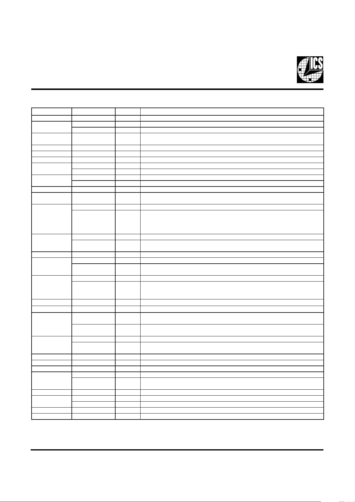
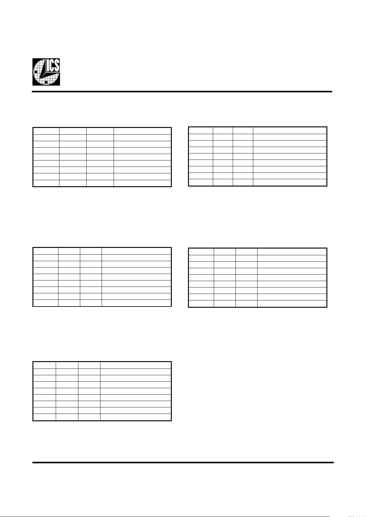
Pin Descriptions
Notes:
1: Internal Pull-up Resistor of 120K to 3.3V on indicated inputs
2: Bidirectional input/output pins, input logic levels are latched at internal power-on-reset. Use 10Kohm resistor
to program logic Hi to VDD or GND for logic low .
Pin number Pin name Type Description
1 VD DR/X P ower Is olat ed 3.3 V power for c rys tal & referenc e
RE F0 Outpu t 3.3V , 14.3 18 M Hz reference c loc k outpu t.
Mod e Input Fun ct ion s elec t pin, 1= des k to p m ode, 0= m obile m ode . Latc hed inpu t.
3,9,16, 22,
27,33,39
GND Pow er 3.3 V G round
4 X1 Input 14.3 18 M Hz c rys t al input
5 X2 Output 14.318 MHz c rys tal output
6,14 VD DP CI Power 3.3 V power for the P CI clo ck outp uts
FS1 Input Logic input frequency select bit. Input latched at power-on.
PC ICLK _F Out put 3.3 V free running PC I c loc k output, will not be s t opped by the P CI _S TO P #
PCICLK 0 Output 3.3 V PCI clock outputs, generating timing requirements for Pentium II
FS2 Input Logic input frequency select bit. Input latched at power-on.
13, 12, 11, 10 PC ICLK (4:1) Outpu t 3.3 V P CI c loc k ou tput s, generating tim ing requirem ents fo r Pent ium II
15,28,29,31,32,
34,35,37,38
SDRAM 12,
SDRA M (7:0)
Output SDRAM c lock outputs . F requency is s elected by S D-Sel latched input.
SDRA M 11 Output SDRAM c lock outputs . F requency is s elected by S D-Sel latched input.
CPU_S TOP # Input
As y nc h ronous ac tive low input pin us ed to stop the CP UCL K in low s tat e,
all other c loc k s will continue t o run. T he CP UCL K will h av e a " T urnon" lat enc y
of at least 3 CP U cloc k s.
SDRA M 10 Output SDRAM c lock outputs . F requency is s elected by S D-SE L latched input.
PCI-STOP# Input
Sy nc hronous ac tiv e low input us ed to s top t he P CICL K in a low st ate. It will not
effec t P CI CLK _F or any othe r outputs .
19 V DDS D/ C Pow er 3.3 V pow er for SDRA M out puts and c ore
SDRA M 9 Output SDRAM c lock outputs . F requency is s elected by S D-Sel latched input.
SDRAM_STOP# Input
As y nc h ronous ac tiv e low inpu t us ed to s t op t he S D RA M in a low s t ate.
It will no t ef fec t any ot her out puts .
SDRA M 8 Output SDRAM c lock outputs . F requency is s elected by S D-Sel latched input.
PD# Input
As y nc hronous ac tiv e low input pin us ed to pow er down the dev ic e into a low
power stat e. T he internal c loc k s are dis abled and t he V CO and the c rys t al are
st opped. Th e latenc y of t he pow er down will n ot b e greater than 3m s .
23 SDAT A Input
Data input for I
2
C serial input.
24 SC LK Input
Clock in put of I
2
C input
SEL24_14# Input
This input pin c ont rols th e frequenc y of the S I O. If logic 0 at power on
SI O= 14. 318 M Hz . If logic 1 at powe r-on SIO = 24M Hz .
SI O Out put Su per I/O ou tput . 24 or 14.318 M Hz . Se lect able at pow er-up by S E L24_14M Hz
FS0 Input Logic input frequency select bit. Input latched at power-on.
48 MH z Outpu t
3.3 V 48 M Hz c lock out put, fix ed frequenc y c loc k t ypic ally us ed wit h
USB devices
30,36 VDD S DR Pow er 3.3 V pow er for SDRA M out puts
40,41,4 3 CP UC LK (3:1) 0utput 2.5 V CP U and Hos t cloc k outpu ts
42 VD DLCP U P ower 2. 5 V po wer for CPU
RE F2 Outpu t 3.3V , 14.3 18 M Hz reference c loc k outpu t.
CP U3. 3#_2. 5 Input
This pin s elec ts the operat ing vo ltage for the CP U. If logic 0 at powe r on
CPU= 3.3 V and if logic 1 at power on CPU=2.5 V operating voltage.
45 GNDL Power 2.5 V Ground for the IOAPIC or CPU
RE F1 Outpu t 3.3V , 14.3 18 M Hz reference c loc k outpu t.
SD_ SE L # Input T his input pin c ont rols t he frequenc y of t he S DRA M .
47 IOA P IC Out put 2.5V fix ed 14.3 18 M Hz IO AP I C c loc k out puts
48 VDDLAPIC Power 2.5 V power for IOAP IC
2
1,2
8
1,2
26
1,2
7
1,2
46
1,2
44
1,2
17
1
20
1
18
1
21
1
25
1,2
Page 3
3
ICS9248-128
Third party brands and names are the property of their respective owners.
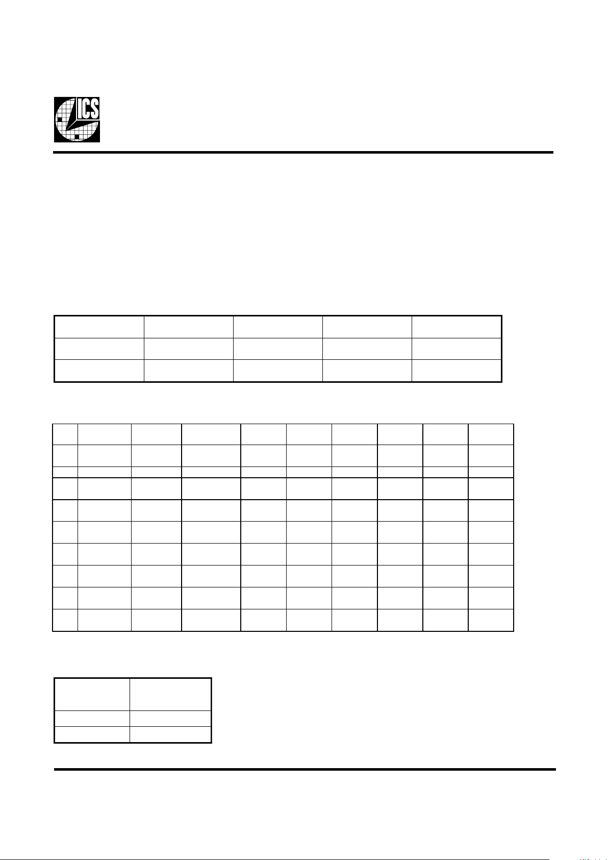
Power Management Functionality
Mode Pin - Power Management Input Control
CPU 3.3#_2.5V Buffer selector for CPUCLK drivers.
PD# CPU _ STOP# PCI_STOP# SDRA M_STOP
PCICLK
(0:4)
SDRAM
(0:12)
PCICLK_F CPUCLK
Crystal
OSC
VCO
0X X X
Stopped
Low
Stopped
Low
Stopped
Low
Stopped
Low
Stopped
Low
Stopped
Low
1 1 1 1 Running Running Running Running Running Running
1 1 1 0 Running
Stopped
Low
Running Running Running Running
11 0 1
Stopped
Low
Running Running Running Running Running
11 0 0
Stopped
Low
Stopped
Low
Running Running Running Running
1 0 1 1 Running Running Running
Stopped
Low
Running Running
1 0 1 0 Running
Stopped
Low
Running
Stopped
Low
Running Running
10 0 1
Stopped
Low
Running Running
Stopped
Low
Running Running
10 0 0
Stopped
Low
Stopped
Low
Running
Stopped
Low
Running Running
2niP,EDOM
)tupnIdehctaL(
71niP81niP02niP12niP
0
#POTS_UPC
)TUPNI(
#POTS_ICP
)TUPNI(
#POTS_MARDS
)TUPNI(
#DP
)TUPNI(
1
11MARDS
)TUPTUO(
01MARDS
)TUPTUO(
9MARDS
)TUPTUO(
8MARDS
)TUPTUO(
5.2_#3.3UPC
leveltupnI
)ataDdehctaL(
detceleSreffuB
:tanoitareporof
1DDVV5.2
0DDVV3.3
The ICS9248-128 is the single chip clock solution for Desktop/Notebook designs using the SIS style chipset. It provides all
necessary clock signals for such a system.
Spread spectrum may be enabled through I
2
C programming. Spread spectrum typically reduces system EMI by 8dB to 10dB.
This simplifies EMI qualification without resorting to board design iterations or costly shielding. The ICS9248-128 employs a
proprietary closed loop design, which tightly controls the percentage of spreading over process and temperature variations.
Serial programming I
2
C interface allows changing functions, stop clock programming and frequency selection. The SD_SEL
latched input allows the SDRAM frequency to follow the CPUCLK frequency(SD_SEL=1) or other clock frequencies
(SD_SEL=0)
General Description
Page 4
4
ICS9248-128
Third party brands and names are the property of their respective owners.
Byte 0: Functionality and frequency select register (Default = 0)
Serial Configuration Command Bitmap
Note 1: Default at power-up will be for latched logic inputs to define frequency .
I2C readback of the power up default indicates the revision ID code in bit 2, 6:4 as shown.
tiB
noitpircseD
DWP
7tiB
murtcepSdaerpSretneC%52.0±-0
1
murtcepSdaerpSnwoD%5.0-ot0-1
tiB
)4:6,2(
)4:6,2(tiBKLCUPCMARDSKLCICP
100,0
1etoN
000000.09
00.09
00.03
100007.66
50.001
53.33
010000.59
33.36
66.13
110000.001
66.66
33.33
001000.001
00.57
00.03
101000.211
66.47
33.73
011000.421
66.28
00.13
111000.79
00.79
33.23
000107.66
07.66
53.33
100100.57
00.57
00.03
010103.38
03.38
23.33
110100.59
00.59
66.13
001100.001
00.001
33.33
101100.211
00.211
33.73
011100.421
00.421
00.13
111103.331
03.331
33.33
3tiB
stupnidehctal,tceleserawdrahybdetcelessiycneuqerF-0
4:6,2tiBybdetcelessiycneuqerF-1
0
1tiB
lamroN-0
delbanemurtcepsdaerpS-1
1
0tiB
gninnuR-0
stuptuollaetatsirT-1
0
Page 5
5
ICS9248-128
Third party brands and names are the property of their respective owners.
Byte 1: CPU, Active/Inactive Register
(1 = enable, 0 = disable)
Byte 2: PCI Active/Inactive Register
(1 = enable, 0 = disable)
Byte 3: SDRAM Active/Inactive Register
(1 = enable, 0 = disable)
Notes:
1. Inactive means outputs are held LOW and are disabled
from switching.
Notes:
1. Inactive means outputs are held LOW and are disabled
from switching.
Notes:
1. Inactive means outputs are held LOW and are disabled
from switching.
Byte 4: SDRAM Active/Inactive Register
(1 = enable, 0 = disable)
Byte 5: Peripheral Active/Inactive Register
(1 = enable, 0 = disable)
Notes:
1. Inactive means outputs are held LOW and are disabled
from switching.
Notes:
1. Inactive means outputs are held LOW and are disabled
from switching.
tiB#niPDWPnoitpircseD
7tiB-1 )devreseR(
6tiB-1 )devreseR(
5tiB-1 )devreseR(
4tiB-1 )devreseR(
3tiB041 3KLCUPC
2tiB141 2KLCUPC
1tiB341 1KLCUPC
0tiB-X#0SF
tiB#niPDWPnoitpircseD
7tiB-X#1SF
6tiB71 F_KLCICP
5tiB-1 )devreseR(
4tiB311 4KLCICP
3tiB211 3KLCICP
2tiB111 2KLCICP
1tiB011 1KLCICP
0tiB81 0KLCICP
tiB#niPDWPnoitpircseD
7tiB821 7MARDS
6tiB921 6MARDS
5tiB131 5MARDS
4tiB231 4MARDS
3tiB431 3MARDS
2tiB531 2MARDS
1tiB731 1MARDS
0tiB831 0MARDS
tiB#niPDWPnoitpircseD
7tiB-1 )devreseR(
6tiB-X#2SF
5tiB-1 )devreseR(
4tiB741 CIPAOI
3tiB-X #LES_DS
2tiB4412FER
1tiB6411FER
0tiB210FER
tiB#niPDWPnoitpircseD
7tiB-1 )devreseR(
6tiB521 zHM41/42
5tiB621 zHM84
4tiB511 21MARDS
3tiB711 11MARDS
2tiB811 01MARDS
1tiB021 9MARDS
0tiB121 8MARDS
Page 6

6
ICS9248-128
Third party brands and names are the property of their respective owners.
Absolute Maximum Ratings
Supply Voltage . . . . . . . . . . . . . . . . . . . . . . . . . . . . 5.5 V
Logic Inputs . . . . . . . . . . . . . . . . . . . . . . . . . . . . . . GND –0.5 V to V
DD
+0.5 V
Ambient Operating Temperature . . . . . . . . . . . . . 0°C to +70°C
Storage Temperature . . . . . . . . . . . . . . . . . . . . . . . –65°C to +150°C
Case Temperature. . . . . . . . . . . . . . . . . . . . . . . . . . 115°C
Stresses above those listed under Absolute Maximum Ratings may cause permanent damage to the device. These ratings are
stress specifications only and functional operation of the device at these or any other conditions above those listed in the
operational sections of the specifications is not implied. Exposure to absolute maximum rating conditions for extended periods
may affect product reliability.
Electrical Characteristics - Input/Supply/Common Output Parameters
TA = 0 - 70C; Supply Voltage VDD = V
DDL
= 3.3 V +/-5% (unless otherwise stated)
PARAMETER SYMBOL CONDITIONS MIN TYP MAX UNITS
Input High Voltage V
IH
2V
DD
+0.3 V
Input Low Voltage V
IL
VSS-0.3 0.8 V
Input High Current I
IH
V
I
N
= V
DD
5
µ
A
Input Low Current I
IL1
V
I
N
= 0V; Inputs with no pull-up resistors -5
µ
A
Input Low Current I
IL2
V
I
N
= 0V; Inputs with pull-up resistors -200
µ
A
I
DD3.3OP66
CL = 0 pF; Select @ 66 MHz 150 180 mA
I
DD3.3OP100
CL = 0 pF; Select @ 100 MHz 170 180 mA
Powerdown Current
I
DD3.3PD
CL = 0 pF; Input address to VDD or GND
2
606
00
µ
A
Input Frequency F
i
VDD = 3.3 V 11 14.318 16 MHz
C
I
N
Logic Inputs 5
p
F
C
INX
X1 & X2 pins 27 45
p
F
Transition time
1
T
trans
To 1st crossing of target frequenc
y
3ms
Clk Stabiliz ation
1
T
STAB
From VDD = 3.3 V to 1% target frequenc
y
3ms
T
CPU100SDRAM100
VT = 1.5V 300 500
p
s
Skew
1
T
CPU-PCI
VT = 1.5V
12.6 4 ns
1
Guaranteed by design, not 100% tested in production.
Input Capacitance
1
Operating Supply
Current
Electri cal Charact eristics - Input/Suppl y/Common O utput Param eters
TA = 0 - 70C ; Supply Voltage VDD = 3.3 V +/- 5%, V
DDL
= 2.5V +/ - 5% (unle ss other wise stated).
PARAME TE R SY MBOL CONDITIONS MIN TYP MAX UNITS
I
DD2.5OP66
CL = 0 pF; Selec t @ 66 MHz
60 72 mA
I
DD2.5OP100
CL = 0 pF; Selec t @ 100 MHz
80 100 mA
T
CPU100SDRAM100VT
= 1.5V; VTL = 1.25V 230 500 ps
T
CPU-PCI
VT = 1.5V; VTL = 1.25V
12.6 4 ns
1
Guara nt e e d by de sign, not 100% tested i n producti on.
Operating Supply
Current
Skew
1
Page 7

7
ICS9248-128
Third party brands and names are the property of their respective owners.
El e ctrical Characterist ics - CPUCLK
TA = 0 - 70º C; VDD = V
DDL
= 3.3 V + / -5%; CL = 10 - 20 pF ( unl e ss otherwise stated) .
PARAMETER SYMBOL CONDITIONS MIN TYP MAX UNITS
Out put High Voltage V
OH2B
IOH = -12 mA 2. 4 2.2 V
Output Low Voltage V
OL2B
IOL = 12 mA 0.3 0.4 V
Out put High Current I
OH2B
VOH = 2 V -16 -19
mA
Out put Low Cur rent I
OL2B
VOL = 0.8 V 19 22
mA
Rise Time t
r2B
1
VOL = 0.4 V, VOH = 2.4 V 1.45 2 ns
Fall Time t
f2B
1
VOH = 2.4 V, VOL = 0.4 V 0.95 2 ns
Duty Cycle d
t2B
1
VT = 1.5 V 45 46 55 %
Skew
t
sk2B
1
VT = 1.5 V 65 175 ps
Jitter, Cycle-to-cycle
t
jcyc-cyc2B
1
VT = 1.5 V @ CPU & SDRA M = 100 MHz
210 250 ps
1
Gua ranteed by de sign, not 100% tested in pr oduc tion.
El e ctrical Characteristics - C PUCLK
TA = 0 - 70º C; VDD = 3.3 V +/-5%, V
DDL
= 2.5V + / - 5 %; CL = 10 - 20 pF ( unl e ss otherwise stated).
PARAMETER SYMBOL CONDITIONS MIN TYP MAX UNITS
Output High Voltage V
OH2B
IOH = -12 mA 2 2.2 V
Output Low Voltage V
OL2B
IOL = 12 mA 0.25 0.4 V
Out put High Current I
OH2B
VOH = 1.7 V -15 - 19
mA
Output Low Current I
OL2B
VOL = 0.7 V 19 23
mA
Rise Time t
r2B
1
VOL = 0.4 V, VOH = 2.0 V 1.4 1.6 ns
Fall Time t
f2B
1
VOH = 2.0 V, VOL = 0.4 V 1.2 1.6 ns
Duty Cycle d
t2B
1
VT = 1.25 V 45 48 55 %
Skew
t
sk2B
1
VT = 1.25 V 50 175 ps
Jitter, Cycle-to-cycle
t
jcyc-cyc2B
1
VT = 1.25 V @ CPU &
SDRAM = 100 MHz
210 250 ps
1
Gua ranteed by de sign, not 100% te sted in produc t i on.
Page 8

8
ICS9248-128
Third party brands and names are the property of their respective owners.
El e ctrical Characterist ics - PCICLK
TA = 0 - 70º C; VDD = 3.3 V +/- 5%, V
DDL
= 2.5 V + / - 5 %; CL = 30 pF (unless other wise stated) .
PARAMETER SYMBOL CONDITIONS MIN TYP MAX UNITS
Out put High Voltage V
OH1
IOH = -11 mA 2. 4 2.6 V
Output Low Voltage V
OL1
IOL = 9.4 mA 0.3 0.4 V
Out put High Current I
OH1
VOH = 2.0 V -18 22
mA
Out put Low Cur rent I
OL1
VOL = 0.8 V 16 24
mA
Rise Time t
r1
1
VOL = 0.4 V, VOH = 2.4 V 1.8 2 ns
Fall Time t
f1
1
VOH = 2.4V, VOL = 0.4 V 1.7 2 ns
Duty Cycle d
t1
1
VT = 1.5 V 45 49 55 %
Skew
t
sk1
1
VT = 1.5 V 260 500 ps
Jitter, Cycle-to-cycle
t
jcyc-cyc
1
VT = 1.5 V
150 500 ps
1
Gua ranteed by de sign, not 100% tested in pr oduc tion.
El e ctrical Characteristics - SDRAM
TA = 0 - 70º C; VDD = 3.3 V +/- 5%, V
DDL
= 2.5 V + / - 5 %; CL = 30 pF (unless other wise stated) .
PARAMETER SYMBOL CONDITIONS MIN TYP MAX UNITS
Out put High Voltage V
OH1
IOH = -11 mA 2. 4 2.6 V
Output Low Voltage V
OL1
IOL = 9.4 mA 0.3 0.4 V
Out put High Current I
OH1
VOH = 2.0 V -18 22
mA
Out put Low Cur rent I
OL1
VOL = 0.8 V 16 24
mA
Rise Time t
r1
1
VOL = 0.4 V, VOH = 2.4 V 1.6 2 ns
Fall Time t
f1
1
VOH = 2.4V, VOL = 0.4 V 1.6 2 ns
d
t1
1
VT = 1.5 V; divide by 2 selects < 124 MHz47 50 57 %
d
t2
1
VT = 1.5 V; divide by 3 selects 45 50 55 %
d
t3
1
VT = 1.5 V; selects >= 124 MHz 43 50 53 %
t
sk1
1
VT = 1.5 V; S DRAM 8, 9, 11 & 12 110 250 ps
t
sk2
1
VT = 1.5 V; all e xcept SDRAM 8, 9, 11 & 12 100 250 ps
t
sk3
1
VT = 1.5 V; all SDRAMs 220 350 ps
Jitter, Cycle-to-cycle
t
jcyc-cyc
1
VT = 1.5 V
200 500 ps
1
Gua ranteed by de sign, not 100% tested in pr oduc tion.
Skew
Duty Cycle
Page 9

9
ICS9248-128
Third party brands and names are the property of their respective owners.
El e ctrical Characterist ics - REF/48MHz/SIO
TA = 0 - 70º C; VDD = 3.3 V +/- 5%, V
DDL
= 2.5 V + / - 5 %; CL = 20 pF (unless other wise stated) .
PARAMETER SYMBOL CONDITIONS MIN TYP MAX UNITS
Output High
Voltage
V
OH5
IOH = -12 mA 2. 4 2.6 V
Output Low Voltage V
OL5
IOL = 10 mA 0.3 0.4 V
Out put High Current I
OH5
VOH = 2.0 V -18 22
mA
Out put Low Current I
OL5
VOL = 0.8 V 16 24
mA
Rise Ti m e
t
r5
1
VOL = 0.4 V, VOH = 2.4 V 2.1 4 ns
Fall Time
t
f5
1
VOH = 2.4V, VOL = 0.4 V 2.1 4 ns
Duty Cycle
d
t5
1
VT = 1.5 V 45 51 55 %
Jitter, Cycle-to-
Cycle, REF
t
jcyc -cyc, REF
1
VT = 1.5 V 600 1000 ps
Jitter, Cycle-to-
C ycle, fixed clock
t
jcyc -cyc, fixed
1
VT = 1.5 V 400 500 ps
1
Gua ranteed by de sign, not 100% tested in pr oduc tion.
Page 10

10
ICS9248-128
Third party brands and names are the property of their respective owners.
1. The ICS clock generator is a slave/receiver, I2C component. It can read back the data stored in the latches for
verification. Read-Back will support Intel PIIX4 "Block-Read" protocol.
2. The data transfer rate supported by this clock generator is 100K bits/sec or less (standard mode)
3. The input is operating at 3.3V logic levels.
4. The data byte format is 8 bit bytes.
5. To simplify the clock generator I
2
C interface, the protocol is set to use only "Block-Writes" from the controller. The
bytes must be accessed in sequential order from lowest to highest byte with the ability to stop after any complete byte
has been transferred. The Command code and Byte count shown above must be sent, but the data is ignored for those
two bytes. The data is loaded until a Stop sequence is issued.
6. At power-on, all registers are set to a default condition, as shown.
General I2C serial interface information
The information in this section assumes familiarity with I2C programming.
For more information, contact ICS for an I
2
C programming application note.
How to Write:
• Controller (host) sends a start bit.
• Controller (host) sends the write address D2
(H)
• ICS clock will acknowledge
• Controller (host) sends a dummy command code
• ICS clock will acknowledge
• Controller (host) sends a dummy byte count
• ICS clock will acknowledge
• Controller (host) starts sending first byte (Byte 0)
through byte 5
• ICS clock will acknowledge each byte one at a time.
• Controller (host) sends a Stop bit
How to Read:
• Controller (host) will send start bit.
• Controller (host) sends the read address D3
(H)
• ICS clock will acknowledge
• ICS clock will send the byte count
• Controller (host) acknowledges
• ICS clock sends first byte (Byte 0) through byte 6
• Controller (host) will need to acknowledge each byte
• Controller (host) will send a stop bit
Notes:
Controller (Host) ICS (Slave/Receiver)
Start Bit
Address
D2
(H)
A
CK
Dummy Command Code
A
CK
Dummy Byte Count
ACK
Byte 0
A
CK
Byte 1
A
CK
Byte 2
ACK
Byte 3
A
CK
Byte 4
A
CK
Byte 5
ACK
Byte 6
A
CK
Stop Bit
How to Write:
Controller (Host) ICS (Slave/Receiver)
Start Bit
Address
D3
(H)
A
CK
Byte Count
ACK
Byte 0
ACK
Byte 1
ACK
Byte 2
ACK
Byte 3
ACK
Byte 4
ACK
Byte 5
ACK
Byte 6
ACK
Stop Bit
How to Read:
Page 11

11
ICS9248-128
Third party brands and names are the property of their respective owners.
CPU_STOP# Timing Diagram
CPU_STOP# is an asychronous input to the clock synthesizer. It is used to turn off the CPU clocks for low power operation.
CPU_STOP# is synchronized by the ICS9248-128. The minimum that the CPU clock is enabled (CPU_STOP# high pulse) is
100 CPU clocks. All other clocks will continue to run while the CPU clocks are disabled. The CPU clocks will always be stopped
in a low state and start in such a manner that guarantees the high pulse width is a full pulse. CPU clock on latency is less than
4 CPU clocks and CPU clock off latency is less than 4 CPU clocks.
Notes:
1. All timing is referenced to the internal CPU clock.
2. CPU_STOP# is an asynchronous input and metastable conditions may exist. This signal is synchronized
to the CPU clocks inside the ICS9248-128.
3. All other clocks continue to run undisturbed. (including SDRAM outputs).
Page 12

12
ICS9248-128
Third party brands and names are the property of their respective owners.
SDRAM_STOP# Timing Diagram
SDRAM_STOP# is an sychronous input to the clock synthesizer. It is used to turn off the CPU clocks for low power operation.
SDRAM_STOP# is synchronized by the ICS9248-128. All other clocks will continue to run while the SDRAM clocks are
disabled. The SDRAM clocks will always be stopped in a low state and start in such a manner that guarantees the high pulse
width is a full pulse.
Notes:
1. All timing is referenced to the internal CPU clock.
2. SDRAM is an asynchronous input and metastable conditions may exist. This signal is synchronized to
the SDRAM clocks inside the ICS9248-128.
3. All other clocks continue to run undisturbed.
Page 13

13
ICS9248-128
Third party brands and names are the property of their respective owners.
PCI_STOP# Timing Diagram
PCI_STOP# is an synchronous input to the ICS9248-128. It is used to turn off the PCICLK (0:4) clocks for low power operation.
PCI_STOP# is synchronized by the ICS9248-128 internally. The minimum that the PCICLK (0:4) clocks are enabled (PCI_STOP#
high pulse) is at least 10 PCICLK (0:4) clocks. PCICLK (0:4) clocks are stopped in a low state and started with a full high pulse
width guaranteed. PCICLK (0:4) clock on latency cycles are only one rising PCICLK clock off latency is one PCICLK clock.
Notes:
1. All timing is referenced to the Internal CPUCLK (defined as inside the ICS9248 device.)
2. PCI_STOP# is an asynchronous input, and metastable conditions may exist. This signal is required to be synchronized
inside the ICS9248.
3. All other clocks continue to run undisturbed.
4. CPU_STOP# is shown in a high (true) state.
Page 14

14
ICS9248-128
Third party brands and names are the property of their respective owners.
Fig. 1
Shared Pin Operation Input/Output Pins
The I/O pins designated by (input/output) on the ICS9248128 serve as dual signal functions to the device. During initial
power-up, they act as input pins. The logic level (voltage)
that is present on these pins at this time is read and stored
into a 5-bit internal data latch. At the end of Power -On reset,
(see AC characteristics for timing values), the device changes
the mode of operations for these pins to an output function.
In this mode the pins produce the specified buffered clocks
to external loads.
T o program (load) the internal configuration register for these
pins, a resistor is connected to either the VDD (logic 1) power
supply or the GND (logic 0) voltage potential. A 10 Kilohm
(10K) resistor is used to provide both the solid CMOS
programming voltage needed during the power-up
programming period and to provide an insignificant load on
the output clock during the subsequent operating period.
Via to
VDD
Clock trace to load
Series Term. Res.
Programming
Header
Via to Gnd
Device
Pad
2K
8.2K
Figure 1 shows a means of implementing this function when
a switch or 2 pin header is used. W ith no jumper is installed
the pin will be pulled high. W ith the jumper in place the pin
will be pulled low. If programmability is not necessary, than
only a single resistor is necessary . The programming resistors
should be located close to the series termination resistor to
minimize the current loop area. It is more important to locate
the series termination resistor close to the driver than the
programming resistor.
Page 15

15
ICS9248-128
Third party brands and names are the property of their respective owners.
General Layout Precautions:
1) Use a ground plane on the top layer
of the PCB in all areas not used by
traces.
2) Make all power traces and ground
traces as wide as the via pad for lower
inductance.
Notes:
1) All clock outputs should have a
series terminating resistor, and a 20pF
capacitor to ground between the
resistor and clock pin. Not shown in
all places to improve readibility of
diagram.
2) Optional crystal load capacitors are
recommended. They should be
included in the layout but not
inserted unless needed.
Connections to VDD:
C1
C1
C4
1
Clock Load
C3
C3
48
47
46
45
44
43
42
41
40
39
38
37
36
35
34
33
32
31
30
29
28
27
26
25
1
2
3
4
5
6
7
8
Ferrite
Bead
VDD
C2
22µF/20V
Tantalum
Ferrite
Bead
VDD
C2
22µF/20V
Tantalum
1
2
3
4
5
6
7
8
9
10
11
12
13
14
15
16
17
18
19
20
21
22
23
24
= Routed Power
= Ground Connection Key (component side copper)
= Ground Plane Connection
= Power Route Connection
= Solder Pads
= Clock Load
Ground
2.5V Power Route
3.3V Power Route
3.3V Power Route
Page 16

16
ICS9248-128
Third party brands and names are the property of their respective owners.
Ordering Information
ICS9248yF-128
Pattern Number (2 or 3 digit number for parts with ROM code patterns)
Package Type
F=SSOP
Revision Designator
Device Type (consists of 3 or 4 digit numbers)
Prefix
ICS, AV = Standard Device
Example:
ICS XXXX y F - PPP
MIN MAX MIN MAX
A 2.413 2.794 .095 .110
A1 0.203 0.406 .008 .016
b 0.203 0.343 .008 .0135
c 0.127 0.254 .005 .010
D
E 10.033 10.668 .395 .420
E1 7.391 7.595 .291 .299
e 0.635 BASIC 0.025 BASIC
h 0.381 0.635 .015 .025
L 0.508 1.016 .020 .040
N
α
0° 8° 0° 8°
VARIATIONS
MIN MAX MIN MAX
48 15.748 16.002 .620 .630
JEDEC MO-118
DOC# 10-0034
6/1/00
REV B
N
D mm.
D (inch)
SEE VARIATIONS
SYMBOL
SEE VARIATIONS
SEE VARIATIONS
In Millimeters
COMMON DIMENSIONS
In Inches
COMMON DIMENSIONS
SEE VARIATIONS
ICS reserves the right to make changes in the device data identified in
this publication without further notice. ICS advises its customers to
obtain the latest version of all device data to verify that any
information being relied upon by the customer is current and accurate.
 Loading...