

Page 1
Integrated
Circuit
Systems, Inc.
ICS9248-110
Third party brands and names are the property of their respective owners.
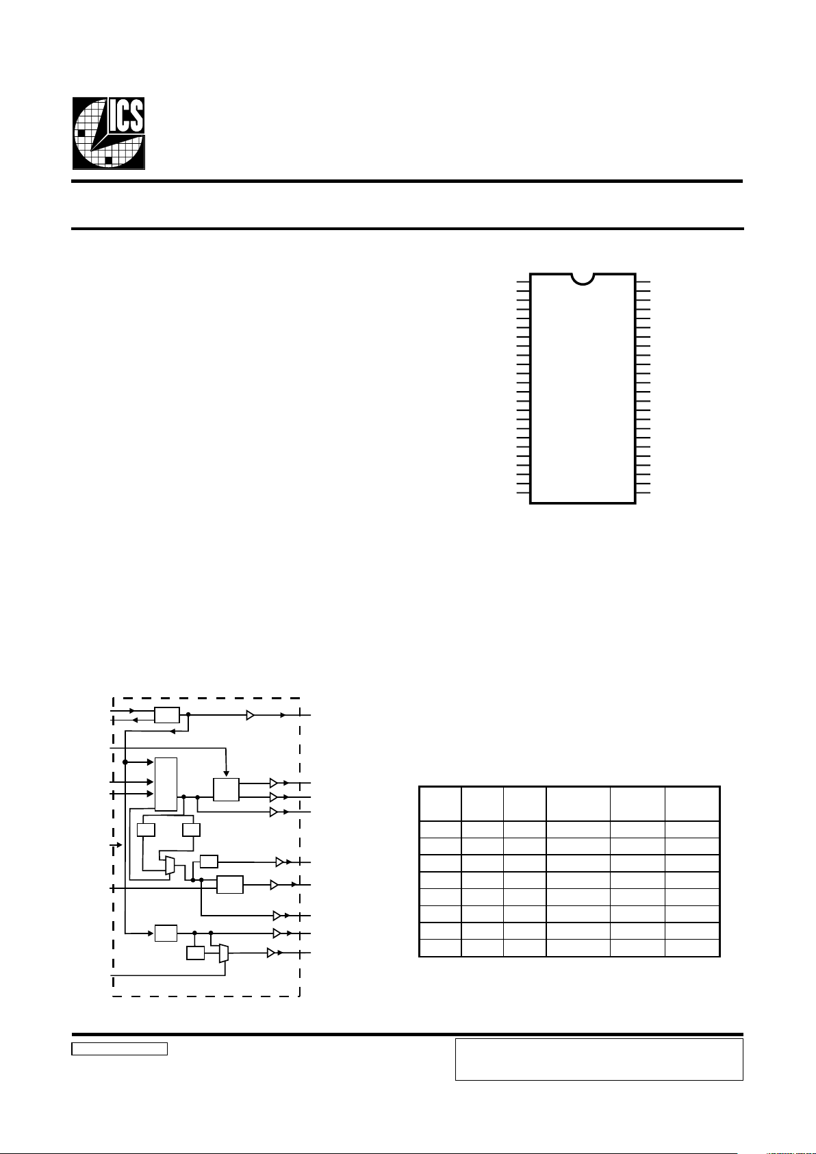
Block Diagram
9248-110 Rev C 01/08/01
Functionality
Pin Configuration
48-Pin 300mil SSOP
Recommended Application:
AMD-K7 based systems
Output Features:
• 3 differential pair open drain CPU clocks (2.7V external
pull-up; up to 150MHz achieviable through I
2
C)
• 2 - AGPCLK @ 3.3V
• 8 - PCI @3.3V, including 1 free running
• 1 - 48MHz @ 3.3V
• 1 - 24/48MHz @ 3.3V
• 2- REF @3.3V, 14.318MHz.
Features:
• Up to 150MHz frequency support
• Support power management: CPU, PCI, stop and Power
down Mode from I
2
C programming.
• Spread spectrum for EMI control -0.5% down spread
• Uses external 14.318MHz crystal
• FS pins for frequency select
Key Specifications:
• CPU – CPU: <250ps
• AGP-AGP: <250ps
• PCI – PCI: <400ps
• CPU - SDRAM_OUT: <400ps
• CPU-AGP <250ps
AMD-K7TM System Clock Chip
* Internal 120K pullup resistor on indicated inputs
** Internal 240K pullup resistor on indicated inputs
**FS0/REF0
**FS1/REF1
GNDREF
X1
X2
GNDPCI
PCICLK_F
PCICLK0
VDDPCI
PCICLK1
PCICLK2
GNDPCI
PCICLK3
PCICLK4
VDDPCI
PCICLK5
PCICLK6
VDDAGP
AGP0
AGP1
GNDAGP
VDD48
48MHz
SEL24_48#/24-48MHz
VDDREF
GNDSD
SDRAM_OUT
VDDSD
RESERVED
CPUCLKC2
CPUCLKT2
GNDCPU
CUCLKC1
CPUCLKT1
GND
CPUCLKC0
CPUCLKT0
RESERVED
VDD
GND
PCI_STOP#
CPU_STOP
PD#
SPREAD#
FS2*
S DATA
SCLK
GND48
ICS9248-110
1
2
3
4
5
6
7
8
9
10
11
12
13
14
15
16
17
18
19
20
21
22
23
24
48
47
46
45
44
43
42
41
40
39
38
37
36
35
34
33
32
31
30
29
28
27
26
25
FS (2:0)
SPREAD#
CPU_STOP#
X1
X2
OSC
PLL
CPU
STOP
PLL2
REF (1:0)
CPUCLKC (2:0)
CPUCLKT (2:0)
SDRAM_OUT
48MHz
PCICLK (6:0)
24_48MHz
PCICLK_F
PCI_STOP#
SEL24_48#
PD#
/ 2 / 3
PCI
STOP
X 2
/ 2
AGP (1:0)
0 0 0 90 30.00 60.00
0 0 1 95 31.67 63.33
0 1 0 100.99 33.66 67.33
0 1 1 115 38.33 76.67
1 0 0 100.7 33.57 67.13
1 0 1 103 34.33 68.67
1 1 0 105 35.00 70.00
1 1 1 110 36.67 73.33
PCI AGPFS2 FS1 FS0
CPU,
SDRAM
ICS reserves the right to make changes in the device data identified in
this publication without further notice. ICS advises its customers to
obtain the latest version of all device data to verify that any
information being relied upon by the customer is current and accurate.
Page 2
2
ICS9248-110
Third party brands and names are the property of their respective owners.
Pin Descriptions
REBMUNNIPEMANNIPEPYTNOITPIRCSED
1,2
)0:1(SFNIDDVotpu-llupsah,sniptceleSycneuqerF
)0:1(FERTUOtuptuokcolczHM813.41
3FERDNGRWPstuptuoFERrofdnuorG
41XNI
daolFp33lanretnisah,tupnilatsyrCzHM813.41NI_LATX
2Xmorfrotsiserkcabdeefdnapac
52XTUOFp33pacdaollanretnisah,tuptuolatsyrCTUO_LATX
21,6ICPDNGRWPstuptuoICProfdnuorG
7F_KLCICPTUO
#POTS_ICPehtybdetceffatoN.tuptuoICPgninnuReerF
.tupni
8,01,11,31,41,61,71)0:6(KLCICPTUOV3.3elbitapmocLTT.stuptuokcolcICP
51,9ICPDDVRWPV3.3yllanimon,stuptuoKLCICProfrewoP
81PGADDVRWPV3.3yllanimon,stuptuoPGArofrewoP
91,02)0:1(PGATUO.deppotsebtonyamesehT.ICPX2sadenifedstuptuoPGA
12PGADNGRWPstuptuokcolcPGArofdnuorG
43DDVRWPV3.3yllanimon,erocrofrewopdetalosI
33DNGRWPerocrofdnuorgdetalosI
2284DDVRWPV3.3yllanimonstuptuoCDF,BSUrofrewoP
32zHM84TUOtuptuozHM84
42
#84-42LESNI
42niproftuptuozHM84ro42stceleS
zHM42=hgiHzHM84=woL
zHM84-42TUO#84-42LEShguorhtelbatcelestuokcolcdexiF
5284DNGRWPstuptuozHM84rofdnuorG
62KLCSNIIroftupnikcolC
2
C
72ATADSO/IIrofnipataD
2
tnarelotV5yrtiucricC
822SFNIDDVotpu-llupsah,niptceleSycneuqerF
92#DAERPSNI
daerpSnwoD.WOLnehwerutaefmurtcepSdaerpSselbanE
zHK05=ycneuqerfnoitaludom%5.0
03#DPNI
erastuptuolla&LLPlanretnI.wolevitca,pihcnwodsrewoP
.delbasid
13#POTS_UPCNI
CKLCUPCsarehwWOLnevirdsTKLCUPC.sKLCUPCstlaH
detressasinipsihtnehwHGIHnevirdsi
.)WOLevitcA(
23#POTS_ICPNI
F_KLCICP.wolnevirdnehwlevel"0"cigoltasuBICPstlaH
nipsihtybdetceffatonsi
64TUO_MARDSTUOreffubyaledorezMARDSrofkcolcecnerefeR
43DDVRWPerocrofrewopdetalosI
44,53DEVRESERC/NliarrewopUPCerutruF
63,93,24)0:2(TKLCUPCTUO
nepoesehT.stuptuoUPCriaplaitnereffidfoskcolc"eurT"
.pu-llupV5.1lanretxenadeenstuptuoniard
73,04,34)0:2(CKLCUPCTUO
esehT.tuptuoUPCriaplatnereffidfoskcolc"yrotnemelpmoC"
.pu_llupV5.1lanretxenadeenstuptuoniardnepo
14,83UPCDNGRWP.stuptuoKLCUPCrofdnuorG
54DSDDVRWPV3.3yllanimoN.nipTUO_MARDSrofrewoP
74DSDNGRWPsnipTUO_MARDSrofdnuorG
84FERDDVRWPV3.3yllanimon,2X,1X,FERrofrewoP
Page 3
3
ICS9248-110
Third party brands and names are the property of their respective owners.
General Description
The ICS9248-110 is a main clock synthesizer chip for AMD-K7 based systems. This provides all clocks required for such a
system when used with a Zero Delay Buffer Chip such as the ICS9179-06.
Spread spectrum may be enabled through I
2
C programming. Spread spectrum typically reduces system EMI by 8dB to
10dB. This simplifies EMI qualification without resorting to board design iterations or costly shielding. The ICS9248-110
employs a proprietary closed loop design, which tightly controls the percentage of spreading over process and temperature
variations.
Serial programming I
2
C interface allows changing functions, stop clock programming and frequency selection.
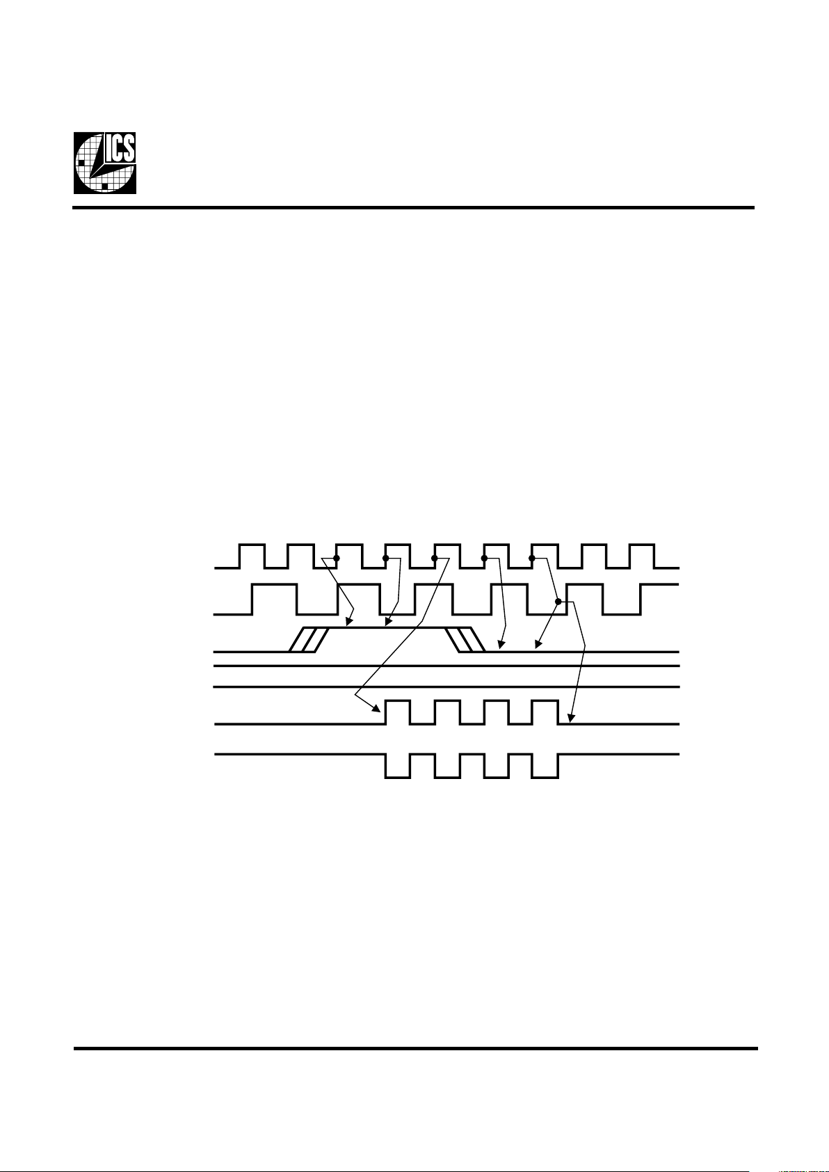
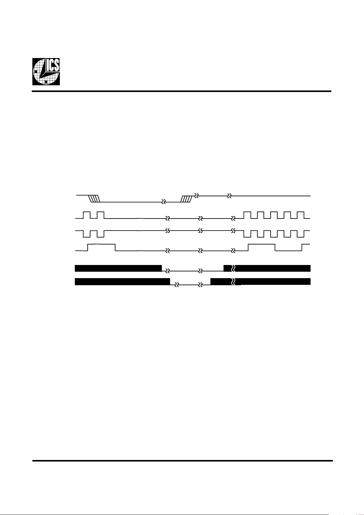
CPU_STOP# Timing Diagram
CPU_STOP# is an asychronous input to the clock synthesizer. It is used to turn off the CPUCLKs for low power operation.
CPU_STOP# is synchronized by the ICS9248-110. All other clocks will continue to run while the CPUCLKs clocks are
disabled. The CPUCLKs will always be stopped in a low state and start in such a manner that guarantees the high pulse width
is a full pulse. CPUCLK on latency is less than 4 CPUCLKs and CPUCLK off latency is less than 4 CPUCLKs.
Notes:
1. All timing is referenced to the internal CPUCLK.
2. CPU_STOP# is an asynchronous input and metastable conditions may exist. This signal is
synchronized to the CPUCLKs inside the ICS9248-110.
3. All other clocks continue to run undisturbed.
4. PD# and PCI_STOP# are shown in a high (true) state.
PCICLK
CPUCLKT
CPUCLKC
PCI_STOP# (High)
CPU_STOP#
PD# (High)
INTERNAL
CPUCLK
Page 4
4
ICS9248-110
Third party brands and names are the property of their respective owners.
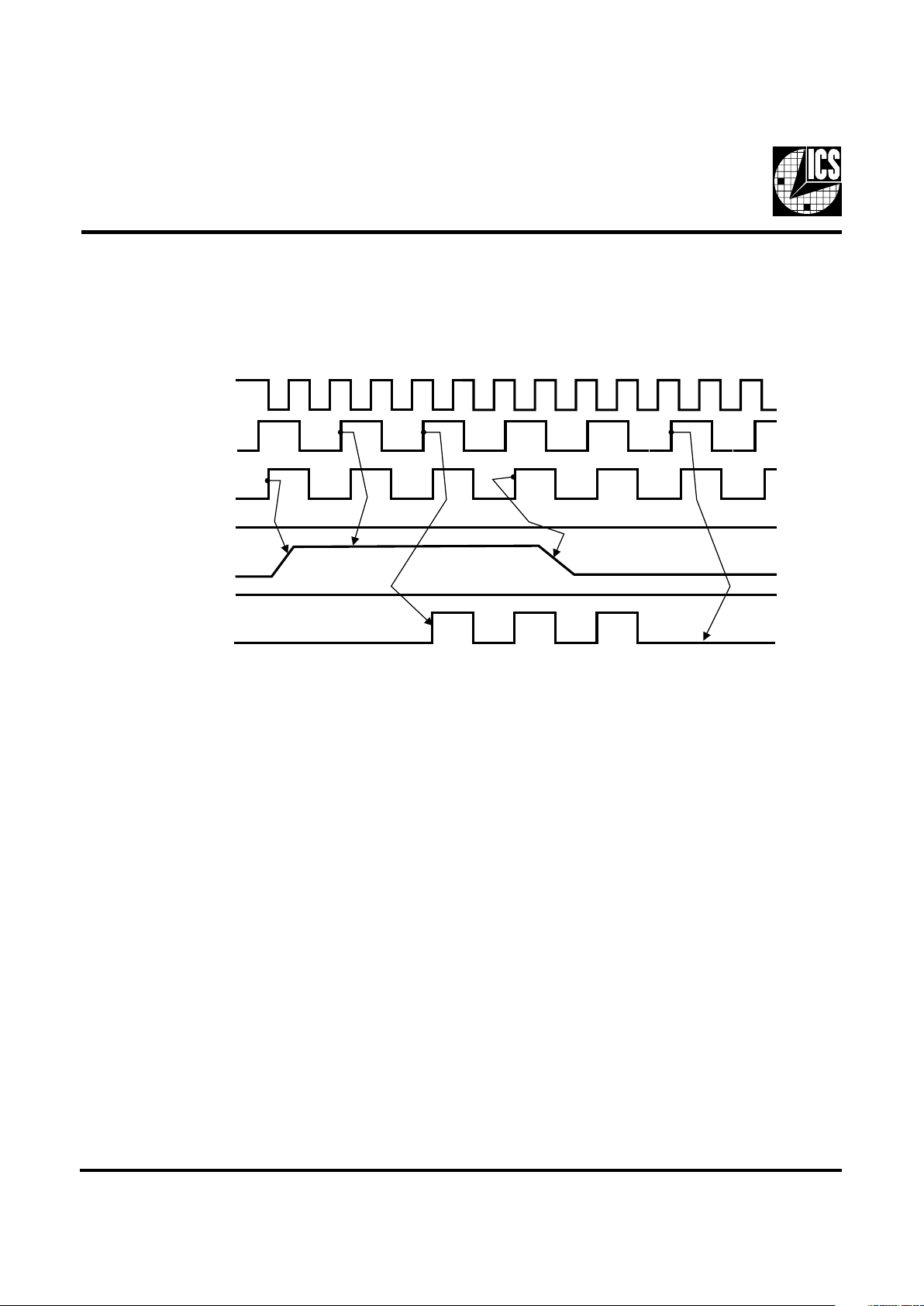
PCI_STOP# Timing Diagram
PCI_STOP# is an asynchronous input to the ICS9248-110. It is used to turn off the PCICLK (0:5) clocks for low power
operation. PCI_STOP# is synchronized by the ICS9248-110 internally. PCICLK (0:5) clocks are stopped in a low state and
started with a full high pulse width guaranteed. PCICLK (0:5) clock on latency cycles are only one rising PCICLK clock off
latency is one PCICLK clock.
Notes:
1. All timing is referenced to the Internal CPUCLK (defined as inside the ICS9248 device.)
2. PCI_STOP# is an asynchronous input, and metastable conditions may exist. This signal is required to be synchronized
inside the ICS9248.
3. All other clocks continue to run undisturbed.
4. PD# and CPU_STOP# are shown in a high (true) state.
CPUCLK
(Internal)
PCICLK
(Internal)
PCICLK
(Free-runningl)
CPU_STOP#
PWR_DWN#
PCICLK
(External)
PCI_STOP#
Page 5
5
ICS9248-110
Third party brands and names are the property of their respective owners.
PD# Timing Diagram
The power down selection is used to put the part into a very low power state without turning off the power to the part. PD# is
an asynchronous active low input. This signal needs to be synchronized internal to the device prior to powering down the
clock synthesizer.
Internal clocks are not running after the device is put in power down. When PD# is active low all clocks need to be driven to
a low value and held prior to turning off the VCOs and crystal. The power up latency needs to be less than 3 mS. The power
down latency should be as short as possible but conforming to the sequence requirements shown below. PCI_STOP# and
CPU_STOP# are considered to be don't cares during the power down operations. The REF and 48MHz clocks are expected to
be stopped in the LOW state as soon as possible. Due to the state of the internal logic, stopping and holding the REF clock
outputs in the LOW state may require more than one clock cycle to complete.
Notes:
1. All timing is referenced to the Internal CPUCLK (defined as inside the ICS9248-110 device).
2. As shown, the outputs Stop Low on the next falling edge after PD# goes low.
3. PD# is an asynchronous input and metastable conditions may exist. This signal is synchronized inside this part.
4. The shaded sections on the VCO and the Crystal signals indicate an active clock.
5. Diagrams shown with respect to 133MHz. Similar operation when CPU is 100MHz.
CPUCLKT
CPUCLKC
PCICLK
VCO
Crystal
PD#
Page 6

6
ICS9248-110
Third party brands and names are the property of their respective owners.
Fig. 1
Shared Pin Operation Input/Output Pins
The I/O pins designated by (input/output) on the ICS9248110 serve as dual signal functions to the device. During initial
power-up, they act as input pins. The logic level (voltage)
that is present on these pins at this time is read and stored
into a 5-bit internal data latch. At the end of Power -On reset,
(see AC characteristics for timing values), the device changes
the mode of operations for these pins to an output function.
In this mode the pins produce the specified buffered clocks
to external loads.
T o program (load) the internal configuration register for these
pins, a resistor is connected to either the VDD (logic 1) power
supply or the GND (logic 0) voltage potential. A 10 Kilohm
(10K) resistor is used to provide both the solid CMOS
programming voltage needed during the power-up
programming period and to provide an insignificant load on
the output clock during the subsequent operating period.
Via to
VDD
Clock trace to load
Series Term. Res.
Programming
Header
Via to Gnd
Device
Pad
2K W
8.2K W
Figure 1 shows a means of implementing this function when
a switch or 2 pin header is used. W ith no jumper is installed
the pin will be pulled high. W ith the jumper in place the pin
will be pulled low. If programmability is not necessary, than
only a single resistor is necessary . The programming resistors
should be located close to the series termination resistor to
minimize the current loop area. It is more important to locate
the series termination resistor close to the driver than the
programming resistor.
Page 7

7
ICS9248-110
Third party brands and names are the property of their respective owners.
1. The ICS clock generator is a slave/receiver, I2C component. It can read back the data stored in the latches for
verification. Read-Back will support Intel PIIX4 "Block-Read" protocol.
2. The data transfer rate supported by this clock generator is 100K bits/sec or less (standard mode)
3. The input is operating at 3.3V logic levels.
4. The data byte format is 8 bit bytes.
5. To simplify the clock generator I
2
C interface, the protocol is set to use only "Block-Writes" from the controller. The
bytes must be accessed in sequential order from lowest to highest byte with the ability to stop after any complete byte
has been transferred. The Command code and Byte count shown above must be sent, but the data is ignored for those
two bytes. The data is loaded until a Stop sequence is issued.
6. At power-on, all registers are set to a default condition, as shown.
General I2C serial interface information
The information in this section assumes familiarity with I2C programming.
For more information, contact ICS for an I
2
C programming application note.
How to Write:
• Controller (host) sends a start bit.
• Controller (host) sends the write address D2
(H)
• ICS clock will acknowledge
• Controller (host) sends a dummy command code
• ICS clock will acknowledge
• Controller (host) sends a dummy byte count
• ICS clock will acknowledge
• Controller (host) starts sending first byte (Byte 0)
through byte 6
• ICS clock will acknowledge each byte one at a time.
• Controller (host) sends a Stop bit
How to Read:
• Controller (host) will send start bit.
• Controller (host) sends the read address D3
(H)
• ICS clock will acknowledge
• ICS clock will send the byte count
• Controller (host) acknowledges
• ICS clock sends first byte (Byte 0) through byte 6
• Controller (host) will need to acknowledge each byte
• Controller (host) will send a stop bit
Notes:
Controller (Host) ICS (Slave/Receiver)
Start Bit
Address
D2
(H)
A
CK
Dummy Command Code
A
CK
Dummy Byte Count
ACK
Byte 0
A
CK
Byte 1
A
CK
Byte 2
ACK
Byte 3
A
CK
Byte 4
A
CK
Byte 5
ACK
Byte 6
A
CK
Stop Bit
How to Write:
Controller (Host) ICS (Slave/Receiver)
Start Bit
Address
D3
(H)
A
CK
Byte Count
ACK
Byte 0
ACK
Byte 1
ACK
Byte 2
ACK
Byte 3
ACK
Byte 4
ACK
Byte 5
ACK
Byte 6
ACK
Stop Bit
How to Read:
Page 8

8
ICS9248-110
Third party brands and names are the property of their respective owners.
Notes:
1. Default at power-up will be latched logic inputs to define frequency, as displayed by Bit 1.
2. PWD = Power-Up Default
Byte 6: SDRAM Clock & Generator Mode Control Register
Bit PWD
7 0
0 0 0 0 0 90 30.00 60.00
0 0 0 0 1 95 31.67 63.33
0 0 0 1 0 100.99 33.66 67.33
0 0 0 1 1 115 38.33 76.67
0 0 1 0 0 100.7 33.57 67.13
0 0 1 0 1 103 34.33 68.67
0 0 1 1 0 105 35.00 70.00
0 0 1 1 1 110 36.67 73.33
0 1 0 0 0 102 34.00 68.00
0 1 0 0 1 104 34.67 69.33
0 1 0 1 0 106 35.33 70.67
0 1 0 1 1 107 35.67 71.33
0 1 1 0 0 108 36.00 72.00
0 1 1 0 1 109 36.33 72.67
0 1 1 1 0 110 36.67 73.33
0 1 1 1 1 111 37.00 74.00
1 0 0 0 0 112 37.33 74.67
1 0 0 0 1 113 37.67 75.33
1 0 0 1 0 114 38.00 76.00
1 0 0 1 1 116 38.67 77.33
1 0 1 0 0 117 39.00 78.00
1 0 1 0 1 118 39.33 78.67
1 0 1 1 0 119 39.67 79.33
1 0 1 1 1 120 30.00 60.00
1 1 0 0 0 121 30.25 60.50
1 1 0 0 1 122 30.50 61.00
1 1 0 1 0 123 30.75 61.50
1 1 0 1 1 124 31.00 62.00
1 1 1 0 0 125 31.25 62.50
1 1 1 0 1 133.33 33.33 66.67
1 1 1 1 0 140 35.00 70.00
1 1 1 1 1 150 37.50 75.00
0
0 - SDR AM_ OUT Disab l e
1 - SDR AM_ OUT En able
1
AGP
Reserved
Note1
1
0 - Frequency is selected by hardware select, latched input; Spread controlled by pin 29
1 - Frequency is selected by Bit 6:2; Spread controlled by bit 7
0
Description
Spread Spectrum enable (+/- 0.25% center spread) 1=ON 0=OFF
3,2, 6:4
Bit 3 Bit 2
FS2
Bit 6
FS1
Bit 5
FS0
Bit 4
CPU,
SDRAM PCI
I2C Command Bitmaps
Page 9

9
ICS9248-110
Third party brands and names are the property of their respective owners.
I2C Command Bitmaps
Byte 4: Clock Control Register
Notes: A value of '1'b is enable, '0'b is disable
tiB#niPtluafeDnoitpircseD
71 1 elbane0FER
6321 elbanezHM84/zHM42
5221 elbane0BSU
4021 elbane1PGA
3911 elbane0PGA
234,241 "yratnemilpmoC"dna"eurT,riaplaitnereffidfohtob(elbane2KLCUPC
104,931 "yratnemilpmoC"dna"eurT,riaplaitnereffidfohtob(elbane1KLCUPC
073,631 "yratnemilpmoC"dna"eurT,riaplaitnereffidfohtob(elbane0KLCUPC
Byte 5: PCI Clock Control Register
Notes: A value of '1'b is enable, '0'b is disable
tiB#niPtluafeDnoitpircseD
72 1 elbane1FER
6711 elbane6KLCICP
5611 elbane5KLCICP
4411 elbane4KLCICP
3311 elbane3KLCICP
2111 elbane2KLCICP
1011 elbane1KLCICP
08 1 elbane0KLCICP
Page 10

10
ICS9248-110
Third party brands and names are the property of their respective owners.
Absolute Maximum Ratings
Supply Voltage . . . . . . . . . . . . . . . . . . . . . . . . . . . . 5.5 V
Logic Inputs . . . . . . . . . . . . . . . . . . . . . . . . . . . . . . GND –0.5 V to V
DD
+0.5 V
Ambient Operating Temperature . . . . . . . . . . . . . 0°C to +70°C
Storage Temperature . . . . . . . . . . . . . . . . . . . . . . . –65°C to +150°C
Stresses above those listed under Absolute Maximum Ratings may cause permanent damage to the device. These ratings are
stress specifications only and functional operation of the device at these or any other conditions above those listed in the
operational sections of the specifications is not implied. Exposure to absolute maximum rating conditions for extended
periods may affect product reliability.
Electrical Characteristics - Input/Supply/Common Output Parameters
TA = 0 - 70º C; Supply Voltage VDD = 3.3 V +/-5% (unless otherwise stated)
PARAMETER
S
YMBOL
CO
NDITION
S
MIN TYP MAX UNIT
S
Input High Voltage V
IH
2V
DD
+0.3 V
Input Low Voltage V
IL
VSS-0.3 0.8 V
Input High Current I
IH
VIN = V
DD
5
uA
Input Low Current I
IL1
VIN = 0 V; Inputs with no pull-up resistors -5
uA
Input Low Current I
IL2
VIN = 0 V; Inputs with pull-up resistors -200
uA
CL =20 pF; Select @ 66 MHz 87
160 mA
CL =20 pF; Select @ 100 MHz 116
160
CL = 20 pF; Select @ 133 MHz 127
160 mA
Power Down PD 600 uA
Input frequency F
i
VDD = 3.3 V 12 14.318 16 MHz
C
IN
Logic Inputs 5 pF
C
INX
X1 & X2 pins 27 45 pF
Clk Stabilization
1
T
STAB
From VDD = 3.3 V to 1% target Freq. 3 ms
T
CPU-SDRAM
Vt=50% CPU - 1.5V SDRAM; CPU Leads 120 400 ps
T
CPU-PCI
Vt=50% CPU - 1.5V PCI; CPU Leads 160 550 ps
T
CPU-AGP
Vt =50% CPU - 1.5V AGP; CPU Leads 65 250 ps
1
Guaranteed by design, not 100% tested in production.
Operating Supply Current
Input Capacitance
1
I
DD3.3OP
Skew
1
Page 11

11
ICS9248-110
Third party brands and names are the property of their respective owners.
Electrical Characteristics - USB, REF
TA = 0 - 70C; V
DD
= 3.3V +/-5%; CL = 20 pF (unless otherwise specified)
PARAMETER SYMBOL CONDITIONS MIN TYP MAX UNITS
Output Impedance R
DSP2B
1
VO=VDD*(0.5) 20 47 60 Ω
Output Impedance R
DSN2B
1
VO=VDD*(0.5) 20 44 60 Ω
Output High Voltage V
OH5
IOH = -12 mA 2.4 V
Output Low Voltage V
OL5
IOL = 9 mA 0.4 V
Output High Current
I
OH5
VOH = 2.0 V -22
mA
Output Low Current
I
OL5
VOL = 0.8 V 16
mA
Rise Time
1
t
r5
1
VOL = 0.4 V, VOH = 2.4 V 2.6 4.0 ns
Fall Time
1
t
f5
1
VOH = 2.4 V, VOL = 0.4 V 2.5 4.0 ns
Duty Cycle
1
d
t5
1
VT = 1.5 V 45 51 55 %
REF Jitter, Cyl-to-Cyl
t
jcyc-cyc5
1
VT = 1.5 V
320 700 ps
1
Guaranteed by design, not 100% tested in production.
Electrical Characteristics - CPUCLK (Open Drain)
TA = 0 - 70C; VDD=3.3V +/- 5%; CL = 20 pF (unless otherwise specified)
PARAMETER SYMBOL CONDITIONS MIN TYP MAX UNITS
Output Impedance Z
O
1
VO=V
X
60 Ω
Output High Voltage V
OH2B
Termination to Vpull-up(external) 1 1.8 V
Output Low Voltage V
OL2B
Termination to Vpull-up(external) 0.8 V
Output Low Current
I
OL2B
VOL = 0.3 V 18
mA
Rise Time
1
t
r2B
1
VOL = 20% , VOH = 80% 2.4 2.6 ns
Fall Time
1
t
f2B
1
VOH = 80%, VOL = 20% 1.2 2.6 ns
Differential voltage-AC
1
V
DIF
Note 2 0.4 Vpull-up(ext) V
Differential voltage-DC
1
V
DIF
Note 2 0.2 Vpull-up(ext) V
Diff Crossover Voltage
1
V
X
Note 3 1.1 1.4 1.7 V
Duty Cycle
1
d
t2B
1
VT = 50% 44 46 54
%
Skew window
1
t
sk2B
1
VT = 50% 40 200 ps
Jitter, Cycle-to-cycle1 tjcyc-cyc
2B
1
VT = V
X
80 250 ps
Jitter, Absolute1
tjabs
2B
1
VT = 50%
120 250 ps
Notes:
1 - Guaranteed by design, not 100% tested in production.
2 - V
DIF
specifies the minimum input differential voltages (VTR-VCP) required for switching, where VTR is the
"true" input Level and V
CP
is the "complement" input level.
3 - Vpull-up(external) = 2.7V, Min=Vpull-up(external)/2-150mV; Max=Vpull-up(external)/2 +150mV
Page 12

12
ICS9248-110
Third party brands and names are the property of their respective owners.
Electrical Characteristics - PCICLK
TA = 0 - 70C; V
DD
= V
DDL
= 3.3V +/-5%; CL = 30 pF (unless otherwise specified)
PA RAMETER SYMBOL CONDITIONS MIN TYP MAX UNITS
Output Impedance R
DSP2B
1
VO=VDD* (0.5) 12 24 55
Ω
Output Impedance R
DSN2B
1
VO=VDD* (0.5) 12 23 55
Ω
Output H igh Voltage V
OH1
IOH = -11 mA 2.6 V
Output Low Volt age V
OL1
IOL = 9.4 mA 0.4 V
Output High Current I
OH1
VOH = 2.0 V -16 mA
Output Low Current I
OL1
VOL = 0.8 V 19 mA
Rise Time
1
t
r1
VOL = 0.4 V, VOH = 2.4 V 1.65 2.5 ns
Fall Time
1
t
f1
VOH = 2.4 V, VOL = 0.4 V 1.60 2.5 ns
Duty Cycle
1
d
t1
VT = 1.5 V 45 50 55 %
Skew w indow
1
t
sk1
VT = 1.5 V 300 400 ps
Jitter, Cyc-to-Cyc
t
jcyc-cyc1
VT = 1.5 V
70 200 p s
1
Guaranteed by design, not 100% tested in production.
Electrical Characteristics - PCICLK_F
TA = 0 - 70C; V
DD
= 3.3V +/-5%; CL = 20 pF (unless otherwise specified)
PA RAMETER SYMBOL CONDITIONS MIN TYP MAX UNITS
Output Impedance R
DSP2B
1
VO=VDD* (0.5) 12 24 55
Ω
Output Impedance R
DSN2B
1
VO=VDD* (0.5) 12 23 55
Ω
Output High Voltage V
OH1
IOH = -11 mA 2.6 V
Output Low Voltage V
OL1
IOL = 9.4 mA 0.4 V
Output High Current I
OH1
VOH = 2.0 V -12 mA
Output Low Current I
OL1
VOL = 0.8 V 12 mA
Rise Time
1
t
r1
VOL = 0.4 V, VOH = 2.4 V 1.4 2.0 ns
Fall Time
1
t
f1
VOH = 2.4 V, VOL = 0.4 V 1.3 2.0 ns
Duty Cycle
1
d
t1
VT = 1.5 V 45 51 55 %
Skew w indow
1
t
sk1
VT = 1.5 V 300 400 ps
Jitter, Cyc-to-Cyc
t
jcyc-cyc1
VT = 1.5 V
70 200 p s
1
Guaranteed by design, not 100% tested in production.
Page 13

13
ICS9248-110
Third party brands and names are the property of their respective owners.
Electrical Characteristics - AGP
TA = 0 - 70C; VDD=3.3V +/-5%; CL = 20 pF (unless otherwise specified)
PARAMETER SYMBOL CONDITIONS MIN TYP MAX UNITS
Output Impedance R
DSP4B
1
VO=VDD*(0.5) 12 55 Ω
Output Impedance R
DSN4B
1
VO=VDD*(0.5) 12 55 Ω
Output High Volt age V
OH4B
IOH = -18 mA 2 V
Output Low Voltage V
OL4B
IOL = 18 mA 0.4 V
Output High Current
I
OH4B
VOH = 2.0 V -19
mA
Output Low Current
I
OL4B
VOL = 0.8 V 19
mA
Rise Time
1
t
r4B
VOL = 0.4 V, VOH = 2.4 V 1 2 ns
Fall Time
1
t
f4B
VOH = 2.4 V, VOL = 0.4 V 1 2 ns
Duty Cycle
1
d
t4B
VT = 1.5 V 45 50 55 %
Skew window1
tsk
1
VT = 1.5 V 50 200 ps
Jitter Cyc-Cyc
tjcyc-cyc
1
VT = 1.5 V
288 450 ps
1
Guaranteed by design, not 100% tested in production.
Electrical Characteristic s - SDRAM_OUT
TA = 0 - 70C; VDD=3.3V +/-5%; CL = 30 pF (unless otherwise specified)
PA RAMETER SYMBOL CONDITIONS M IN TYP MAX UNITS
Output Impedance R
DSP
1
VO=VDD*(0.5) 12 55
Ω
Output Impedance R
DSN
1
VO=VDD*(0.5) 12 55
Ω
Output High Voltage V
OH3
IOH = -11 mA 2 V
Output Low Voltage V
OL3
IOL = 11 mA 0.4 V
Output High Current I
OH1
VOH = 2.0 V -12 mA
Output Low Current I
OL3
VOL = 0.8 V 12 mA
SD (0:1,3:12) Rise Time
1
t
r3
1
VOL = 0.4 V, VOH = 2.4 V 1 2 ns
SD(0:1,3:12) Fall Time
1
t
f3
1
VOH = 2.4 V, VOL = 0.4 V 1 2 ns
SD(0:1,3:12) Duty Cycle
1
d
t3
1
VT = 1.5 V 45 50 55 %
Skew window
1
t
sk
1
VT = 1.5 V
70 150 ps
1
Guaranteed by design, not 100% tested in production.
Page 14

14
ICS9248-110
Third party brands and names are the property of their respective owners.
ICS reserves the right to make changes in the device data identified in
this publication without further notice. ICS advises its customers to
obtain the latest version of all device data to verify that any
information being relied upon by the customer is current and accurate.
Ordering Information
ICS9248yF-110
Pattern Number (2 or 3 digit number for parts with ROM code patterns)
Package Type
F=SSOP
Revision Designator (will not correlate with datasheet revision)
Device Type (consists of 3 or 4 digit numbers)
Prefix
ICS, AV = Standard Device
Example:
ICS XXXX y F - PPP
MIN MAX MIN MAX
A 2.413 2.794 .095 .110
A1 0.203 0.406 .008 .016
b 0.203 0.343 .008 .0135
c 0.127 0.254 .005 .010
D
E 10.033 10.668 .395 .420
E1 7.391 7.595 .291 .299
e 0.635 BASIC 0.025 BASIC
h 0.381 0.635 .015 .025
L 0.508 1.016 .020 .040
N
α
0° 8° 0° 8°
VARIATIONS
MIN MAX MIN MAX
48 15.748
16.002
.620 .630
JEDEC MO-118
DOC# 10-0034
6/1/00
REV B
N
D mm.
D (inch)
SEE VARIATIONS
SYMBOL
SEE VARIATIONS
SEE VARIATIONS
In Millimeters
COMMON DIMENSIONS
In Inches
COMMON DIMENSIONS
SEE VARIATIONS
 Loading...