

Page 1
Integrated
Circuit
Systems, Inc.
ICS9248-107
Block Diagram
Frequency Timing Generator for PENTIUM II Systems
9248-107 RevA - 5/21/01
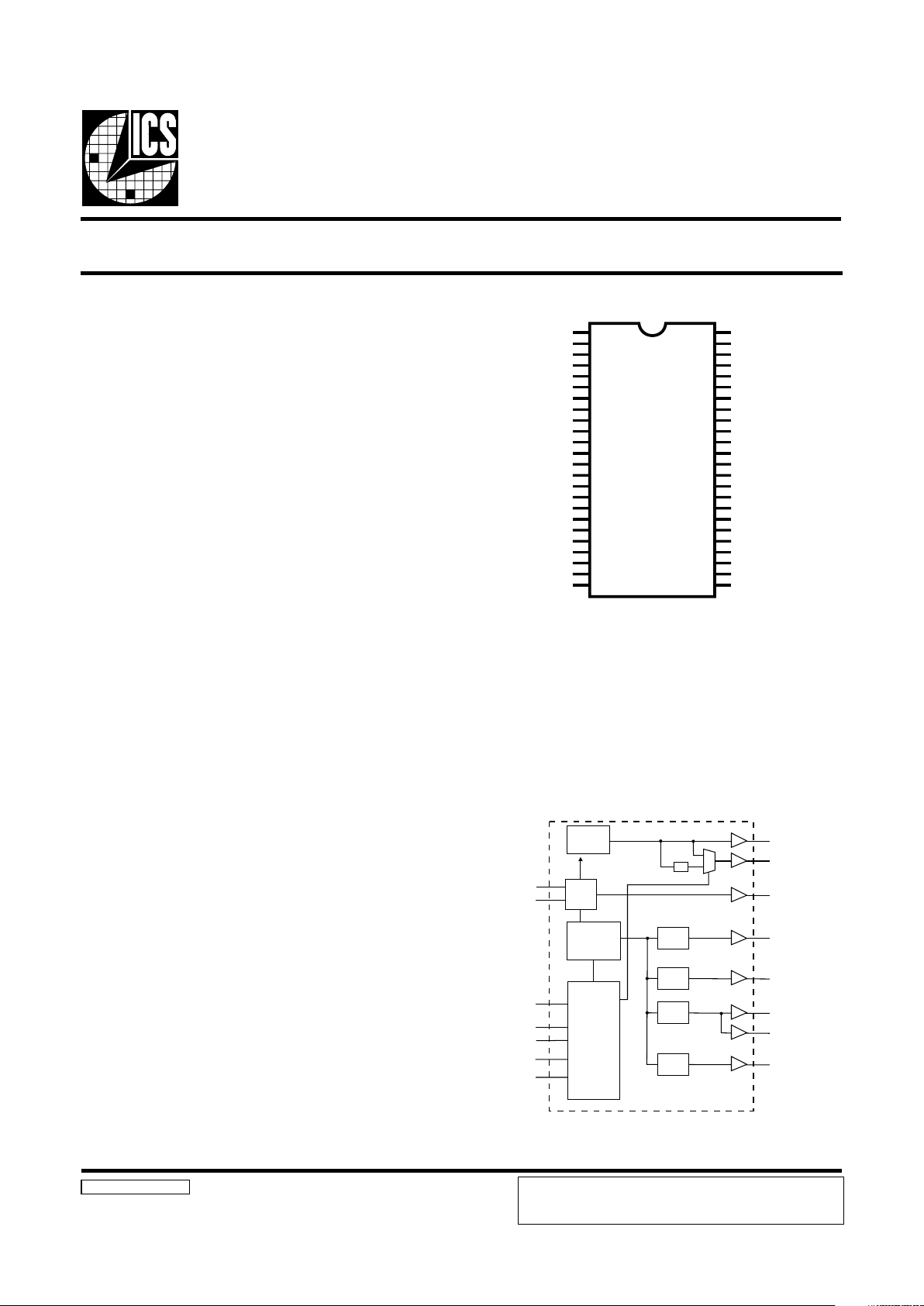
Pin Configuration
48-pin SSOP
*120K ohm pull-up to VDD on indicated inputs.
Recommended Application:
RCC chipset
Output Features:
• 4 - CPUs @ 2.5V , up to 180MHz.
• 3 - IOAPIC @ 2.5V
• 3 - 3V66MHz @ 3.3V .
• 11 - PCIs @ 3.3V
• 1 - 48MHz, @ 3.3V fixed
• 1 - 24/48MHz, @ 3.3V
Features:
• Up to 180MHz frequency support
• Use a zero delay buffer such as the ICS9179-06 to
generate SDRAM clocks.
• Support power management: Power down Mode
from I2C programming.
• Spread spectrum for EMI control
± 0.25% center spread).
• Uses external 14.318MHz crystal
• 5 - FS pins for frequency select
Key Specifications:
• CPU Output Jitter: <250ps
• IOAPIC Output Jitter: <500ps
• 48MHz, 3V66, PCI Output Jitter: <500ps
• Ref Output Jitter. <1000ps
• CPU Output Skew: <175ps
• IOAPIC Output Skew <250ps
• PCI Output Skew: <580ps
• 3V66 Output Skew <250ps
• CPU to 3V66 Output Offset: 0.8 - 1.8ns (typ = 1.3ns)
• CPU to PCI Output Offset: 0.0 - 1.5ns (typ = 1.0ns)
• CPU to IOAPIC Output Offset: 1.5 - 4.0ns (typ = 2.0ns)
SEL24_48#
PLL2
PLL1
Spread
Spectrum
48MHz
24_48MHz
CPUCLK (3:0)
IOAPIC (2:0)
PCICLK (10:0)
PCICLK_F
3V66 (2:0)
X1
X2
XTAL
OSC
CPU
DIVDER
IOAPIC
DIVDER
PCI
DIVDER
3V66
DIVDER
S DATA
SCLK
IC
2
FS(4:0)
PD#
Control
Logic
Config.
Reg.
/ 2
REF(1:0)
{
GNDREF
REF0
*SEL24_48#/REF1
VDDREF
X1
X2
GNDPCI
*FS0/PCICLK_F
*FS1/PCICLK1
VDDPCI
*FS2/PCICLK2
*FS3/PCICLK3
GNDPCI
PCICLK4
PCICLK5
VDDPCI
PCICLK6
PCICLK7
GNDPCI
PCICLK8
PCICLK9
PCICLK10
VDDPCI
PD#
ICS9248-107
1
2
3
4
5
6
7
8
9
10
11
12
13
14
15
16
17
18
19
20
21
22
23
24
48
47
46
45
44
43
42
41
40
39
38
37
36
35
34
33
32
31
30
29
28
27
26
25
VDDLAPIC
IOAPIC0
IOAPIC1
GNDLAPIC
IOAPIC2
VDDLCPU
CPUCLK0
GNDLCPU
CPUCLK1
VDDLCPU
CPUCLK2
CPUCLK3
GNDLCPU
VDD66
3V66_0
3V66_1
3V66_2
GND66
S DATA
SCLK
VDD48
48MHz/FS4*
24_48MHz
GND48
{
I
C
2
ICS reserves the right to make changes in the device data identified in
this publication without further notice. ICS advises its customers to
obtain the latest version of all device data to verify that any
information being relied upon by the customer is current and accurate.
Page 2
2
ICS9248-107
Pin Descriptions
The ICS9248-107 is a main clock synthesizer chip for Pentium II based systems using Rambus Interface DRAMs. This chip
provides all the clocks required for such a system when used with a zero delay buffer such as the ICS9179-06.
Spread Spectrum may be enabled through I2C. Spread spectrum typically reduces system EMI by 8dB to 10dB. This simplifies
EMI qualification without resorting to board design iterations or costly shielding. The ICS9248-107 employs a proprietary
closed loop design, which tightly controls the percentage of spreading over process and temperature variations.
General Description
Pin number Pin name Type Description
1, 7, 13, 19, 25, 31 GND PWR Ground pins
2 REF0 OUT 14.318MHz reference clock outputs at 3.3V
REF1 OUT 14.318MHz reference clock outputs at 3.3V
SEL24_48# IN Logic input to select 24 or 48MHz for pin 26 output
4, 10, 16, 23,
28, 35
VDD PWR Power pins 3.3V
5 X1 IN X TAL_IN 14.318M Hz crystal input
6 X 2 OU T XTAL_OUT Crystal output
PCICLK_F OUT Free running PCI clock at 3.3V. Synchronous to CPU clocks.
FS 0 IN Logic - input for frequency selection
PCICLK1 OUT PCI clock output at 3.3V. Synchronous to CPU clocks.
FS 1 IN Logic - input for frequency selection
PCICLK2 OUT PCI clock output at 3.3V. Synchronous to CPU clocks.
FS 2 IN Logic - input for frequency selection
PCICLK3 OUT PCI clock output at 3.3V. Synchronous to CPU clocks.
FS 3 IN Logic - input for frequency selection
14, 15, 17, 18, 20,
21, 22
PCICLK (4:10) OUT PCI clock outputs at 3.3V. Synchronous to CPU clocks.
24 PD# IN
This asynchronous input powers down the chip when drive
active(Low). The internal PLLs are dis abled and all the output clocks
are held at a Low s tate.
26 24_48MHz OUT
24 or 48MHz output selectable by
SEL24_48# (0=48MHz 1=24MHz)
48MHz OUT Fixed 48MHz clock output at 3.3V
FS 4 IN Logic - input for frequency selection
29 SCLK IN
Clock in
p
ut of I2C input
30 SDATA I/O Data pin for I2C circuitry 5V tolerant
32, 33, 34 3V66(2:0) OUT 3.3V clock outputs.
36, 41 GNDLCPU PWR Ground pins for CPUCLKs
37, 38, 40, 42 CPUCLK(3:0) OUT Host bus clock output at 2.5V.
39, 43 VDDLCPU PWR Power pins for CPUCLKs. 2.5V
45 GNDLAPIC PWR Ground pin for the IOAPIC outputs.
44, 46, 47 IOAPIC(2:0) OUT IOAPIC clocks at 2.5V. Synchronous with CPUCLKs.
48 VDDLAPIC PWR Power pin for the IOAPIC outputs. 2.5V.
27
12
3
8
9
11
Page 3
3
ICS9248-107
Functionality
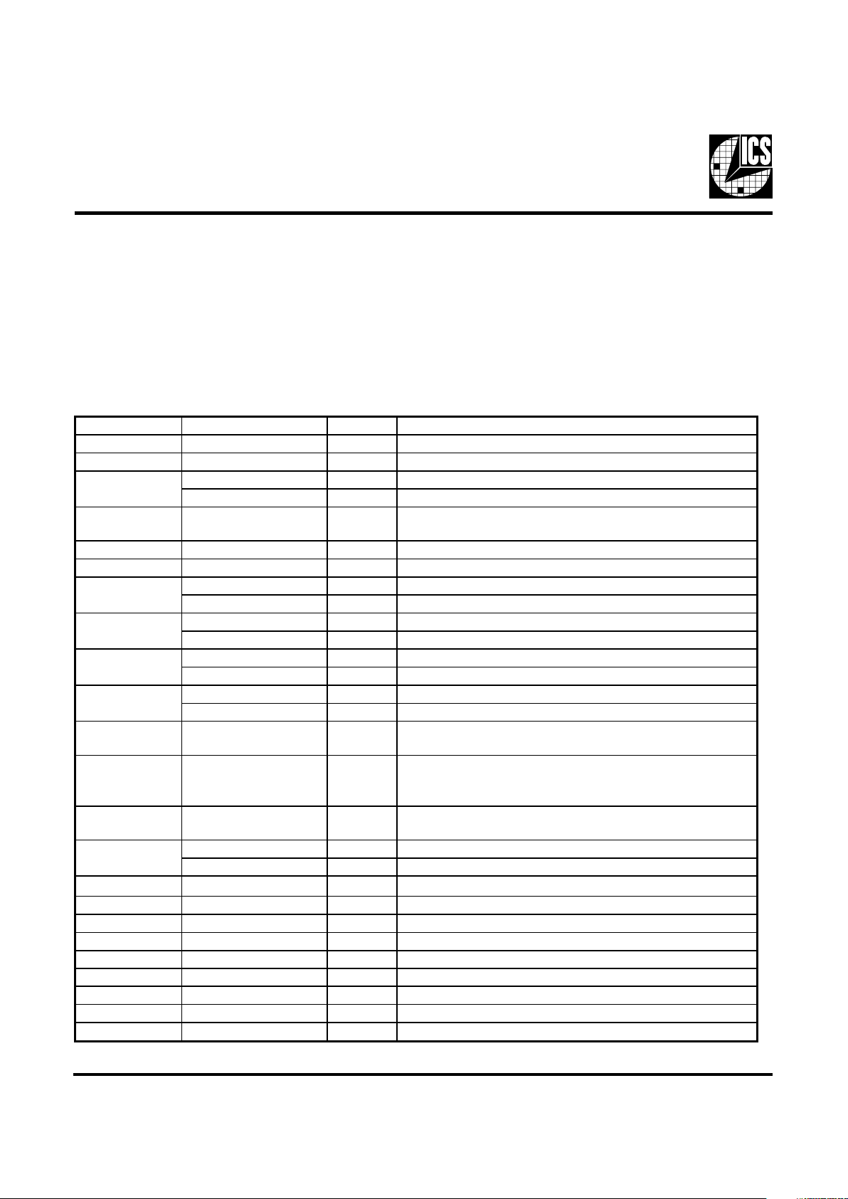
FS4 FS3 FS2 FS1 FS0 CPU PCI 3V66 IOAPI C
0 0 0 0 0 103.0 34.33 68.67 17.17
0 0 0 0 1 100.0 33.33 66.67 16.67
0 0 0 1 0 100.5 33.48 66.97 16.74
0 0 0 1 1 100.9 33.63 67.27 16.82
0 0 1 0 0 107.1 35.70 71.40 17.85
0 0 1 0 1 109.0 36.33 72.67 18.17
0 0 1 1 0 112.0 37.33 74.67 18.67
0 0 1 1 1 114.0 28.50 57.00 14.25
0 1 0 0 0 116.0 29.00 58.00 14.50
0 1 0 0 1 118.0 29.50 59.00 14.75
0 1 0 1 0 133.3 33.33 66.65 16.66
0 1 0 1 1 120.0 30.00 60.00 15.00
0 1 1 0 0 122.0 30.50 61.00 15.25
0 1 1 0 1 125.0 31.25 62.50 15.63
0 1 1 1 0 50.0 16.67 33.33 8.33
0 1 1 1 1 66.7 16.67 33.33 8.33
1 0 0 0 0 133.3 33.33 66.67 16.67
1 0 0 0 1 133.9 33.48 66.95 16.74
1 0 0 1 0 138 34.5 69 17.25
1 0 0 1 1 142 35.5 71 17.75
1 0 1 0 0 146 36.5 73 18.25
1 0 1 0 1 150 37.5 75 18.75
1 0 1 1 0 153 38.25 76.5 19.13
1 0 1 1 1 156 39 78 19.5
1 1 0 0 0 159.1 39.78 79.55 19.89
1 1 0 0 1 162 40.5 81 20.25
1 1 0 1 0 166.7 41.67 83.33 20.83
1 1 0 1 1 168 42 84 21
1 1 1 0 0 171 42.75 85.5 21.38
1 1 1 0 1 174 43.5 87 21.75
1 1 1 1 0 177 44.25 88.5 22.13
1 1 1 1 1 180 45 90 22.5
Page 4
4
ICS9248-107
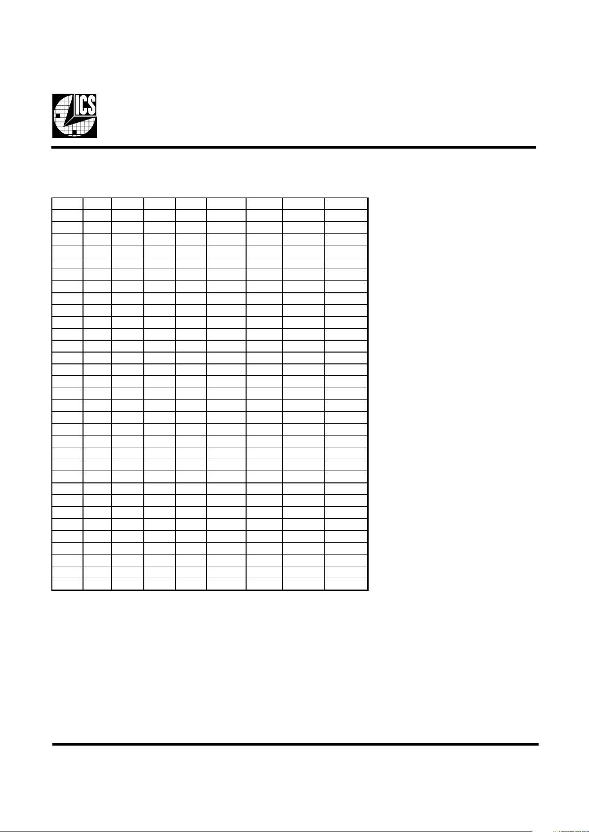
Byte 0: Functionality and frequency select register (Default = 0)
Serial Configuration Command Bitmap
Note 1:
Default at power-up will be for latched logic inputs to define frequency , as displayed byBit 3.
tiBnoitpircseDDWP
tiB
)4:7,2(
2tiB
4SF
7tiB
3SF
6tiB
2SF
5tiB
1SF
4tiB
0SF
UPCICP66V3CIPAOI
01000
1etoN
00000 0.30133.4376.8671.71
00001 0.00133.3376.6676.61
00010 54.00184.3379.6647.61
00011 9.00136.3372.7628.61
00100 1.70107.5304.1758.71
00101 0.90133.6376.2771.81
00110 0.21133.7376.4776.81
00111 00.41105.8200.7552.41
01000 00.61100.9200.8505.41
01001 00.81105.9200.9557.41
01010 03.33133.3356.6666.61
01011 00.02100.0300.0600.51
01100 00.22105.0300.1652.51
01101 00.52152.1305.2636.51
01110 0.0576.6133.3333.8
01111 7.6676.6133.3333.8
10000 3.33133.3376.6676.61
10001 9.33184.3359.6647.61
10010 0.83105.4300.9652.71
10011 0.24105.5300.1757.71
10100 0.64105.6300.3752.81
10101 0.05105.7300.5757.81
10110 0.35152.8305.6731.91
10111 0.65100.9300.8705.91
11000 1.95187.9355.9798.91
11001 0.26105.0400.1852.02
11010 7.66176.1433.3838.02
11011 0.86100.2400.4800.12
11100 0.17157.2405.5883.12
11101 0.47105.3400.7857.12
11110 0.77152.4405.8831.22
11111 0.08100.5400.0905.22
3tiB
stupnidehctal,tceleserawdrahybdetcelessiycneuqerF-0
4:7,2tiBybdetcelessiycneuqerF-1
0
1tiB
lamroN-0
delbanemurtcepsdaerpS-1
1
0tiB
gninnuR-0
stuptuollaetatsirT-1
0
Page 5
5
ICS9248-107
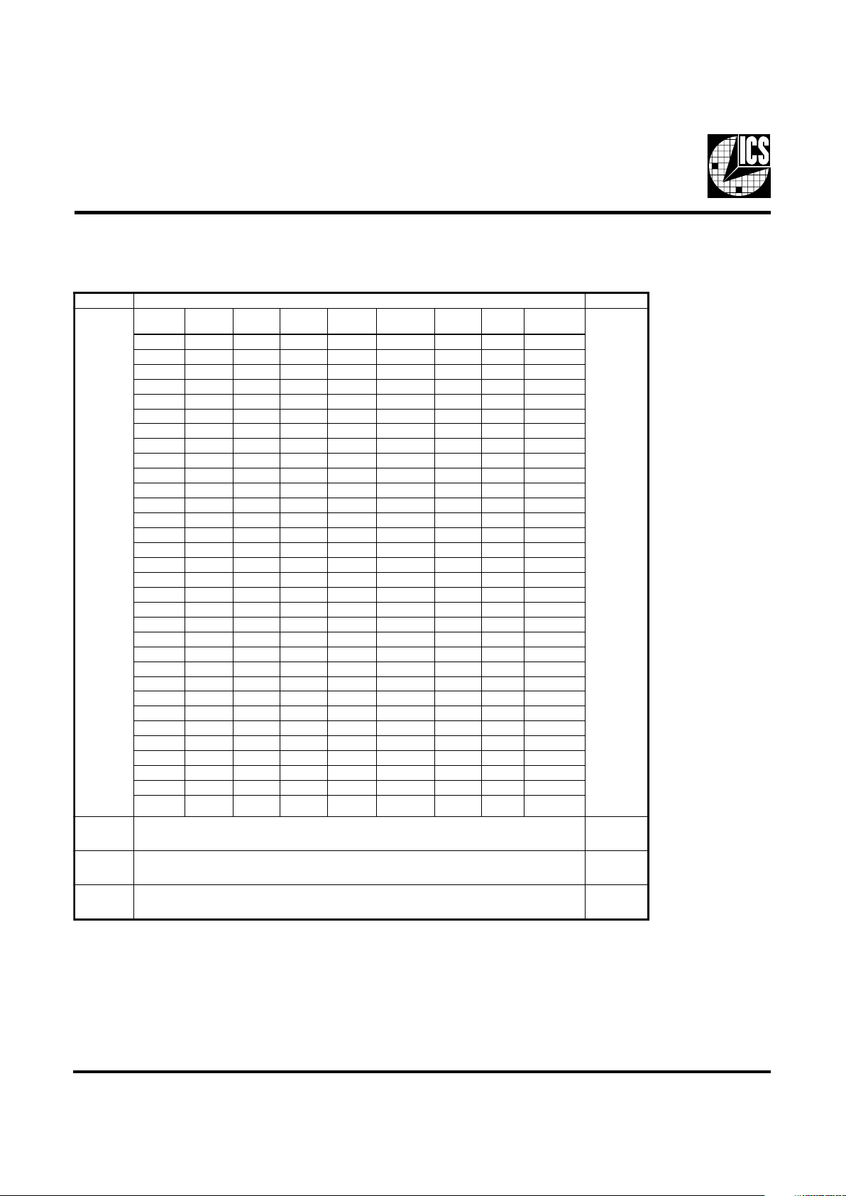
Byte 1: CPU, Active/Inactive Register
(1 = enable, 0 = disable)
Byte 2: PCI Active/Inactive Register
(1 = enable, 0 = disable)
Byte 3: 3V66 Active/Inactive Register
(1 = enable, 0 = disable)
Notes:
1. Inactive means outputs are held LOW and are disabled
from switching.
Notes:
1. Inactive means outputs are held LOW and are disabled
from switching.
Notes:
1. Inactive means outputs are held LOW and are disabled
from switching.
Byte 4: PCI Active/Inactive Register
(1 = enable, 0 = disable)
Notes:
1. Inactive means outputs are held LOW and are disabled
from switching.
tiB#niPDWPnoitpircseD
7tiB041 1KLCUPC
6tiB831 2KLCUPC
5tiB731 3KLCUPC
4tiB241 0KLCUPC
3tiB741 0CIPAOI
2tiB641 1CIPAOI
1tiB441 2CIPAOI
0tiB-X )devreseR(
tiB#niPDWPnoitpircseD
7tiB811 7KLCICP
6tiB711 6KLCICP
5tiB511 5KLCICP
4tiB411 4KLCICP
3tiB211 3KLCICP
2tiB111 2KLCICP
1tiB91 1KLCICP
0tiB81 F_KLCICP
tiB#niPDWPnoitpircseD
7tiB431 0_66V3
6tiB331 1_66V3
5tiB231 2_66V3
4tiB-X#1SF
3tiB210FER
2tiB311FER
1tiB-X#3SF
0tiB-X#2SF
tiB#niPDWPnoitpircseD
7tiB621 zHM84_42
6tiB721 zHM84
5tiB-X#0SF
4tiB-1 )devreseR(
3tiB221 01KLCICP
2tiB121 9KLCICP
1tiB021 8KLCICP
0tiB-X#4SF
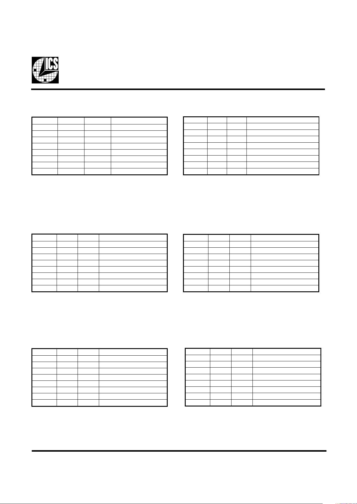
Byte 5: Active/Inactive Register
(1= enable, 0 = disable)
tiB#niPDWPnoitpircseD
7tiB-0 )etoN(devreseR
6tiB-0 )etoN(devreseR
5tiB-0 )etoN(devreseR
4tiB-0 )etoN(devreseR
3tiB-0 )etoN(devreseR
2tiB-1 )etoN(devreseR
1tiB-1 )etoN(devreseR
0tiB-0 )etoN(devreseR
Byte6: Active/Inactive Register
(1= enable, 0 = disable)
Note: Don’t write into this register, writing into this register
can cause malfunction
tiB#niPDWPnoitpircseD
7tiB-1 )etoN(devreseR
6tiB-1 )etoN(devreseR
5tiB-1 )etoN(devreseR
4tiB-1 )etoN(devreseR
3tiB-1 )etoN(devreseR
2tiB-1 )etoN(devreseR
1tiB-1 )etoN(devreseR
0tiB-1 )etoN(devreseR
Notes:
1. Inactive means outputs are held LOW and are disabled
from switching.
Page 6

6
ICS9248-107
Absolute Maximum Ratings
Supply Voltage . . . . . . . . . . . . . . . . . . . . . . . . . . . 5.5 V
Logic Inputs . . . . . . . . . . . . . . . . . . . . . . . . . . . . GND –0.5 V to VDD +0.5 V
Ambient Operating Temperature . . . . . . . . . . . . 0°C to +70°C
Storage Temperature . . . . . . . . . . . . . . . . . . . . . . –65°C to +150°C
Case Temperature . . . . . . . . . . . . . . . . . . . . . . . . 115°C
Stresses above those listed under Absolute Maximum Ratings may cause permanent damage to the device. These ratings are
stress specifications only and functional operation of the device at these or any other conditions above those listed in the
operational sections of the specifications is not implied. Exposure to absolute maximum rating conditions for extended periods
may affect product reliability .
Electrical Char ac ter istics - Input/Supply/Common Output Para me te rs
TA = 0 - 70C; VDD = V
DDL
= 3.3 V +/-5% (unless otherwise stated)
PARAMETER SYMBOL CONDITIONS MIN TYP MAX UNITS
Input High Voltage V
IH
2V
DD
+0.3 V
Input Low Voltage V
IL
VSS-0.3 0.8 V
Input High Current I
IH
VIN = V
DD
5
µA
Input Low Current I
IL1
VIN = 0V; Inputs with no pull-up resistors -5
µ
A
Input Low Current I
IL2
VIN = 0V; Inputs with pull-up resistors -200
µ
A
I
DD3.3OP100
CL = 0 pF; Select @ 100 MHz 160 mA
I
DD3.3OP133
CL = 0 pF; Select @ 133 MHz 160 mA
Powerdown Current
I
DD3.3PD
CL = 0 pF; PWRDWN#=0
600
µ
A
Input Frequency F
i
VDD = 3.3 V 11 14.318 16 MHz
C
IN
Logic Inputs 5 pF
C
INX
X1 & X2 pins 27 45 pF
Transition time
1
T
trans
To 1st crossing of target frequency 3 ms
Settling Time
1
T
s
From 1st crossing to 1 % target frequency. 3 ms
Clk Stabilization
1
T
STAB
From VDD = 3.3 V to 1% target frequency
3ms
1
Guaranteed by design, not 100% tested in production.
Input Capacitance
1
Operating Supply
Current
Electrical Characteristics - Input/ Supply/Common Output Parameters
TA = 0 - 70C; VDD = 3.3 V +/- 5%, V
DDL
= 2.5V +/- 5% (unless otherwise stated).
PARAMETER SYMBOL CONDITIONS MIN TYP MAX UNITS
I
DD2.5OP100
CL = 0 pF; Select @ 100 MHz 75 mA
I
DD2.5OP133
CL = 0 pF; Select @ 133 MHz 90 mA
Power Down Supply Current
I
DD2.5PD
CL = 0 pF; PWRDWN# = 0
100
µA
Operating Supply Current
Page 7

7
ICS9248-107
Electrical Characteristics - Group Offset
TA = 0 - 70C; VDD = 3.3 V +/- 5%, V
DDL
= 2.5V +/- 5% (unless other wise stated).
Group Offset Measurement Loads Measurement Points
CPU to 3V66 0.8 to 1.8 ns C PU leads
CPU @ 20 pF, 3V66 @ 30 pF CPU @ 1.25V, 3V66 @ 1.5 V
CPU to PCI 0 to 1.5 ns CPU leads
CPU @ 20 pF, PCI @ 30 pF CPU @ 1.25V, PCI @ 1.5 V
CPU to IOAPIC
1.5 to 4.0 ns CPU leads
CPU @ 20 pF, IOAPIC @ 20 pF CPU @ 1.25V, IOAPIC @ 1.25 V
Electrical Characteristics - CPUCLK
TA = 0 - 70º C; VDD = 3.3 V +/-5%, V
DDL
= 2.5V +/- 5 %; CL = 20 pF (unless otherwise stated).
PARAMETER SYMBOL CONDITIONS MIN TYP MAX UNITS
Output High Voltage V
OH2B
IOH = -12 mA 2 2.3 V
Output Low Voltage V
OL2B
IOL = 12 mA 0.3 0.4 V
Output High Current
I
OH2B
VOH = 1.7 V -35 -19
mA
Output Low Current
I
OL2B
VOL = 0.7 V 19 26
mA
Rise Time t
r2B
1
VOL = 0.4 V, VOH = 2.0 V 0.4 1.03 1.6 ns
Fall Time t
f2B
1
VOH = 2.0 V, VOL = 0.4 V 0.4 1.11 1.6 ns
d
t2B
1
VT = 1.25 V CPU frequency < 142 MHz 45 49.3 55 %
d
t2B
1
VT = 1.25 V CPU frequency > 142 MHz 42 46.4 52 %
Skew
t
sk2B
1
VT = 1.25 V 75 175 ps
Jitter, Cycle-to-cycle
t
jcyc-cyc2B
1
VT = 1.25 V
141 250 ps
1
Guaranteed by design, not 100% tested in production.
Duty Cycle
Page 8

8
ICS9248-107
Electrical Characteristics - 3V66
TA = 0 - 70º C; VDD = 3.3 V +/-5%, V
DDL
= 2.5 V +/-5%; CL = 30 pF (unless otherwise stated)
PARAMETER SYMBOL CONDITIONS MIN TYP MAX UNITS
Output High Voltage V
OH1
IOH = -25 mA 2.4 2.9 V
Output Low Voltage V
OL1
IOL = 20 mA 0.32 0.4 V
Output High Current I
OH1
VOH = 2.0 V -73 -40 mA
Output Low Current I
OL1
VOL = 0.8 V 41 50 mA
Rise Time T
r
1
VOL = 0.4 V, VOH = 2.4 V 0.5 1.41 2 ns
Fall Time T
f
1
VOH = 2.4 V, VOL = 0.4 V 0.5 1.41 2 ns
Duty Cycle D
t
1
VT = 1.5 V 45 50.1 55 %
Skew T
sk1
1
VT = 1.5 V 86 250 ps
Jitter, Cycle-to-cycle
t
jcyc-cyc1
1
VT = 1.5 V
162 500 ps
1
Guarenteed by design, not 100% tested in production.
Electrical Characteristics - PCICLK
TA = 0 - 70º C; VDD = 3.3 V +/-5%, V
DDL
= 2.5 V +/-5%; CL = 30 pF (unless otherwise stated)
PARAMETER SYMBOL CONDITIONS MIN TYP M AX UNITS
Output High Voltage V
OH1
IOH = -11 mA 2.4 3.1 V
Output Low Voltage V
OL1
IOL = 9.4 mA 0.17 0.4 V
Output High Current I
OH1
VOH = 2.0 V -62 -22 mA
Output Low Cur rent I
OL1
VOL = 0.8 V 25 45 mA
Rise Time
1
t
r1
VOL = 0.4 V, VOH = 2.4 V 0.5 1.75 2.5 ns
Fall Time
1
t
f1
VOH = 2.4 V, VOL = 0.4 V 0.5 1.58 2.5 ns
Duty Cycle
1
d
t1
VT = 1.5 V 45 50.3 55 %
t
sk1
VT = 1.5 V, PCICLK (F:7) 274 400 ps
t
sk1
VT = 1.5 V, PCICLK (8:10) 96 250 ps
t
sk1
VT = 1.5 V, PCICLK (F:10) 496 580 ps
Jitter, C
y
cle-to-cycle
1
t
jcyc-cyc1
VT = 1.5 V
133 500 ps
1
Guaranteed by design, not 100% tested in production.
Skew
1
Page 9

9
ICS9248-107
Electrical Characteristi cs - 24MHz, 48MHz
TA = 0 - 70º C; VDD = 3.3 V +/- 5%, V
DDL
= 2.5 V +/- 5 %; CL = 20 pF (unless otherwise stated).
PARAMETER SYMBOL CONDITIONS MIN TYP MAX UNITS
Output High Voltage V
OH5
IOH = -12 mA 2.6 2.9 V
Output Low Voltage V
OL5
IOL = 9 mA 0.3 0.4 V
Output High Current
I
OH5
VOH = 2.0 V -27 -22
mA
Output Low Current
I
OL5
VOL = 0.8 V 16 22
mA
Rise Time t
r5
1
VOL = 0.4 V, VOH = 2.4 V 2.05 4 ns
Fall Time t
f5
1
VOH = 2.4V, VOL = 0.4 V 2.13 4 ns
Duty Cycle d
t5
1
VT = 1.5 V 45 50.7 55 %
Jitter, Cycle-to-Cycle
t
jcyc-cyc 5
1
VT = 1.5 V
314 500 ps
1
Guaranteed by design, not 100% tested in production.
Electrical Characteristics - REF
TA = 0 - 70º C; VDD = 3.3 V +/- 5%, V
DDL
= 2.5 V +/- 5 %; CL = 20 pF (unless otherwise stated).
PARAMETER SYMBOL CONDITIONS MIN TYP MAX UNITS
Output High Voltage V
OH5
IOH = -12 mA 2.6 2.9 V
Output Low Voltage V
OL5
IOL = 9 mA 0.3 0.4 V
Output High Current
I
OH5
VOH = 2.0 V -27 -22
mA
Output Low Current
I
OL5
VOL = 0.8 V 16 22
mA
Rise Time t
r5
1
VOL = 0.4 V, VOH = 2.4 V 1.97 4 ns
Fall Time t
f5
1
VOH = 2.4V, VOL = 0.4 V 2.10 4 ns
Duty Cycle d
t5
1
VT = 1.5 V 45 52.5 55 %
Jitter, Cycle-to-Cycle
t
jcyc-cyc 5
1
VT = 1.5 V
590 1000 ps
1
Guaranteed by design, not 100% tested in production.
Page 10

10
ICS9248-107
Electrical Characteristi cs - IO APIC
TA = 0 - 70º C; VDD = 3.3 V +/-5%, V
DDL
= 2.5 V +/-5%; CL = 20 pF (unless otherwise stated)
PARAMETER SYMBOL CONDITIONS MIN TYP MAX UNITS
Output High Voltage V
OH4B
IOH = -12.0 mA 2 2.3 V
Output Low Voltage V
OL4B
IOL = 12 mA 0.31 0.4 V
Output High Current I
OH4B
VOH = 1.7 V -33 -19 mA
Output Low Current I
OL4B
VOL = 0.7 V 19 27 mA
Rise Time t
r4B
1
VOL = 0.4 V, VOH = 2.0 V 0.5 1.65 2 ns
Fall Time t
f4B
1
VOH = 2.0 V, VOL = 0.4 V 0.5 1.66 2 ns
Duty Cycle d
t4B
1
VT = 1.25 V 45 49.4 55 %
Skew
tsk4B
1
VT = 1.25 V 95 250
Jitter, Cycle-to-cycle
t
jcyc-cyc4B
1
VT = 1.25 V
120 500 ps
1
Guaranteed by design, not 100% tested in production.
Page 11

11
ICS9248-107
Power Management Features:
Note:
1. LOW means outputs held static LOW as per latency requirement next page.
2. On means active.
3. PD# pulled Low, impacts all outputs including REF and 48 MHz outputs.
Power Management Requirements:
Note:
1. Clock on/off latency is defined in the number of rising edges of free running PCICLKs between the clock disable goes low/
high to the first valid clock comes out of the device.
2. Power up latency is when PWR_DWN# goes inactive (high) to when the first valid clocks are dirven from the device.
langiSetatSlangiS
ycnetaL
fosegdegnisirfo.oN
KLCICP
#DP
)noitarepolamron(1Sm3
)nwodrewop(0.xam2
#DPKLCUPCCIPAOI66V3ICPF_ICP
.FER
zHM84
csOsOCV
0WOLWOLWOLWOLWOLWOLFFOFFO
1NONONONONONONONO
Page 12

12
ICS9248-107
1 . The ICS clock generator is a slave/receiver , I2C component. It can read back the data stored in the latches for verification.
Read-Back will support Intel PIIX4 "Block-Read" protocol.
2. The data transfer rate supported by this clock generator is 100K bits/sec or less (standard mode)
3 . The input is operating at 3.3V logic levels.
4. The data byte format is 8 bit bytes.
5. To simplify the clock generator I2C interface, the protocol is set to use only "Block-Writes" from the controller. The
bytes must be accessed in sequential order from lowest to highest byte with the ability to stop after any complete byte
has been transferred. The Command code and Byte count shown above must be sent, but the data is ignored for those
two bytes. The data is loaded until a Stop sequence is issued.
6. At power-on, all registers are set to a default condition, as shown.
General I2C serial interface information
The information in this section assumes familiarity with I2C programming.
For more information, contact ICS for an I2C programming application note.
How to Write:
• Controller (host) sends a start bit.
• Controller (host) sends the write address D2
(H)
• ICS clock will acknowledge
• Controller (host) sends a dummy command code
• ICS clock will acknowledge
• Controller (host) sends a dummy byte count
• ICS clock will acknowledge
• Controller (host) starts sending first byte (Byte 0)
through byte 6
• ICS clock will acknowledge each byte one at a time.
• Controller (host) sends a Stop bit
How to Read:
• Controller (host) will send start bit.
• Controller (host) sends the read address D3
(H)
• ICS clock will acknowledge
• ICS clock will send the byte count
• Controller (host) acknowledges
• ICS clock sends first byte (Byte 0) through byte 6
• Controller (host) will need to acknowledge each byte
• Controller (host) will send a stop bit
Notes:
Controller (Host) ICS (Slave/Receiver)
Start Bit
Address
D2
(H)
A
CK
Dummy Command Code
A
CK
Dummy Byte Count
A
CK
Byte 0
ACK
Byte 1
A
CK
Byte 2
A
CK
Byte 3
ACK
Byte 4
A
CK
Byte 5
A
CK
Byte 6
ACK
Stop Bit
How to Wri te:
Controller (Host) ICS (Slave/Receiver)
Start Bit
Address
D3
(H)
A
CK
Byte Count
ACK
Byte 0
ACK
Byte 1
ACK
Byte 2
ACK
Byte 3
ACK
Byte 4
ACK
Byte 5
ACK
Byte 6
ACK
Stop Bit
How to Read:
Page 13

13
ICS9248-107
PD# Timing Diagram
The power down selection is used to put the part into a very low power state without turning off the power to the part. PD# is
an asynchronous active low input. This signal needs to be synchronized internal to the device prior to powering down the clock
synthesizer.
Internal clocks are not running after the device is put in power down. When PD# is active low all clocks need to be driven to a
low value and held prior to turning off the VCOs and crystal. The power up latency needs to be less than 3 mS. The power down
latency should be as short as possible but conforming to the sequence requirements shown below . The REF and 48MHz clocks
are expected to be stopped in the LOW state as soon as possible. Due to the state of the internal logic, stopping and holding
the REF clock outputs in the LOW state may require more than one clock cycle to complete.
Notes:
1. All timing is referenced to the Internal CPUCLK (defined as inside the ICS9248 device).
2. As shown, the outputs Stop Low on the next falling edge after PD# goes low.
3. PD# is an asynchronous input and metastable conditions may exist. This signal is synchronized inside this part.
4. The shaded sections on the VCO and the Crystal signals indicate an active clock.
5. Diagrams shown with respect to 133MHz. Similar operation when CPU is 100MHz.
CPUCLK
3V66
PCICLK
VCO
Crystal
PD#
Page 14

14
ICS9248-107
Ordering Information
ICS9248yF-107
Pattern Number (2 or 3 digit number for parts with ROM code patterns)
Package Type
F=SSOP
Revision Designator
Device Type
Prefix
ICS, AV = Standard Device
Example:
ICS XXXX y F - PPP
ICS reserves the right to make changes in the device data identified in
this publication without further notice. ICS advises its customers to
obtain the latest version of all device data to verify that any
information being relied upon by the customer is current and accurate.
INDEX
AREA
INDEX
AREA
12
1 2
N
D
h x 45°
h x 45°
E1
E
SEATING
PLANE
SEATING
PLANE
A1
A
e
-C-
- C -
b
.10 (.004) C
.10 (.004) C
c
L
300 mil SSOP Package
MIN MAX MIN MAX
A 2.41 2.80 .095 .110
A1 0.20 0.40 .008 .016
b 0.20 0.34 .008 .0135
c 0.13 0.25 .005 .010
D
E 10.03 10.68 .395 .420
E1 7.40 7.60 .291 .299
e
h 0.38 0.64 .015 .025
L 0.50 1.02 .020 .040
N
α
0° 8° 0° 8°
MIN MAX MIN MAX
48 15.75 16.00 .620 .630
10-0034
SYMBOL
In Millimeters In Inches
COMMON DIMENSIONS COMMON DIMENSIONS
SEE VARIATIONS SEE VARIATIONS
0.635 BASIC 0.025 BASIC
Reference Doc.: JEDEC Publication 95, MO-118
VARIATIONS
SEE VARIATIONS SEE VARIATIONS
N
D mm. D (inch)
 Loading...