

Page 1
Integrated
Circuit
Systems, Inc.
General Description Features
ICS9248-55
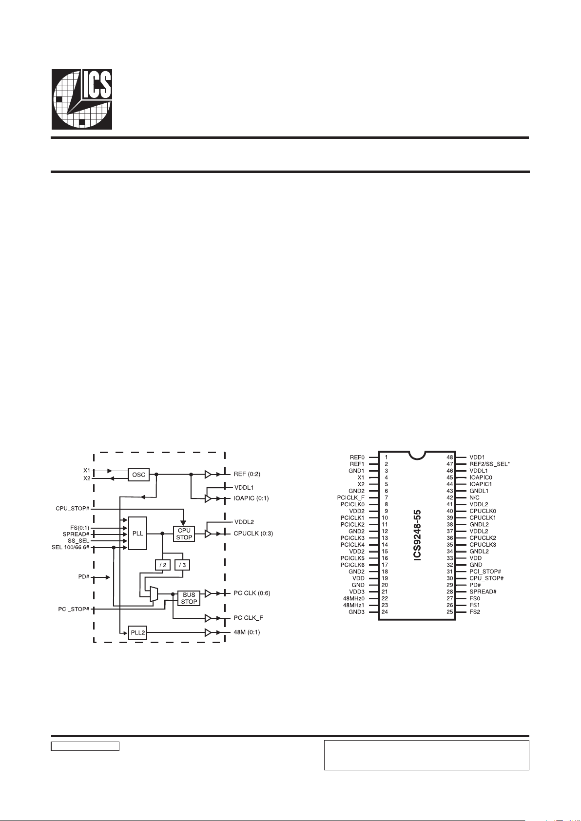
Block Diagram
Pentium/Pro/IITM System Clock Chip
9248-55 Rev B 12/04/98
Pin Configuration
48-Pin SSOP
Pentium is a trademark on Intel Corporation.
Generates system clocks for CPU, IOAPIC, PCI, plus
14.314 MHz REF (0:2), USB, and Super I/O
Supports single or dual processor systems
Supports Spread Spectrum modulation for CPU & PCI
clocks, down spread -0.5%
Skew from CPU (earlier) to PCI clock (rising edges for
100/33.3MHz) 1.5 to 4ns
Two fixed outputs at 48MHz.
Separate 2.5V and 3.3V supply pins
2.5V or 3.3V output: CPU, IOAPIC
3.3V outputs: PCI, REF, 48MHz
No power supply sequence requirements
Uses external 14.318MHz crystal, no external load cap
required for CL=18pF crystal
48 pin 300 mil SSOP
The ICS9248-55 is a Clock Synthesizer chip for Pentium and
PentiumPro CPU based Desktop/Notebook systems that will
provide all necessary clock timing.
Features include four CPU and eight PCI clocks. Three
reference outputs are available equal to the crystal frequency.
Additionally, the device meets the Pentium power-up
stabilization requirement, assuring that CPU and PCI clocks
are stable within 2ms after power-up.
PD# pin enables low power mode by stopping crystal OSC
and PLL stages. Other power management features include
CPU_STOP#, which stops CPU (0:3) clocks, and PCI_STOP#,
which stops PCICLK (0:6) clocks.
High drive CPUCLK outputs typically provide greater than 1
V/ns slew rate into 20pF loads. PCICLK outputs typically
provide better than 1V/ns slew rate into 30pF loads while
maintaining 50±5% duty cycle. The REF clock outputs typically
provide better than 0.5V/ns slew rates.
The ICS9248-55 accepts a 14.318MHz reference crystal or
clock as its input and runs on a 3.3V core supply.
Power Groups
VDD = Supply for PLL core
VDD1 = REF (0:2), X1, X2
VDD2 = PCICLK_F, PCICLK (0:6)
VDD3 = 48MHz0, 48MHz1
VDDL1 = IOAPIC (0:1)
VDDL2 = CPUCLK (0:3)
Ground Groups
GND = Ground for PLL core
GND1 = REF (0:2), X1, X2
GND2 = PCICLK_F, PCICLK (0:6)
GND3 = 48MHz0, 48MHz1
GNDL1 = IOAPIC (0:1)
GNDL2 = CPUCLK (0:3)
ICS reserves the right to make changes in the device data identified in
this publication without further notice. ICS advises its customers to
obtain the latest version of all device data to verify that any
information being relied upon by the customer is current and accurate.
* Internal Pull-down Resistor of
240K to GND. on indicated inputs
Page 2
2
ICS9248-55
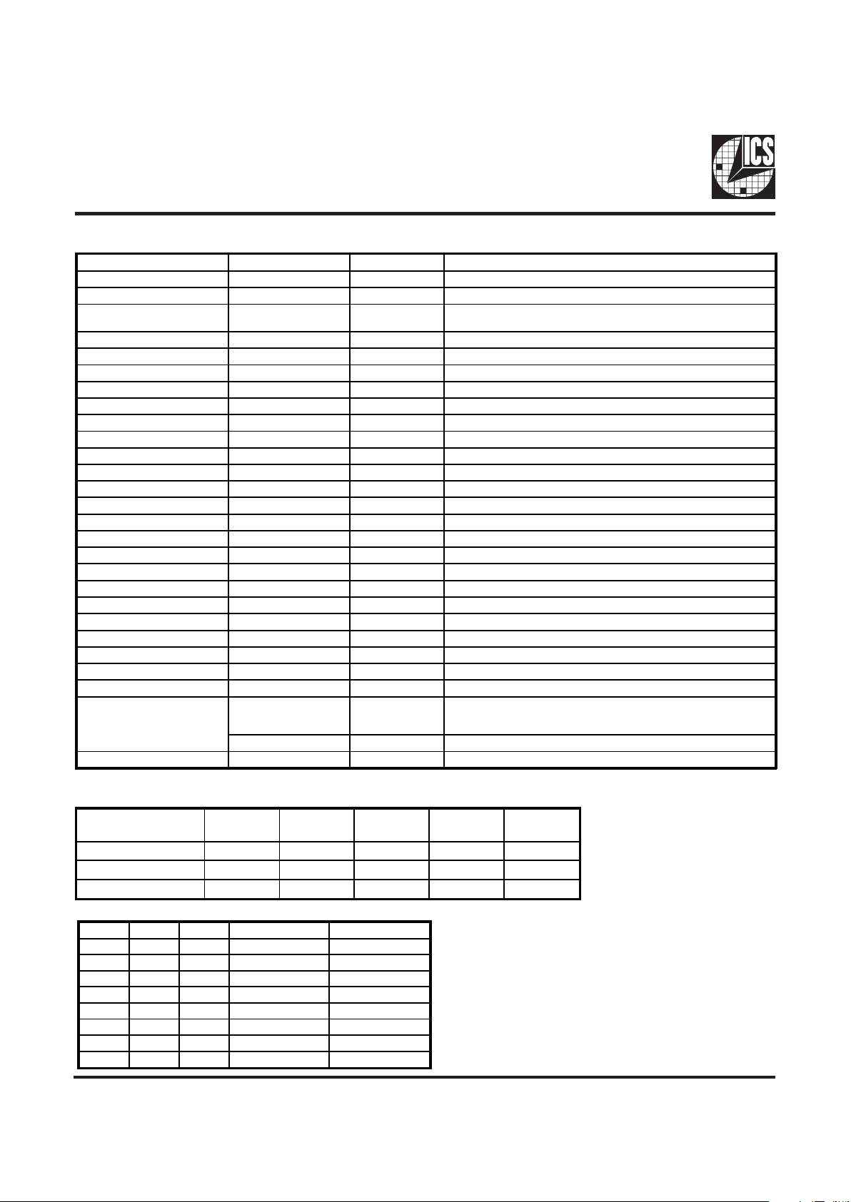
Pin Descriptions
Select Functions
Functionality CPU
PCI,
PCI_F
REF IOAPIC
48 MHz
Selection
Tristate HI - Z HI - Z HI - Z HI - Z HI - Z
Testmode T CLK/2
1
TCLK/6
1
TCLK
1
TCLK
1
TCLK/2
1
Spread Spectrum Modulated2Modulated214.318MHz 14.318MHz 48.0MHz
PIN NUMBER PIN NAME TYPE DESCRIPTION
1, 2 REF0, REF1 OUT 14.318MHz clock output
3 GND1 PWR Ground for REF outputs
4X1IN
XTAL_IN 14.318MHz Crystal input, has internal 33pF
load cap and feed back resistor from X2
5 X2 OUT XTAL_OUT Crystal ou tput, has in ternal load cap 33pF
6, 12, 18 GND2 PWR Ground for PCI outputs
7 PCICLK_F OUT Free Running PCI output
8, 10, 11, 13, 14, 16, 17 PCICLK (0:6) OUT PCI clock outputs. TTL compatible 3.3V
9, 15 VDD2 PWR Power for PCICLK outputs, nominally 3.3V
19, 33 VDD PWR Isolat ed power for c ore, nom inally 3.3V
20, 32 GND PWR Isolated ground for core
21 VDD3 PWR Power for 48MHz outputs, nominally 3.3V
22, 23 48MHz (0:1) OUT 48MHz outputs
24 GND3 P WR Ground for 48MHz outputs
25, 26, 27 FS (0:2) IN Frequency Select pins
28 SPREAD# IN Enables Spread Spectrum feature when LOW
29 PD# IN Powers down chip, active low
30 CPU_STOP# IN Halts CPU clocks at logic "0" level when low
31 PCI_STOP# I N Halts PCI Bus at logic "0" level when low
37, 41 VDDL2 PWR Power for CPU outputs, nominally 2.5V
34, 38 GNDL2 PWR Ground for CPU outputs.
35, 36, 39, 40 CPUCLK (3:0) OUT CPU and Host clock outputs @ 2.5V
42 N/C - Not internally connected
43 GNDL1 PWR Ground for IOAPIC outputs
44, 45 IOAPIC (0:1) OUT IOAPIC outputs (14.318MHz) @ 2.5V
46 VDDL1 PWR Power for IOAPIC outputs, nominally 2.5V
47
SS_SEL IN
±.25% Spread Spectrum Selector at power up.
Logic 0 for Downspread
Logic 1 for Centerspread
REF2 OUT 14.318MHz clock output
48 VDD1 PWR Supply for REF (0:2), X1, X2, nominal 3.3V
FS2 FS1 FS0 CPU MHz PCI MHz
0 0 0 133 33.25
0 0 1 83.3 41.65
010 75 37.5
0 1 1 66.6 33.3
1 0 0 124 41.33
1 0 1 133 44.3
1 1 0 112 37.3
1 1 1 100 33.3
Page 3
3
ICS9248-55
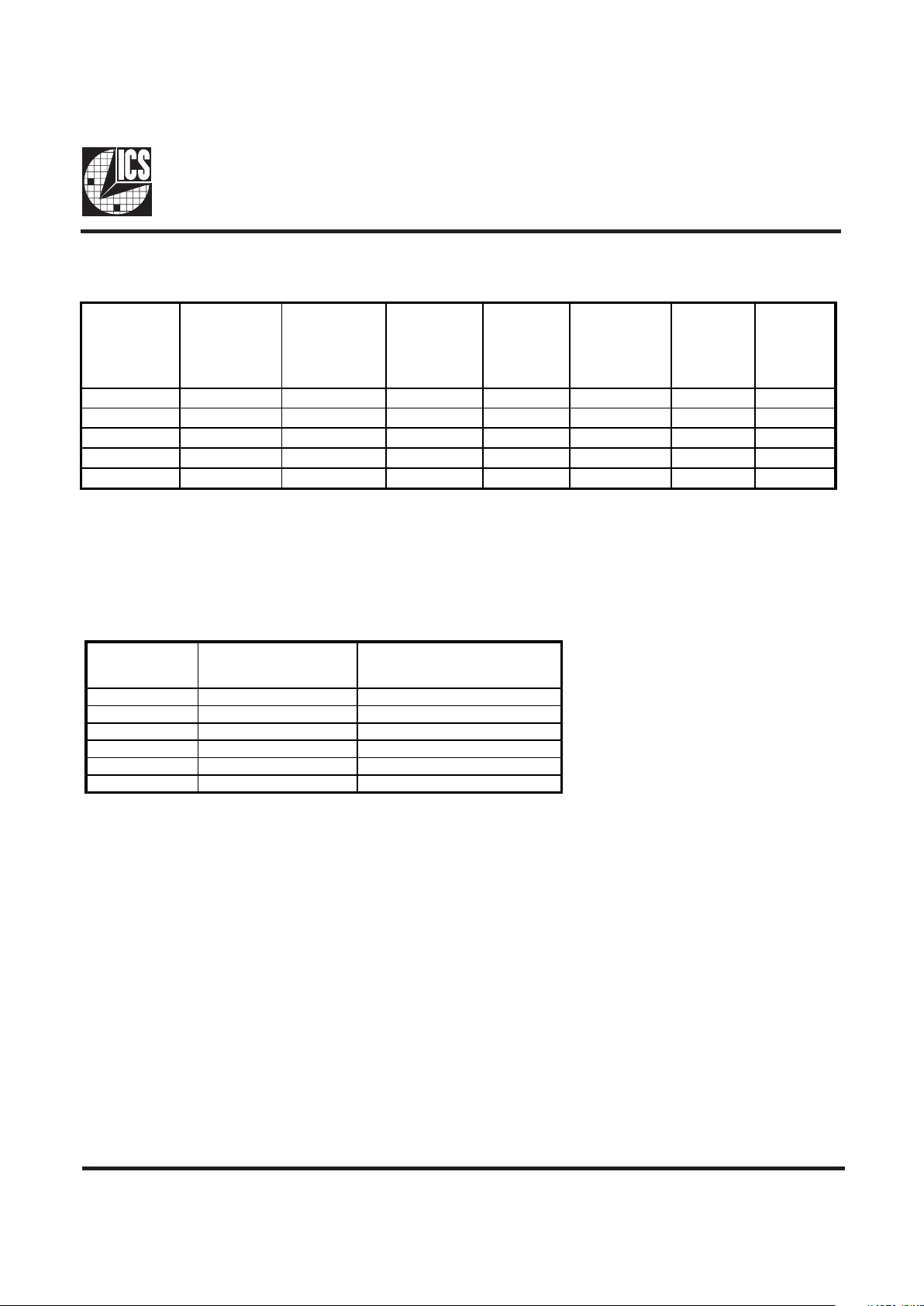
Power Management
ICS9248-55 Power Management Requirements
Clock Enable Configuration
Full clock cycle timing is guaranteed at all times after the system has initially powered up except where noted. During power
up and power down operations using the PD# select pin will not cause clocks of a shorter or longer pulse than that of the
running clock. The first clock pulse coming out of a stopped clock condition may be slightly distorted due to clock network
charging circuitry. Board routing and signal loading may have a large impact on the initial clock distortion also.
Notes.
1. Clock on latency is defined from when the clock enable goes active to when the first valid clock comes out of the device.
2. Clock off latency is defined from when the clock enable goes inactive to when the last clock is driven low out of the device.
3. Power up latency is when PD# goes inactive (high) to when the first valid clocks are output by the device.
4. Power down has controlled clock counts applicable to CPUCLK, PCICLK only.
The REF and IOAPIC will be stopped independent of these.
SIGNAL SIGNAL STATE
Latency
No. of rising edges of free
running PCICLK
CPU_ STOP# 0 (Disabled)
2
1
1 (Enabled)
1
1
PCI_STOP# 0 (Disabled)
2
1
1 (Enabled)
1
1
PD# 1 (N ormal Op eration )
3
3ms
0 (Power Down)
4
2max
CPU_STOP# PCI_STOP# PWR_DWN# CPUCLK PCICLK
Other Clocks,
REF,
IOAPICs,
48 MHz 0
48 MHz 1
Crystal VCOs
X X 0 Low Low Stopped Off Off
0 0 1 Low Low Running Running Running
0 1 1 Low Run ning Running Running Runn ing
1 0 1 Running Low Runnin g Running Running
1 1 1 Running Running Running Running Running
Page 4
4
ICS9248-55
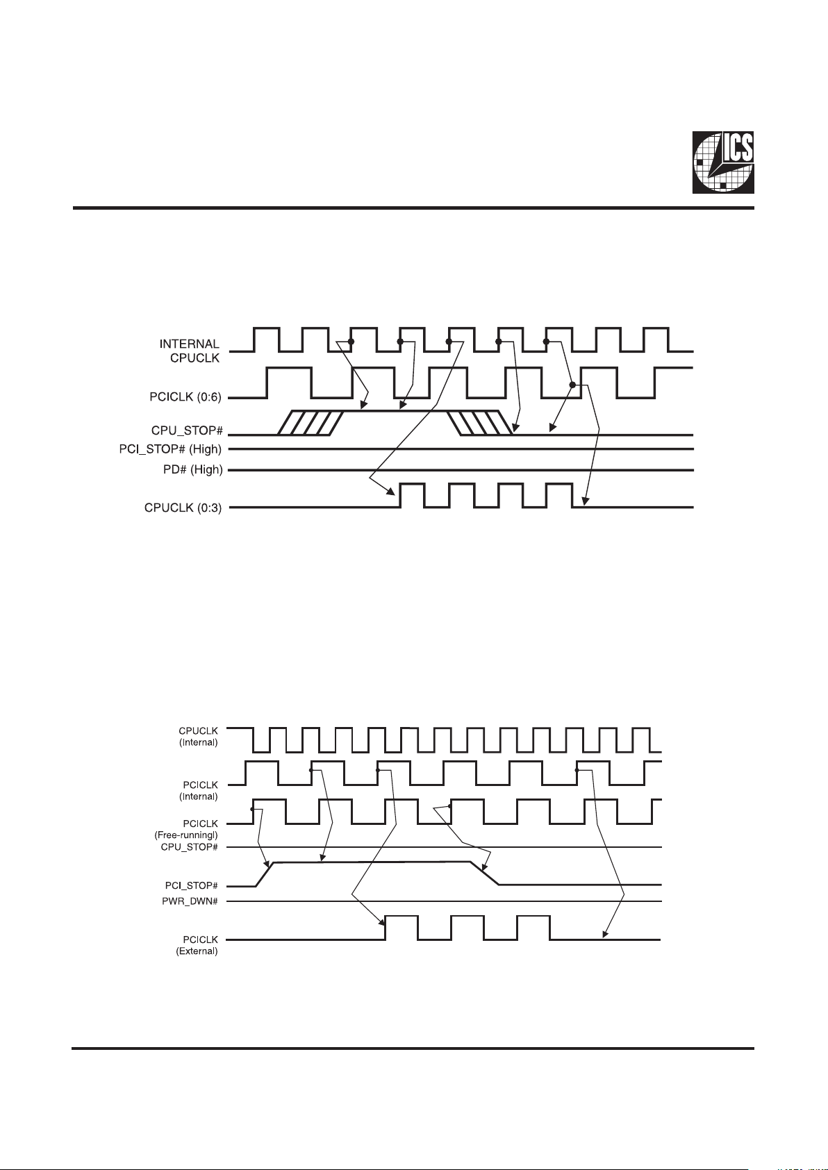
PCI_STOP# Timing Diagram
PCI_STOP# is an asynchronous input to the ICS9248-55. It is used to turn off the PCICLK (0:6) clocks for low power operation.
PCI_STOP# is synchronized by the ICS9248-55 internally. The minimum that the PCICLK (0:6) clocks are enabled (PCI_STOP#
high pulse) is at least 10 PCICLK (0:6) clocks. PCICLK (0:6) clocks are stopped in a low state and started with a full high pulse
width guaranteed. PCICLK (0:6) clock on latency cycles are only one rising PCICLK. Clock off latency is one PCICLK clock.
CPU_STOP# Timing Diagram
CPUSTOP# is an asychronous input to the clock synthesizer. It is used to turn off the CPUCLKs for low power operation.
CPU_STOP# is synchronized by the ICS9248-55. The minimum that the CPUCLK is enabled (CPU_STOP# high pulse) is 100
CPUCLKs. All other clocks will continue to run while the CPUCLKs are disabled. The CPUCLKs will always be stopped in a low
state and start in such a manner that guarantees the high pulse width is a full pulse. CPUCLK on latency is less than 4 CPUCLKs
and CPUCLK off latency is less than 4 CPUCLKs.
Notes:
1. All timing is referenced to the internal CPUCLK.
2. CPU_STOP# is an asynchronous input and metastable conditions may exist. This signal is synchronized to
the CPUCLKs inside the ICS9248-55.
3. All other clocks continue to run undisturbed.
4. PD# and PCI_STOP# are shown in a high (true) state.
Notes:
1. All timing is referenced to the Internal CPUCLK (defined as inside the ICS9248 device.)
2. PCI_STOP# is an asynchronous input, and metastable conditions may exist. This signal is required to be synchronized
inside the ICS9248-55.
3. All other clocks continue to run undisturbed.
4. PD# and CPU_STOP# are shown in a high (true) state.
Page 5
5
ICS9248-55
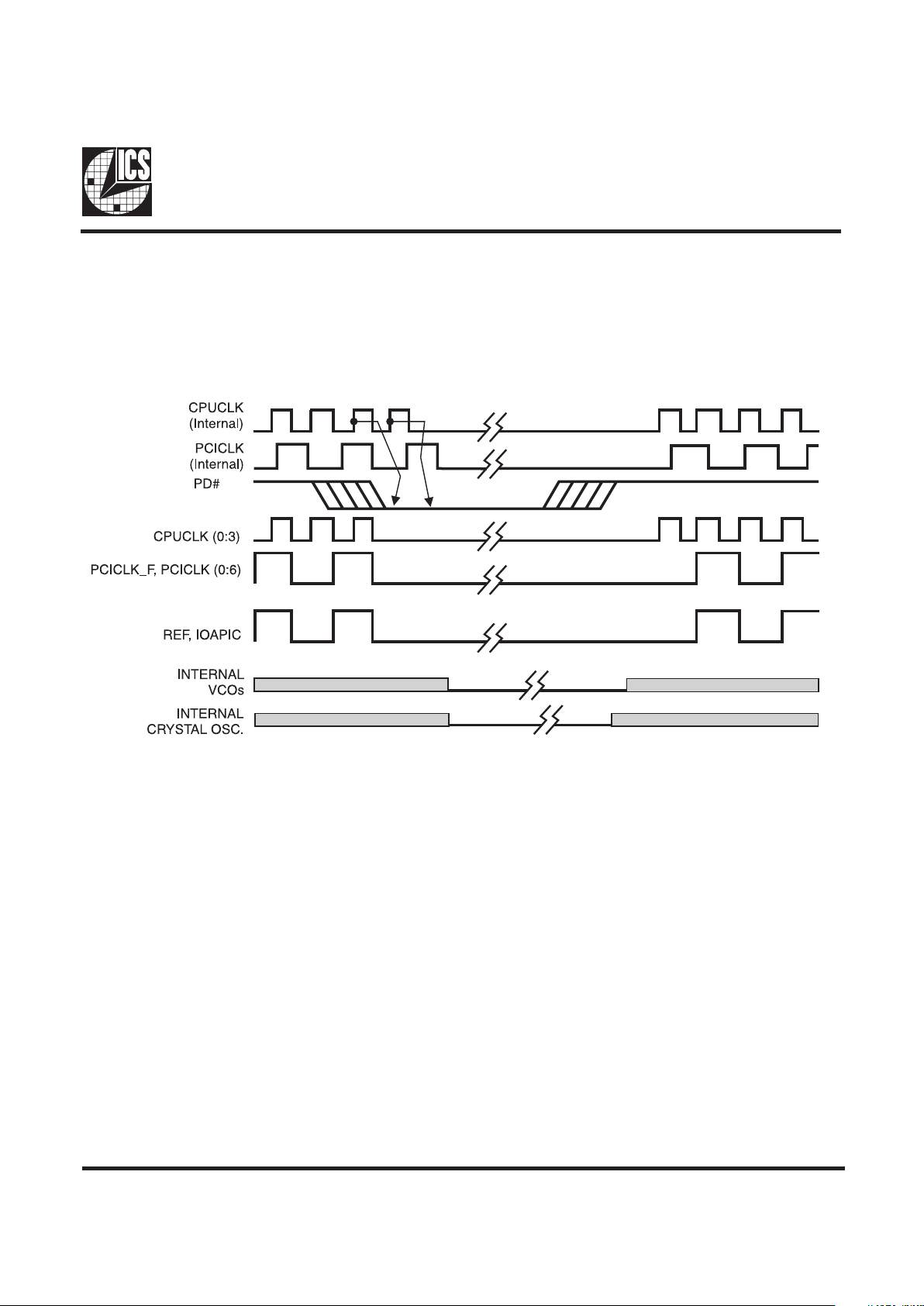
PD# Timing Diagram
The power down selection is used to put the part into a very low power state without turning off the power to the part. PD# is
an asynchronous active low input. This signal is synchronized internally by the ICS9248-55 prior to its control action of
powering down the clock synthesizer. Internal clocks will not be running after the device is put in power down state. When PD#
is active (low) all clocks are driven to a low state and held prior to turning off the VCOs and the Crystal oscillator. The power on
latency is guaranteed to be less than 3ms. The power down latency is less than three CPUCLK cycles. PCI_STOP# and
CPU_STOP# are dont care signals during the power down operations.
Notes:
1. All timing is referenced to the Internal CPUCLK (defined as inside the ICS9248 device).
2. PD# is an asynchronous input and metastable conditions may exist. This signal is synchronized inside the ICS9248.
3. The shaded sections on the VCO and the Crystal signals indicate an active clock is being generated.
Page 6
6
ICS9248-55
Absolute Maximum Ratings
Supply Voltage . . . . . . . . . . . . . . . . . . . . . . . . . . 7.0 V
Logic Inputs . . . . . . . . . . . . . . . . . . . . . . . . . . . . GND 0.5 V to VDD +0.5 V
Ambient Operating Temperature. . . . . . . . . . . . 0°C to +70°C
Storage Temperature . . . . . . . . . . . . . . . . . . . . . 65°C to +150°C
Stresses above those listed under Absolute Maximum Ratings may cause permanent damage to the device. These ratings are
stress specifications only and functional operation of the device at these or any other conditions above those listed in the
operational sections of the specifications is not implied. Exposure to absolute maximum rating conditions for extended
periods may affect product reliability.
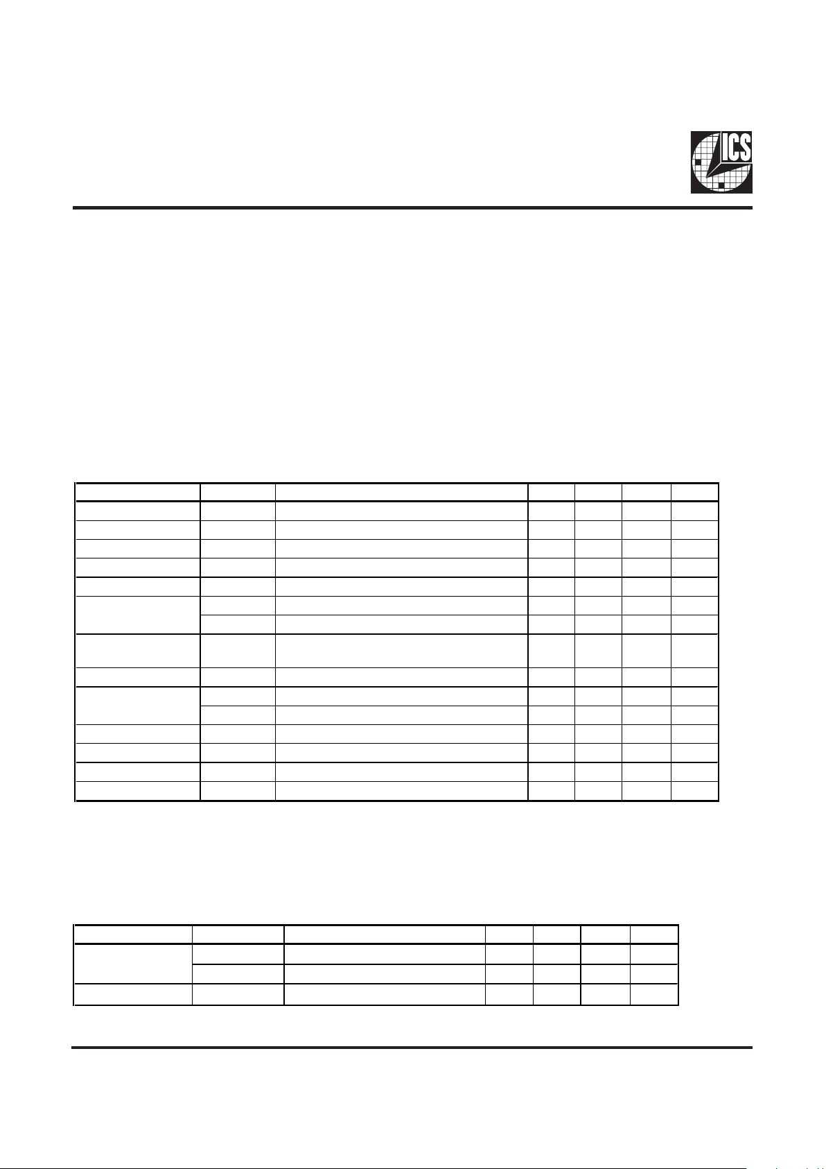
Ele ctrical Chara cteristics - I nput /Supply/ Com m on Out put Par am e t e rs
TA = 0 - 70C ; S upply Voltage VDD = V
DDL
= 3.3 V +/-5% (unles s otherwi se st a t e d)
PARAMETER SYMBOL CONDITIONS MIN TYP MAX UNITS
Input High Voltage V
IH
2V
DD
+0.3 V
Input Low Voltage V
IL
VSS-0.3 0.8 V
Input High Curre nt I
IH
VIN = V
DD
0.1 5 µA
Input Low Current I
IL1
VIN = 0 V; I nputs with no pull- up res is tors - 5 2.0 µA
Input Low Current I
IL2
VIN = 0 V; I nputs with pull- up res istors -200 -100 µA
Operating I
DD3.3OP66CL
= 0 pF ; Selec t @ 66MHz 60 170 m A
Supply Curr ent I
DD3.3OP100CL
= 0 pF ; Selec t @ 100MHz 66 170 m A
Power Down
Supply Curr ent
I
DD3.3PD
CL = 0 pF ; With input addr e ss to V dd or G ND 70 600 µA
Input fr e quenc y F
i
VDD = 3.3 V; 11 14.318 16 MHz
C
IN
Logic I nputs 5 pF
C
INX
X1 & X 2 pins 27 36 45 pF
Transition Time
1
T
trans
To 1st crossing of target Fre q. 3 ms
Settli ng Ti m e
1
T
s
From 1s t crossing to 1% tar ge t Fr eq. 5 ms
Clk Stabilization
1
T
STAB
From VDD = 3.3 V to 1% ta rget F req. 3 ms
Skew
1
T
CPU-PCI1VT
= 1.5 V; 1.5 3 4 ns
1
Gua rantee d by design, not 100% tested in production.
Input C a pacitance
1
Electri cal Character i sti cs - I nput/ Supply/Com mon O utput Paramet ers
TA = 0 - 70C; Supply Voltage VDD = 3.3 V + /-5% , V
DDL
= 2. 5 V +/- 5% ( unl es s otherw ise st at ed)
PARAMETER SY MBOL CO ND ITIO NS MIN TYP MAX UNI TS
Ope r a ting I
D D2.5OP66
CL = 0 pF; Selec t @ 66. 8 MHz 16 72 mA
Suppl y C urrent I
DD2.5OP100
CL = 0 pF; S ele c t @ 100 M H z 23 100 m A
Skew
1
t
CPU-PCI2
VT = 1.5 V; VTL = 1.25 V
1.5 3 4 ns
1
G ua rante e d by d e sign, not 100% test e d in production .
Page 7
7
ICS9248-55
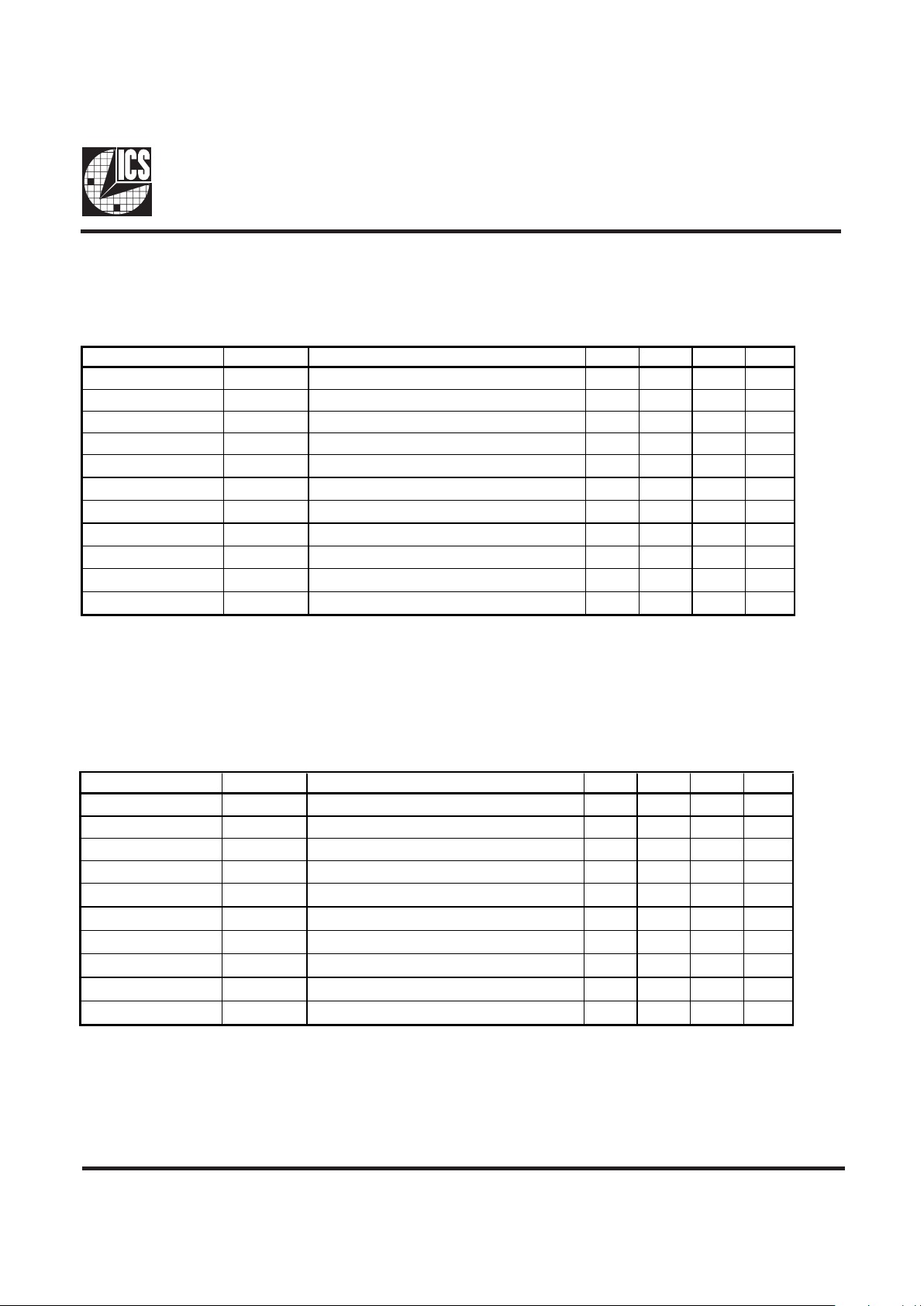
Electri cal Characteri st i cs - CPUCLK
TA = 0 - 70C; VDD = 3.3 V + /-5%, V
DDL
= 2.5 V +/- 5% ; CL = 10 - 20 pF (u nle ss ot h erwis e state d)
PARAMETER SY MBOL CO ND ITI ON S MIN TYP MAX UN ITS
Output High Voltage V
OH2B
IOH = -12. 0 mA 2 2.3 V
Output Low Voltage V
OL2B
IOL = 12 mA 0.2 0.4 V
O utput High Curr e nt I
OH2B
VOH = 1 .7 V - 41 - 19 m A
Ou tput Low Cu rrent I
OL2B
VOL = 0.7 V 19 37 mA
Rise Time t
r2B
1
VOL = 0.4 V, VOH = 2.0 V 1.25 1.6 ns
Fall Time t
f2B
1
VOH = 2.0 V, VOL = 0 .4 V 1 1.6 ns
Duty Cycle d
t2B
1
VT = 1.25 V 454855%
Skew t
sk2B
1
VT = 1.25 V 30 175 ps
Jitter, C ycle -to-c ycle t
j
cyc-cyc2B
1
VT = 1.25 V 150 200 ps
Jitter, One Sigma t
j
1s2B
1
VT = 1.25 V 40 150 ps
Jitter, Absolute
t
jabs2B
1
VT = 1.25 V
-2 50 140 +250 ps
1
G ua ranteed by design, not 100% t e sted in production.
Electrical Characterist ics - I O A PIC
TA = 0 - 70C; VDD = 3.3 V + /-5%, V
DDL
= 2. 5 V +/-5% ; CL = 20 pF
PARA METER SYMBOL COND ITIO N S MIN TYP MAX UN ITS
Output High Voltage V
OH4B
IOH = -18 m A 2 2.2 V
Output Low Voltage V
OL4B
IOL = 18 mA 0.33 0.4 V
O utput High Cur rent I
OH4B
VOH = 1 .7 V -41 - 28 m A
Ou tput L o w Curr e nt I
OL4B
VOL = 0.7 V 29 37 mA
Rise Time
1
T
r4B
VOL = 0.4 V , VOH = 2.0 V 1.5 2 ns
Fa ll T ime
1
T
f4B
VOH = 2.0 V, VOL = 0.4 V 1.3 2 ns
Duty Cycle
1
D
t4B
VT = 1.25 V 455455%
Skew
1
t
sk4B
1
VT = 1.25 V 60 250 ps
Jitter, One Sigm a
1
T
j1s4B
VT = 1.25 V 1 3 %
Jitter, Absolute
1
T
jabs4B
VT = 1.25 V
-5 5 %
1
G uaranteed by des ign, not 100% te s te d in production.
Page 8
8
ICS9248-55
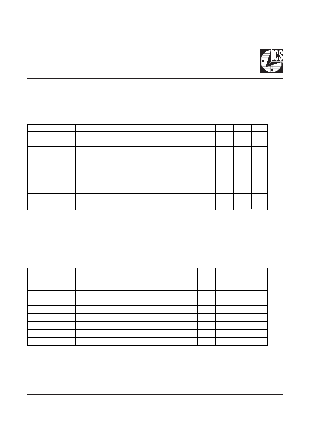
Electrical Character isti cs - PCICLK
TA = 0 - 70C; VDD = V
DDL
= 3.3 V +/-5%; CL = 30 pF
PARA METER SYMBOL COND ITIO N S MIN TYP MAX UN ITS
Output High Voltage V
OH1
IOH = -11 m A 2.4 3.1 V
Output Low Voltage V
OL1
IOL = 9. 4 mA 0.1 0.4 V
O utput High Cur rent I
OH1
VOH = 2 . 0 V -62 -22 m A
O utput L o w Cu rre nt I
OL1
VOL = 0. 8 V 16 57 m A
Rise Time
1
t
r1
VOL = 0. 4 V, VOH = 2.4 V 1.5 2 ns
Fa ll T ime
1
t
f1
VOH = 2.4 V, VOL = 0.4 V 1.1 2 ns
Duty Cycle
1
d
t1
VT = 1.5 V 455055%
Skew
1
t
sk1
VT = 1.5 V 140 500 ps
Jitter, One Sigm a
1
t
j1s1
VT = 1.5 V 17 150 ps
Jitter, Absolute
1
t
jabs1
VT = 1.5 V
-500 70 500 ps
1
G ua rantee d by d esign, not 100% teste d in production.
Electrical Characteristi cs - REF
TA = 0 - 70C; VDD = V
DDL
= 3.3 V +/-5%; CL = 10 - 20 pF (un less othe rwise s ta te d)
PARA METER SYMBOL COND ITIO N S MIN TYP MAX UN ITS
Output High Voltage V
OH5
IOH = -12 m A 2.6 3.1 V
Output Low Voltage V
OL5
IOL = 9 mA 0.17 0.4 V
O utput High Cur rent I
OH5
VOH = 2 .0 V -44 - 22 m A
O utput L o w Current I
OL5
VOL = 0.8 V 29 42 mA
Rise Time
1
t
r5
VOL = 0.4 V , VOH = 2.4 V 1.4 2 ns
Fa ll T ime
1
t
f5
VOH = 2.4 V, VOL = 0.4 V 1.1 2 ns
Duty Cycle
1
d
t5
VT = 1.5 V 455355%
Jitter, One Sigm a
1
t
j1s5
VT = 1.5 V 1 3 %
Jitter, Absolute
1
t
jabs5
VT = 1.5 V
35%
1
G ua rantee d by d esign, not 100% tes te d in production.
Page 9
9
ICS9248-55
Electrical Characteri stics - 48 M Hz
TA = 0 - 70C; VDD = V
DDL
= 3.3 V +/-5%; CL = 10 - 20 pF (unless othe rw is e stated)
PARA METER SYMBOL COND ITIO N S MIN TYP MAX UN ITS
Frequency Accur a cy
1
F
ACC48m
167 ppm
Output High Voltage V
OH5
IOH = -12 m A 2.6 3 V
Output Low Voltage V
OL5
IOL = 9 mA 0.14 0.4 V
O utput High Cur rent I
OH5
VOH = 2 . 0 V -44 -22 m A
O utput L o w Cu rre nt I
OL5
VOL = 0. 8 V 16 42 m A
Rise Time
1
t
r5
VOL = 0. 4 V, VOH = 2.4 V 1.2 4 ns
Fa ll T ime
1
t
f5
VOH = 2.4 V, VOL = 0.4 V 1.2 4 ns
Duty Cycle
1
d
t5
VT = 1.5 V 455255%
Jitter, One Sigm a
1
t
j1s5
VT = 1.5 V 1 3 %
Jitter, Absolute
1
t
jabs5
VT = 1.5 V
35%
1
G ua rantee d by d esign, not 100% teste d in production.
Page 10
10
ICS9248-55
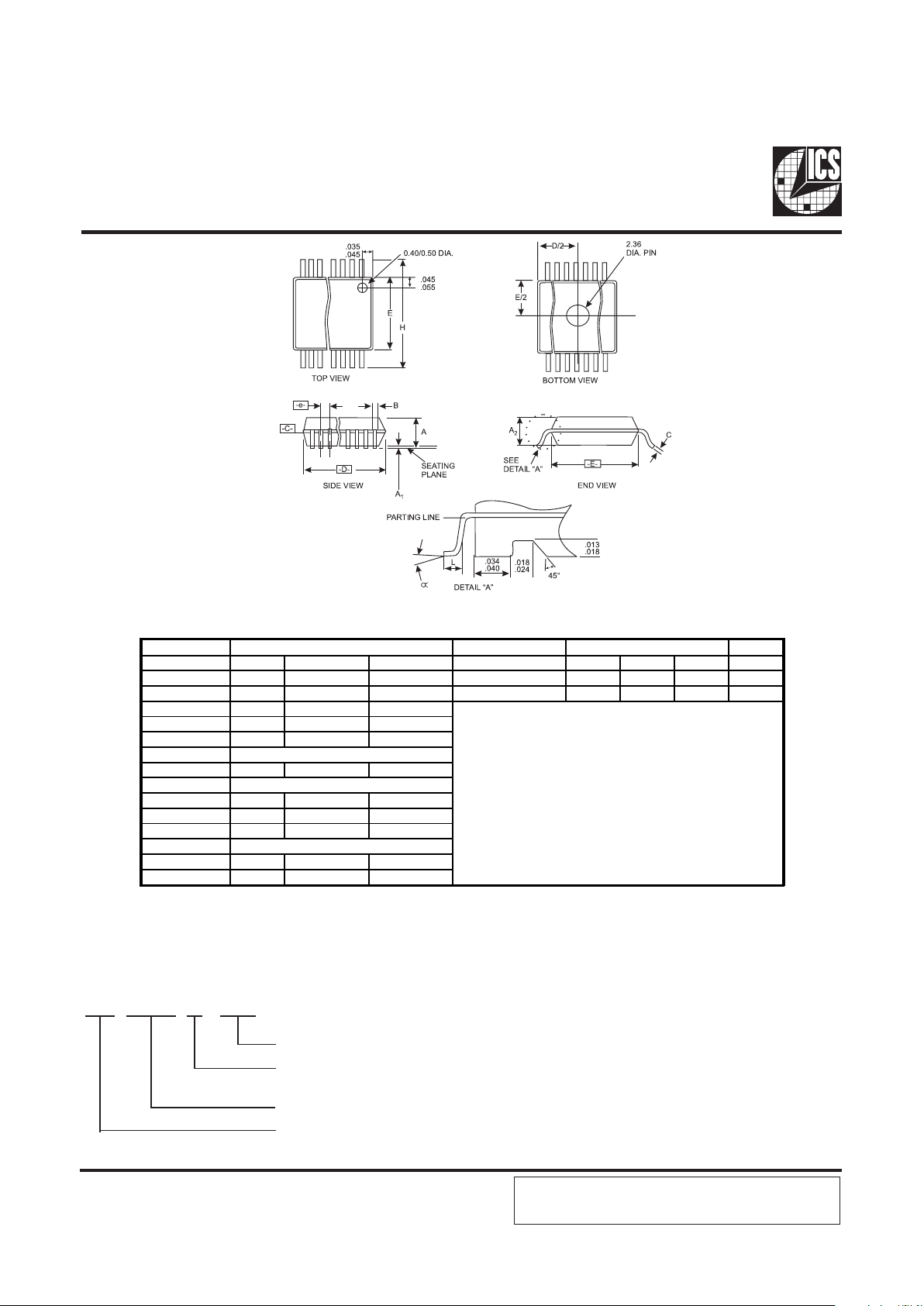
Ordering Information
ICS9248BF-55
Pattern Number (2 or 3 digit number for parts with ROM code patterns)
Package Type
F=SSOP
Device Type (consists of 3 or 4 digit numbers)
Prefix
ICS, AV = Standard Device
Example:
ICS XXXX F - PPP
This table in inches
SSOP Package
SYMBOL COMMON DIMENSIONS VARIATIONS D N
MIN. NOM. MAX. MIN. NOM. MAX.
A .095 .101 .110 AC .620 .625 .630 48
A1 .008 .012 .016 AD .720 .725 .730 56
A2 .088 .090 .092
B .008 .010 .0135
C .005 .006 .0085
D See Variations
E .29 2 .296 .299
e0.025 BSC
H .400 .406 .410
h .010 .013 .016
L .024 .032 .040
N See Variations
∝
0° 5° 8°
X .085 .093 .100
ICS reserves the right to make changes in the device data identified in
this publication without further notice. ICS advises its customers to
obtain the latest version of all device data to verify that any
information being relied upon by the customer is current and accurate.
 Loading...