

Page 1
Integrated
Circuit
Systems, Inc.
General Description Features
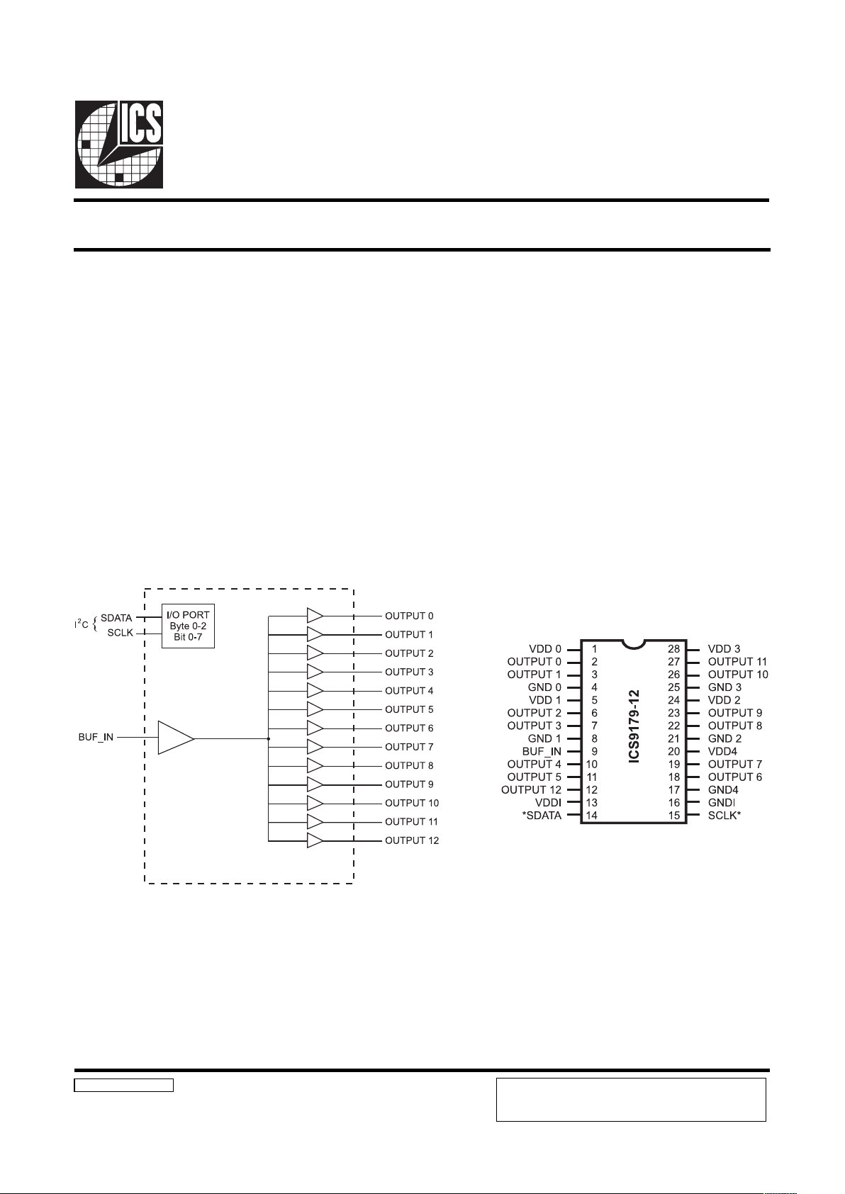
ICS9179-12
Block Diagram
PentiumPro is a trademark of Intel Corporation
I2C is a trademark of Philips Corporation
3 DIMM Buffer
9179-12 Rev C 7/16/99
Pin Configuration
The ICS9179-12 is a buffer intended for reduced pin count
2 - chip Intel BX chipset designs
An I2C interface is included, enabling individual outputs to be
turned on or off. With 13 outputs, up to 3 DIMMs are supported.
Thirteen high speed, low noise buffers, supports up to
three SDRAM DIMMs.
Buffer outputs skew matched to within 250ps.
I
2
C Serial Configuration interface to allow individual
OUTPUTs to be stopped low.
Multiple VDD, VSS pins for noise reduction
3.3V±5% supply voltage
28-pin SOIC and SSOP package
Propagation delay between 1 to 5.5ns
Operation to 133MHz at 3.3V±5%
28-Pin SOIC and SSOP
* Internal pull-up resistor of 100K
Ohms to 3.3V on indicated inputs
PRODUCT PREVIEW documents contain information on new
products in the sampling or preproduction phase of development.
Characteristic data and other specifications are subject to change
without notice.
Power Groups
VDD (0:4), GND (0:4) = Power supply for OUTPUT buffer
VDDI, GNDI = Power supply for I2C circuitry
Page 2
2
ICS9179-12
Pin Descriptions
Notes:
1. At power up all thirteen OUTPUTs are enabled and active.
2. OE has a 100K Ohm internal pull-up resistor to keep all outputs active.
3. The SDATA and SCLK inputs both have internal pull-up resistors with values above 100K Ohms.
REBMUNNIPEMANNIPEPYTNOITPIRCSED
,11,01,7,6,3,2
,32,22,91,81,21
72,62
)21:0(TUPTUOTUOstuptuokcolC
1
9NI_FUBNIsreffubroftupnI
41ATADSO/IIrofnipataD
2
yrtiucricC
3
51KLCSO/IIrofnipkcolC
2
yrtiucricC
3
82,42,02,5,1)4:0(DDVRWPsreffubTUPTUOrofylppusrewoPV3.3
52,12,71,8,4)4:0(DNGRWPsreffubTUPTUOrofdnuorG
31IDDVRWPIrofylppusrewoPV3.3
2
cigollanretnidnayrtiucricC
61IDNGRWPIrofdnuorG
2
cigollanretnidnayrtiucricC
Page 3

3
ICS9179-12
VDD
This is the power supply to the internal core logic of the
device as well as the clock output buffers for OUTPUT (0:12).
This pin operates at 3.3V volts. Clocks from the listed
buffers that it supplies will have a voltage swing from Ground
to this level. For the actual guaranteed high and low voltage
levels for the Clocks, please consult the DC parameter table
in this data sheet.
GND
This is the power supply ground (common or negative) return
pin for the internal core logic and all the output buffers.
OUTPUT (0:12)
These Output Clocks are use to drive Dynamic RAMs and
are low skew copies of the CPU Clocks. The voltage swing
of the OUTPUTs output is controlled by the supply voltage
that is applied to VDD of the device, operates at 3.3 volts.
I
2
C
The SDATA and SCLOCK Inputs are used to program the
device. The clock generator is a slave-receiver device in the
I2C protocol. It will allow read-back of the registers. See
configuration map for register functions. The I2C
specification in Philips I2C Peripherals Data Handbook
(1996) should be followed.
BUF_IN
Input for Fanout buffers (OUTPUT 0:12).
VDDI
This is the power supply to I2C circuitry.
T echnical Pin Function Descriptions
Page 4

4
ICS9179-12
Controller (Host) ICS (Slave/Receiver)
Start Bit
Address
D2
(H)
AC
K
Dummy C ommand Code
AC
K
Dummy Byte Count
AC
K
Byte 0
ACK
Byte 1
AC
K
Byte 2
AC
K
Byte 3
ACK
Byte 4
AC
K
Byte 5
AC
K
Byte 6
ACK
Stop Bit
How to Write:
Controller (Host) ICS (Slave/Receiver)
Start Bit
Address
D3
(H)
ACK
Byte Coun
t
ACK
Byte 0
ACK
Byte 1
ACK
Byte
2
ACK
Byte
3
ACK
Byte
4
ACK
Byte 5
ACK
Byte
6
ACK
Stop Bit
How to Read:
1. The ICS clock generator is a slave/receiver, I2C component. It can read back the data stored in the latches for verification.
Read-Back will support Intel PIIX4 "Block-Read" protocol.
2. The data transfer rate supported by this clock generator is 100K bits/sec or less (standard mode)
3. The input is operating at 3.3V logic levels.
4. The data byte format is 8 bit bytes.
5. To simplify the clock generator I2C interface, the protocol is set to use only "Block-Writes" from the controller. The
bytes must be accessed in sequential order from lowest to highest byte with the ability to stop after any complete byte
has been transferred. The Command code and Byte count shown above must be sent, but the data is ignored for those
two bytes. The data is loaded until a Stop sequence is issued.
6. At power-on, all registers are set to a default condition, as shown.
General I2C serial interface information
The information in this section assumes familiarity with I2C programming.
For more information, contact ICS for an I2C programming application note.
How to Write:
Controller (host) sends a start bit.
Controller (host) sends the write address D2
(H)
ICS clock will acknowledge
Controller (host) sends a dummy command code
ICS clock will acknowledge
Controller (host) sends a dummy byte count
ICS clock will acknowledge
Controller (host) starts sending first byte (Byte 0)
through byte 5
ICS clock will acknowledge each byte one at a time.
Controller (host) sends a Stop bit
How to Read:
Controller (host) will send start bit.
Controller (host) sends the read address D3
(H)
ICS clock will acknowledge
ICS clock will send the byte count
Controller (host) acknowledges
ICS clock sends first byte (Byte 0) through byte 6
Controller (host) will need to acknowledge each byte
Controller (host) will send a stop bit
Notes:
Page 5

5
ICS9179-12
noitidnoC
noitpmusnocylppusV3.3xaM
sdaolpacetercsidxaM
V564.3=DDV
DNGroDDV=stupnicitatsllA
edoMkcolCoN
)DNGro1DDV-NI_FUB(
I
2
evitcAyrtiucriCC
Am3
zHM66evitcA
)zHM66.66=NI_FUB(
Am032
zHM001evitcA
)zHM00.001=NI_FUB(
Am063
zHM331evitcA
)zHM33.331=NI_FUB(
Am005
Byte 1: OUTPUT Clock Register
Functionality
TIB#NIPDWPNOITPIRCSED
7tiB721 )tcanI/tcA(11TUPTUO
6tiB621 )tcanI/tcA(01TUPTUO
5tiB321 )tcanI/tcA(9TUPTUO
4tiB221 )tcanI/tcA(8TUPTUO
3tiB-1 devreseR
2tiB-1 devreseR
1tiB911 )tcanI/tcA(7TUPTUO
0tiB811 )tcanI/tcA(6TUPTUO
ICS9279-12 Power Consumption
The values below are estimates of target specifications.
#EO)31:0(TUPTUO
0Z-iH
1NI_FUBX1
Serial Configuration Command Bitmaps
Byte 0: OUTPUT Clock Register (Default=0)
TIB#NIPDWPNOITPIRCSED
7tiB111 5TUPTUO
6tiB011 4TUPTUO
5tiB
-1
devreseR
4tiB-1
devreseR
3tiB
71
3TUPTUO
2tiB61
2TUPTUO
1tiB31 1TUPTUO
0tiB21 0TUPTUO
Byte 2: OUTPUT Clock Register
TIB#NIPDWPNOITPIRCSED
7tiB-1 devreseR
6tiB211 )tcanI/tcA(21TUPTUO
5tiB-1 devreseR
4tiB-1 devreseR
3tiB-1 devreseR
2tiB-1 devreseR
1tiB-1 devreseR
0tiB-1 devreseR
Notes: 1 = Enabled; 0 = Disabled, outputs held low
Note: PWD = Power-Up Default
Page 6

6
ICS9179-12
Absolute Maximum Ratings
Supply Voltage . . . . . . . . . . . . . . . . . . . . . . . . . . 7.0 V
Logic Inputs . . . . . . . . . . . . . . . . . . . . . . . . . . . . GND 0.5 V to V
DD
+0.5 V
Ambient Operating Temperature. . . . . . . . . . . . 0°C to +70°C
Storage Temperature . . . . . . . . . . . . . . . . . . . . . 65°C to +150°C
Stresses above those listed under Absolute Maximum Ratings may cause permanent damage to the device. These ratings are
stress specifications only and functional operation of the device at these or any other conditions above those listed in the
operational sections of the specifications is not implied. Exposure to absolute maximum rating conditions for extended
periods may affect product reliability.
Electrical Charact eristics - Input & Supply
TA = 0 - 70C; Supply Voltage VDD = 3 .3 V +/-5% (unless ot h e rwise s t ated)
PARAMETER SYMBOL CONDITIONS MIN TYP MAX UNITS
Input High Voltage V
IH
2V
DD
+0.3 V
Input L ow Volta ge V
IL
VSS-0.3 0.8 V
Inpu t High Cur rent I
IH
VIN = V
DD
5uA
Input Low Current I
IL
VIN = 0 V; Inputs with no pull -up resistor s -5 uA
I
IL
VIN = 0 V; Inputs with 100K pull-up resistor s -60 uA
I
DD1
CL = 0 pF; FIN @ 66MHz 80 120 mA
Operating I
DD2
CL = 0 pF; FIN @ 100MHz 120 180 mA
I
DD3
CL = 0 pF; FIN @ 133MHz 160 250 mA
Suppl y C urrent I
DD4
CL = 30 pF; RS=33Ω; FIN @ 66MHz 180 230 mA
I
DD5
CL = 30 pF; RS=33Ω; FIN @ 100MHz 240 360 mA
I
DD6
CL = 30 pF; RS=33Ω; FIN @ 133MHz 300 500 mA
Input frequen cy F
i
1
VDD = 3.3 V; A ll Outputs Loa de d 10 133 MH z
In put C apacit ance
C
IN
1
Logic Inputs 5 pF
1
G ua renteed by de sign, not 100% t este d i n production.
Page 7

7
ICS9179-12
Ele ctrical Characteristics - Outputs
TA = 0 - 70C; VDD = V
DDL
= 3. 3 V +/- 5%; CL = 20 - 30 pF ( unless othe rwise stated)
PARA METER SY MBOL CONDITIONS MIN TYP MAX UNITS
O ut put Impedanc e R
DSP
VO = VDD*(0.5) 10 24
Ω
O ut put Impedanc e R
DSN
VO = VDD*(0.5) 10 24
Ω
O utput High Volta ge V
OH
IOH = -30 mA 2.6 V
Output Low Voltage V
OL
IOL = 23 mA 0.4 V
O utput High Current I
OH
VOH = 2.0 V -54 mA
Ou tput L ow Curr ent I
OL
VOL = 0.8 V 40 mA
Rise Time
1
T
r
VOL = 0.4 V, VOH = 2.4 V 1.33 ns
Fa ll T ime
1
T
f
VOH = 2.4 V, VOL = 0.4 V 1.33 ns
Duty Cycle
1
D
t
VT = 1. 5 V 45 55 %
Skew
1
T
sk
VT = 1. 5 V 250 ps
T
PROP1
VT = 1. 5 V 1 5.5 ns
T
PROP2
VT = 50% BIN to 10% OUT 1 5 ns
Propagation
1
T
PROPE NVT
= 1. 5 V 1 8 ns
T
PROPDISVT
= 1. 5 V
18ns
1
G ua renteed by des ign , not 100% teste d in production.
Page 8
8
ICS9179-12
PRODUCT PREVIEW documents contain information on new
products in the sampling or preproduction phase of development.
Characteristic data and other specifications are subject to change
without notice.
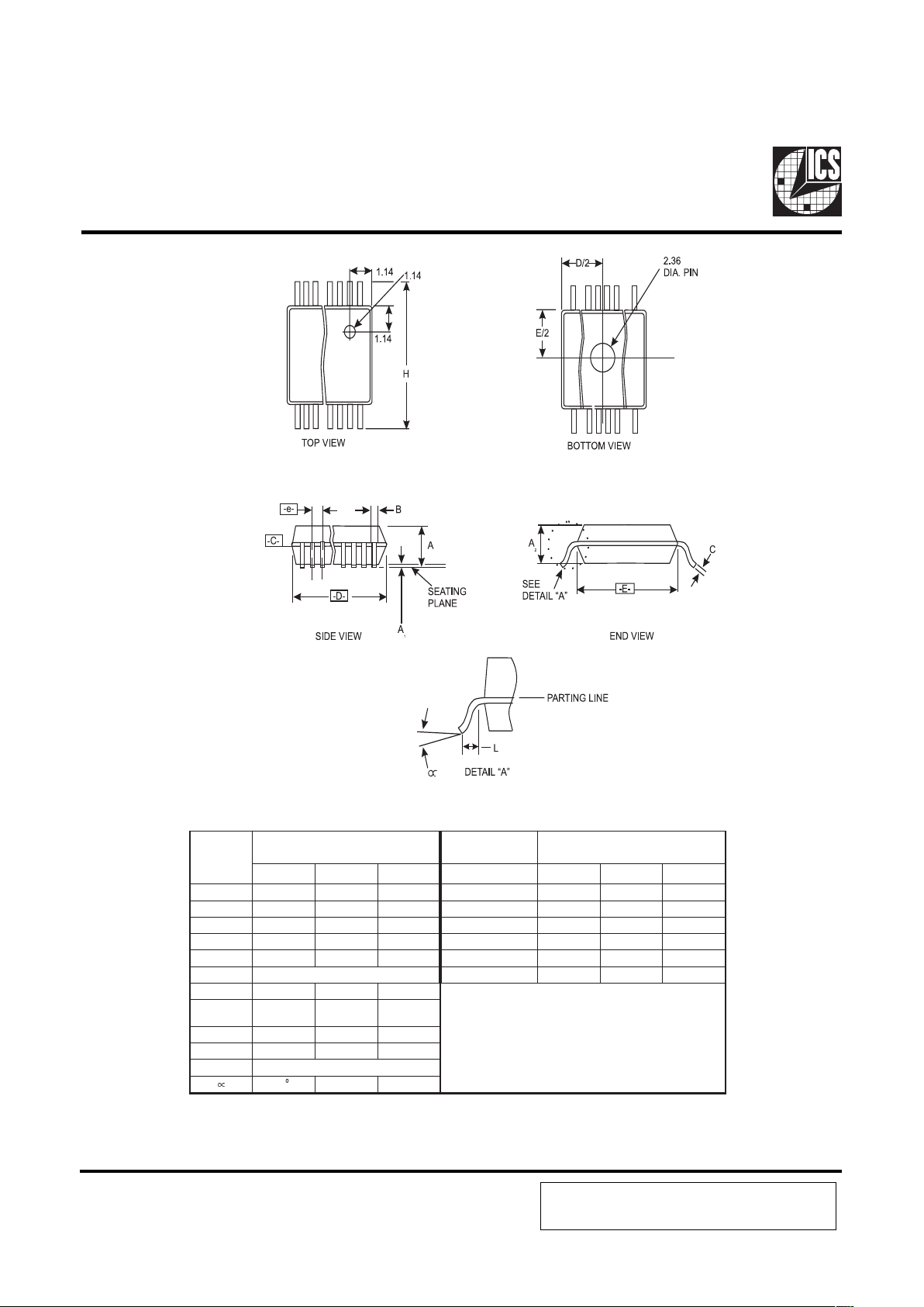
28 Pin SSOP Package
LOBMYS
NOMMOC
SNOISNEMID
SNOITAIRAV
D
.NIM.MON.XAMN .NIM.MON.XAM
A860.0370.0870.041932.0442.0942.0
1A200.0500.0800.061932.0442.0942.0
2A660.0860.0070.002872.0482.0982.0
b010.0210.0510.042813.0323.0823.0
c400.0600.0800.082793.0204.0704.0
DsnoitairaVeeS03793.0204.0704.0
E502.0902.0212.0
e
6520.0
CSB
H103.0703.0113.0
L520.0030.0730.0
NsnoitairaVeeS
µ
°0°4 °8
Page 9
9
ICS9179-12
Ordering Information
ICS9179M-12
Pattern Number (2 or 3 digit number for parts with ROM code patterns)
Package Type
M=SOIC F=SSOP
Device Type (consists of 3 or 4 digit numbers)
Prefix
ICS, AV = Standard Device
Example:
ICS XXXX M - PPP
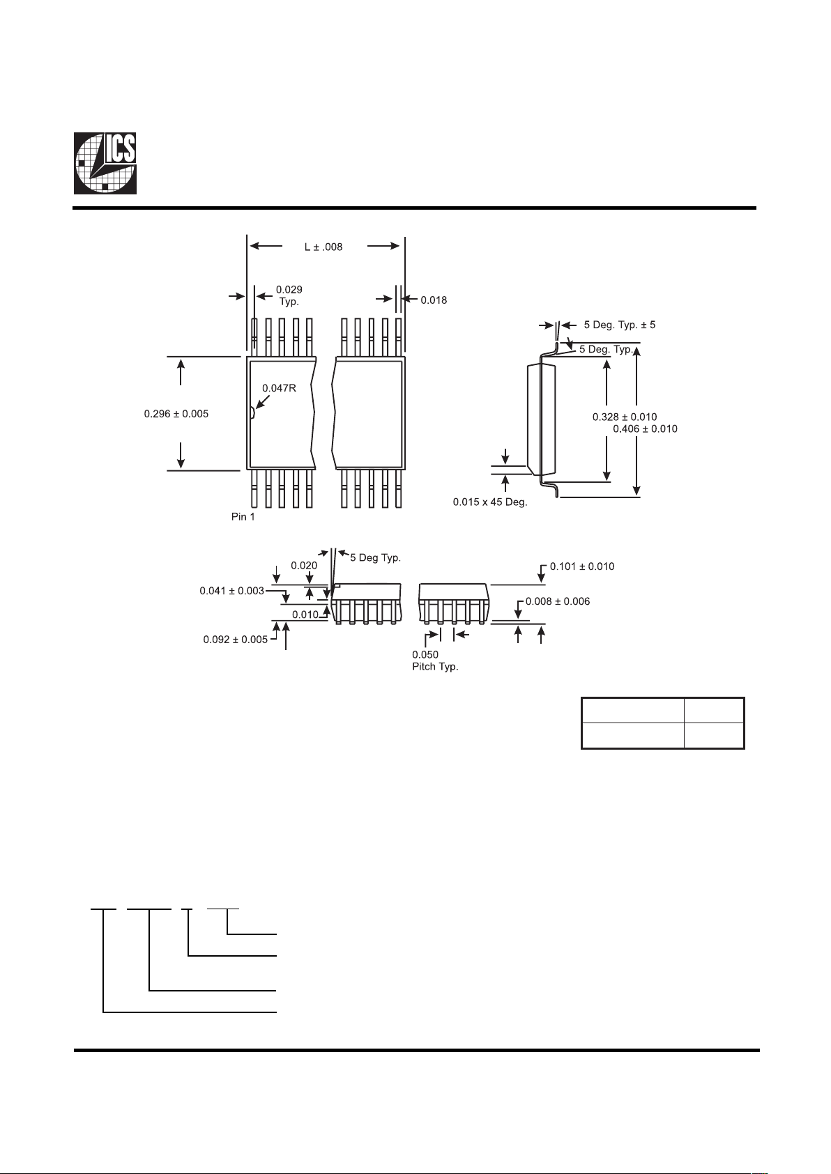
SOIC Package
TNUOCDAELL82
LNOISNEMID407.0
 Loading...