

Page 1
Integrated
Circuit
Systems, Inc.
General Description Features
ICS9179-03
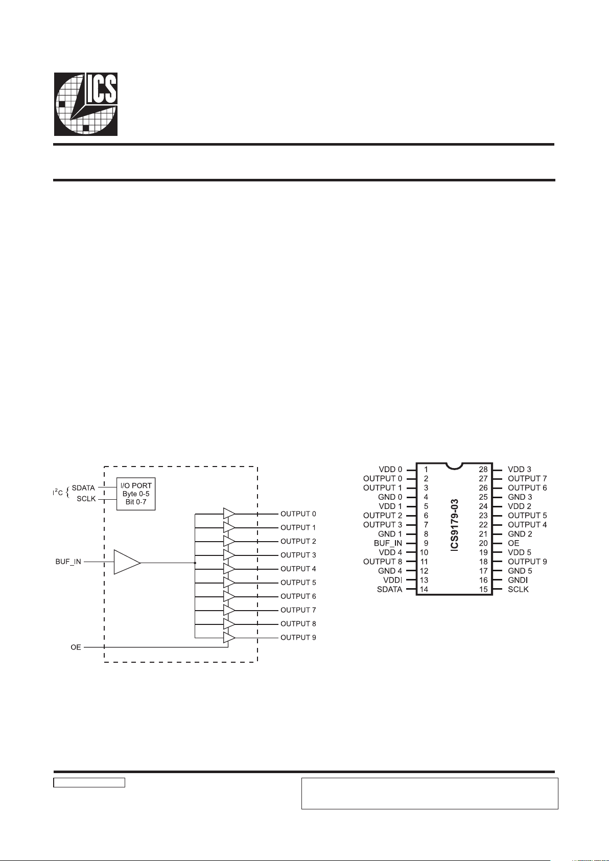
Block Diagram
PentiumPro is a trademark of Intel Corporation
I2C is a trademark of Philips Corporation
Low Skew Fan Out Buffers
9179-03 Rev H 10/16/00
Pin Configuration
The ICS9179-03 generates low skew clock buffers required
for high speed RISC or CISC microprocessor systems such as
Intel PentiumPro. Outputs will handle up to 133MHz clocks.
An output enable is provided for testability.
The device is a buffer with low output to output skew. This is
a Fanout buffer device, not using an internal PLL. This buffer
can also be a feedback to an external PLL stage for phase
synchronization to a master clock. There are a total of ten
outputs, sufficient for feedback to a PLL source and to drive
four small outline DIMM modules (S.O. DIMM) at 2 clocks
each. Or a total of ten outputs as a Fanout buffer from a
common clock source.
The individual clock outputs are addressable through I
2
C to
be enabled, or stopped in a low state for reduced EMI when
the lines are not needed.
Ten High speed, low noise non-inverting buffers for (to
133MHz), clock buffer applications.
Output slew rate faster than 1.5V/ns into 20pF
Supports up to four small outline DIMMS (S.O. DIMM).
Synchronous clocks skew matched to 250ps window on
OUTPUTs (0:9).
I
2
C Serial Configuration interface to allow individual
OUTPUTs to be stopped low.
Multiple VDD, VSS pins for noise reduction
Tri-state pin for testing
3.0V 3.7V supply range
28-pin (209 mil) SSOP and (6.1mm) TSSOP package
28-Pin SSOP & TSSOP
ICS reserves the right to make changes in the device data identified in this
publication without further notice. ICS advises its customers to obtain the latest
version of all device data to verify that any information being relied upon by the
customer is current and accurate.
Page 2
2
ICS9179-03
Pin Descriptions
Power Groups
VDD (0:5), GND (0:5) = Power supply for OUTPUT buffer
VDDI, GNDI = Power supply for I2C circuitry
REBMUNNIPEMANNIPEPYTNOITPIRCSED
3,2)1:0(TUPTUOTUOstuptuokcolC
1
0DNG,0DDVsesu,
7,6)3:2(TUPTUOTUOstuptuokcolC
1
1DNG,1DDVsesu,
32,22)5:4(TUPTUOTUOstuptuokcolC
1
2DNG,2DDVsesu
72,62)7:6(TUPTUOTUOtuptuokcolC
1
3DNG,3DDVsesu
118TUPTUOTUOtuptuokcolC
1
4DNG,4DDVsesu
819TUPTUOTUOtuptuokcolC
1
5DNG,5DDVsesu
9NI_FUBNIsreffubroftupnI
02EONI.pu-lluplanretnisaH.WOLdlehnehwstuptuollasetats-irT
2
41ATADSO/IIrofnipataD
2
yrtiucricC
3
51KLCSO/IIrofnipkcolC
2
yrtiucricC
3
,01,5,1
82,42,91
)5:0(DDVRWPsreffubTUPTUOrofylppusrewoPV3.3
,21,8,4
52,12,71,61
)5:0(DNGRWPsreffubTUPTUOrofdnuorG
31IDDVRWPIrofylppusrewoPV3.3
2
cigollanretnidnayrtiucricC
61IDNGRWPIrofdnuorG
2
cigollanretnidnayrtiucricC
Notes:
1. At power up all ten OUTPUTs are enabled and active.
2. OE has a 100K Ohm internal pull-up resistor to keep all outputs active.
3. The SDATA and SCLK inputs both also have internal pull-up resistors with values above 100K Ohms as well for
complete platform flexibility.
Page 3

3
ICS9179-03
VDD
This is the power supply to the internal core logic of the
device as well as the clock output buffers for OUTPUT (0:9).
This pin operates at 3.3V volts. Clocks from the listed buffers
that it supplies will have a voltage swing from Ground to this
level. For the actual guaranteed high and low voltage levels
for the Clocks, please consult the DC parameter table in this
data sheet.
GND
This is the power supply ground (common or negative) return
pin for the internal core logic and all the output buffers.
OUTPUT (0:9)
These Output Clocks are use to drive Dynamic RAMs and
are low skew copies of the CPU Clocks. The voltage swing of
the OUTPUTs output is controlled by the supply voltage
that is applied to VDD of the device, operates at 3.3 volts.
I
2
C
The SDATA and SCLOCK Inputs are use to program the
device. The clock generator is a slave-receiver device in the
I2C protocol. It will allow read-back of the registers. See
configuration map for register functions. The I2C specification
in Philips I2C Peripherals Data Handbook (1996) should be
followed.
BUF_IN
Input for Fanout buffers (OUTPUT 0:9).
OE
OE tristates all outputs when held low.
VDD1
This is the power supply to I2C circuitry.
Technical Pin Function Descriptions
Page 4

4
ICS9179-03
1. The ICS clock generator is a slave/receiver, I2C component. It can read back the data stored in the latches for verification.
Read-Back will support Intel PIIX4 "Block-Read" protocol.
2. The data transfer rate supported by this clock generator is 100K bits/sec or less (standard mode)
3. The input is operating at 3.3V logic levels.
4. The data byte format is 8 bit bytes.
5. To simplify the clock generator I2C interface, the protocol is set to use only "Block-Writes" from the controller. The
bytes must be accessed in sequential order from lowest to highest byte with the ability to stop after any complete byte
has been transferred. The Command code and Byte count shown above must be sent, but the data is ignored for those
two bytes. The data is loaded until a Stop sequence is issued.
6. At power-on, all registers are set to a default condition, as shown.
General I2C serial interface information
The information in this section assumes familiarity with I2C programming.
For more information, contact ICS for an I2C programming application note.
How to Write:
Controller (host) sends a start bit.
Controller (host) sends the write address D2
(H)
ICS clock will acknowledge
Controller (host) sends a dummy command code
ICS clock will acknowledge
Controller (host) sends a dummy byte count
ICS clock will acknowledge
Controller (host) starts sending first byte (Byte 0)
through byte 5
ICS clock will acknowledge each byte one at a time.
Controller (host) sends a Stop bit
How to Read:
Controller (host) will send start bit.
Controler (host) sends the read address D3
(H)
ICS clock will acknowledge
ICS clock will send the byte count
Controller (host) acknowledges
ICS clock sends first byte (Byte 0) through byte 6
Controller (host) will need to acknowledge each byte
Controller (host) will send a stop bit
Notes:
Controller (Host) ICS (Slave/Receiver)
Start Bit
Address
D2
(H)
AC
K
Dummy Command Code
AC
K
Dummy Byte Count
AC
K
Byte 0
ACK
Byte 1
AC
K
Byte 2
AC
K
Byte 3
ACK
Byte 4
AC
K
Byte 5
AC
K
Byte 6
ACK
Stop Bit
How to Write:
Controller (Host) ICS (Slave/Receiver)
Start Bit
Address
D3
(H)
AC
K
Byte Coun
t
ACK
Byte
0
ACK
Byte 1
ACK
Byte
2
ACK
Byte
3
ACK
Byte
4
ACK
Byte
5
ACK
Byte
6
ACK
Stop Bit
How to Read:
Page 5

5
ICS9179-03
Byte 1: OUTPUT Clock Register
Notes: 1 = Enabled; 0 = Disabled, outputs held low
Byte 2: OUTPUT Clock Register
Notes: 1 = Enabled; 0 = Disabled, outputs held low
TIB#NIPDWPNOITPIRCSED
7tiB811 )tcanI/tcA(9TUPTUO
6tiB111 )tcanI/tcA(8TUPTUO
5tiB-1 devreseR
4tiB-1 devreseR
3tiB-1 devreseR
2tiB-1 devreseR
1tiB-1 devreseR
0tiB-1 devreseR
TIB#NIPDWPNOITPIRCSED
7tiB721 )tcanI/tcA(7TUPTUO
6tiB621 )tcanI/tcA(6TUPTUO
5tiB321 )tcanI/tcA(5TUPTUO
4tiB221 )tcanI/tcA(4TUPTUO
3tiB-1 devreseR
2tiB-1 devreseR
1tiB-1 devreseR
0tiB-1 devreseR
ICS9179-03 Power Management
The values below are estimates of target specifications.
Note: PWD = Power-Up Default
Serial Configuration Command Bitmaps
Byte 0: OUTPUT Clock Register (Default=0)
Notes: 1 = Enabled; 0 = Disabled, outputs held low
Note: PWD = Power-Up Default
TIB#NIPDWPNOITPIRCSED
7tiB-1 devreseR
6tiB-1 devreseR
5tiB
-1
devreseR
4tiB-1
devreseR
3tiB
71
3TUPTUO
2tiB61
2TUPTUO
1tiB31 1TUPTUO
0tiB21 0TUPTUO
Functionality
#EO)9:0(TUPTUO
0Z-iH
1NI_FUBX1
noitidnoC
noitpmusnocylppusV3.3xaM
sdaolpacetercsidxaM
V564.3=DDV
DNGroDDV=stupnicitatsllA
edoMkcolCoN
)DNGro1DDV-NI_FUB(
I
2
evitcAyrtiucriCC
Am3
zHM66evitcA
)zHM66.66=NI_FUB(
Am032
zHM001evitcA
)zHM00.001=NI_FUB(
Am063
zHM331evitcA
)zHM33.331=NI_FUB(
Am064
Page 6

6
ICS9179-03
Absolute Maximum Ratings
Supply Voltage . . . . . . . . . . . . . . . . . . . . . . . . . . . 7.0 V
Logic Inputs . . . . . . . . . . . . . . . . . . . . . . . . . . . . GND 0.5 V to V
DD
+0.5 V
Ambient Operating Temperature . . . . . . . . . . . . 0°C to +70°C
Storage Temperature . . . . . . . . . . . . . . . . . . . . . . 65°C to +150°C
Stresses above those listed under Absolute Maximum Ratings may cause permanent damage to the device. These ratings are
stress specifications only and functional operation of the device at these or any other conditions above those listed in the
operational sections of the specifications is not implied. Exposure to absolute maximum rating conditions for extended periods
may affect product reliability.
PARAM ETER SYM B OL CONDITIONS MIN TYP MAX UNITS
Input High Voltage V
IH
2V
DD
+0.3 V
Input Low Voltage V
IL
VSS-0.3 0.8 V
Input High Current I
IH
VIN = V
DD
5uA
Input Low Current I
IL
VIN = 0 V; Inputs with no pull-up resistors -5 uA
I
IL
VIN = 0 V; Inputs with 100K pull-up resistors -60 -33 uA
I
DD1
CL = 0 pF; FIN @ 66M 80 120 mA
Operating I
DD2
CL = 0 pF; FIN @ 100M 120 180 mA
I
DD3
CL = 0 pF; FIN @ 133M 170 240 mA
Supply Current I
DD4
CL = 30 pF; RS=33Ω; FIN @ 66M 180 260 mA
I
DD5
CL = 30 pF; RS=33Ω; FIN @ 100M 240 360 mA
I
DD6
CL = 30 pF; RS=33Ω; FIN @ 133M 350 460 mA
Input frequency F
i
1
VDD = 3.3 V; All Outputs Loaded 10 133 MHz
Input Capacitance
C
IN
1
Logic Inputs 5 pF
1
Guarenteed by design, not 100% tested in production.
Page 7

7
ICS9179-03
Electrical Characteristics - Outputs
TA = 0 - 70C; VDD = 3.3 V +/-5%; CL = 20 - 30 pF (unless otherwise stated)
PARAM ETER SYM B OL CONDITIONS MIN TYP MAX UNITS
Output Impedance R
DSP
VO = VDD*(0.5) 10 24
Ω
Output Impedance R
DSN
VO = VDD*(0.5) 10 24
Ω
Output High Voltage V
OH
IOH = -30 mA 2.3 3 V
Output Low Voltage V
OL
IOL = 23 mA 0.27 0.4 V
Output High Current I
OH
VOH = 2.0 V -115 -54 mA
Output Low Current I
OL
VOL = 0.8 V 40 57 mA
Rise Time
1
T
r
VOL = 0.4 V, VOH = 2.4 V 0.95 1 .3 3 ns
Fall Time
1
T
f
VOH = 2.4 V, VOL = 0.4 V 0.95 1 .3 3 ns
Duty Cycle
1
D
t
VT = 1.5 V 455055%
Skew
1
T
sk
VT = 1.5 V 110 250 ps
T
PHL1
VT = 1.5 V 1 5.2 5.5 ns
T
PLH1
VT = 1.5 V 1 5.2 5.5 ns
Propagation
1,2
T
PHL2
50% Buffer In to 90% Out 1 4.3 5 ns
T
PLH2
50% Buffer In to 10% Out 1 4.3 5 ns
T
EN
VT = 1.5 V 1 8 ns
T
DIS
VT = 1.5 V
18ns
Note2: Duty cycle of input clock is 47.5% to 52.5%. Input edge rate is for propagation delay
≥
1V/ns
Note1: Paramater is guaranteed by design and characterization for all operating frequencies, (10MHz - 133MHz).
Not 100% tested in production
Page 8

8
ICS9179-03
General Layout Precautions:
1) Use a ground plane on the top layer
of the PCB in all areas not used by
traces.
2) Make all power traces and vias as
wide as possible to lower inductance.
Notes:
1 All clock outputs should have series
terminating resistor. Not shown in all
places to improve readibility of
diagram
2 Optional EMI capacitor should be
used on all CPU, SDRAM, and PCI
outputs.
Capacitor Values:
All unmarked capacitors are 0.01µF ceramic
Page 9

9
ICS9179-03
ICS reserves the right to make changes in the device data identified in this
publication without further notice. ICS advises its customers to obtain the latest
version of all device data to verify that any information being relied upon by the
customer is current and accurate.
Ordering Information
ICS9179yF-03-T
Designation for tape and reel packaging
Pattern Number (2 or 3 digit number for parts with ROM code patterns)
Package Type
F=SSOP
Revision Designator (will not correlate with datasheet revision)
Device Type (consists of 3 or 4 digit numbers)
Prefix
ICS, AV = Standard Device
Example:
ICS XXXX y F - PPP - T
Page 10

10
ICS9179-03
Ordering Information
ICS9179yG-03-T
Designation for tape and reel packaging
Pattern Number (2 or 3 digit number for parts with ROM code patterns)
Package Type
G=TSSOP
Revision Designator (will not correlate with datasheet revision)
Device Type (consists of 3 or 4 digit numbers)
Prefix
ICS, AV = Standard Device
Example:
ICS XXXX y G - PPP - T
6.10 mm. Body, 0.65 mm. pitch TSSOP
(240 mil)
(0.0256 mil)
MIN MAX MIN MAX
A - 1.20 - .047
A1 0.05 0.15 .002 .006
A2 0.80 1.05 .032 .041
b 0.19 0.30 .007 .012
c 0.09 0.20 .0035 .008
D
E
E1 6.00 6.20 .236 .244
e 0.65 BASIC 0.0256 BASIC
L 0.45 0.75 .018 .030
N
α
0° 8° 0° 8°
aaa - 0.10 - .004
VARIATIONS
MIN MAX MIN MAX
28 9.60
9.80
.378 .386
MO-153 JEDEC
Doc.# 10-0038
7/6/00 Rev B
N
D mm.
D (inch)
SEE VARIATIONS
SYMBOL
SEE VARIATIONS
SEE VARIATIONS
In Millimeters
COMMON DIMENSIONS
In Inches
COMMON DIMENSIONS
SEE VARIATIONS
8.10 BASIC 0.319
 Loading...