

Page 1
Integrated
Circuit
Systems, Inc.
General Description Features
ICS9179-06
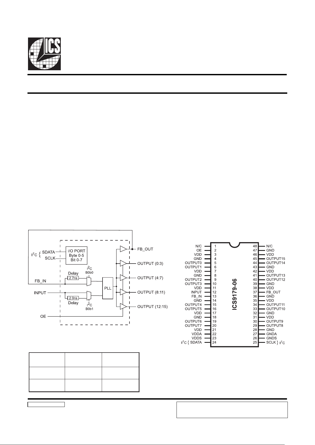
Block Diagram
PentiumPro is a trademark of Intel Corporation
I2C is a trademark of Philips Corporation
Zero Delay Buffers
9179-06 Rev F 6/22/99
Pin Configuration
The ICS9179-06 generates low skew clock buffers required
for high speed RISC or CISC microprocessor systems such as
Intel PentiumPro. An output enable is provided for testability.
The device is a buffer with low output to output skew. This is
a zero delay buffer device, using an internal PLL. This buffer
can be used for phase synchronization to a master clock. With
the wide PLL loop BW, this buffer is compatible to Spread
Spectrum input clocks from clock generator products such as
the ICS9148-27.
The individual clock outputs are addressable through I2C to be
enabled, or stopped in a low state for reduced EMI when the
lines are not needed. The device defaults to zero-delay mode,
but can be programmed with I2C for selectable delays -2.7,
+2.0, -0.7 ns (nominal target values).
Zero delay buffer, 16 outputs
Supports up to four SDRAM DIMMS
Wide PLL loop bandwidth makes this part ideal in
Spread Spectrum applications.
Skew Input to FB_IN ±250ps default, with selectable
skew -2.7, +2.0, -0.7ns nominal.
Synchronous clocks skew matched to 250ps window on
output.
33 to 133MHz input or output frequency.
I
2
C Serial Configuration interface to allow individual
clocks to be stopped, or selectable delays.
Multiple VDD, VSS pins for noise reduction
Slew rate 1.5V/ns into 30pF.
VDD = 3.3 ±5%, 0 to 70°C
All outputs (0:15) tristate with OE low
(FB_OUT stays running).
48-Pin SSOP package
48-Pin SSOP
ICS reserves the right to make changes in the device data identified in
this publication without further notice. ICS advises its customers to
obtain the latest version of all device data to verify that any
information being relied upon by the customer is current and accurate.
Functionality
#EO
TUPTUO
)51:0(
TUO_BF
0Z-iHTUPNIX1
1TUPNIX1TUPNIX1
Page 2
2
ICS9179-06
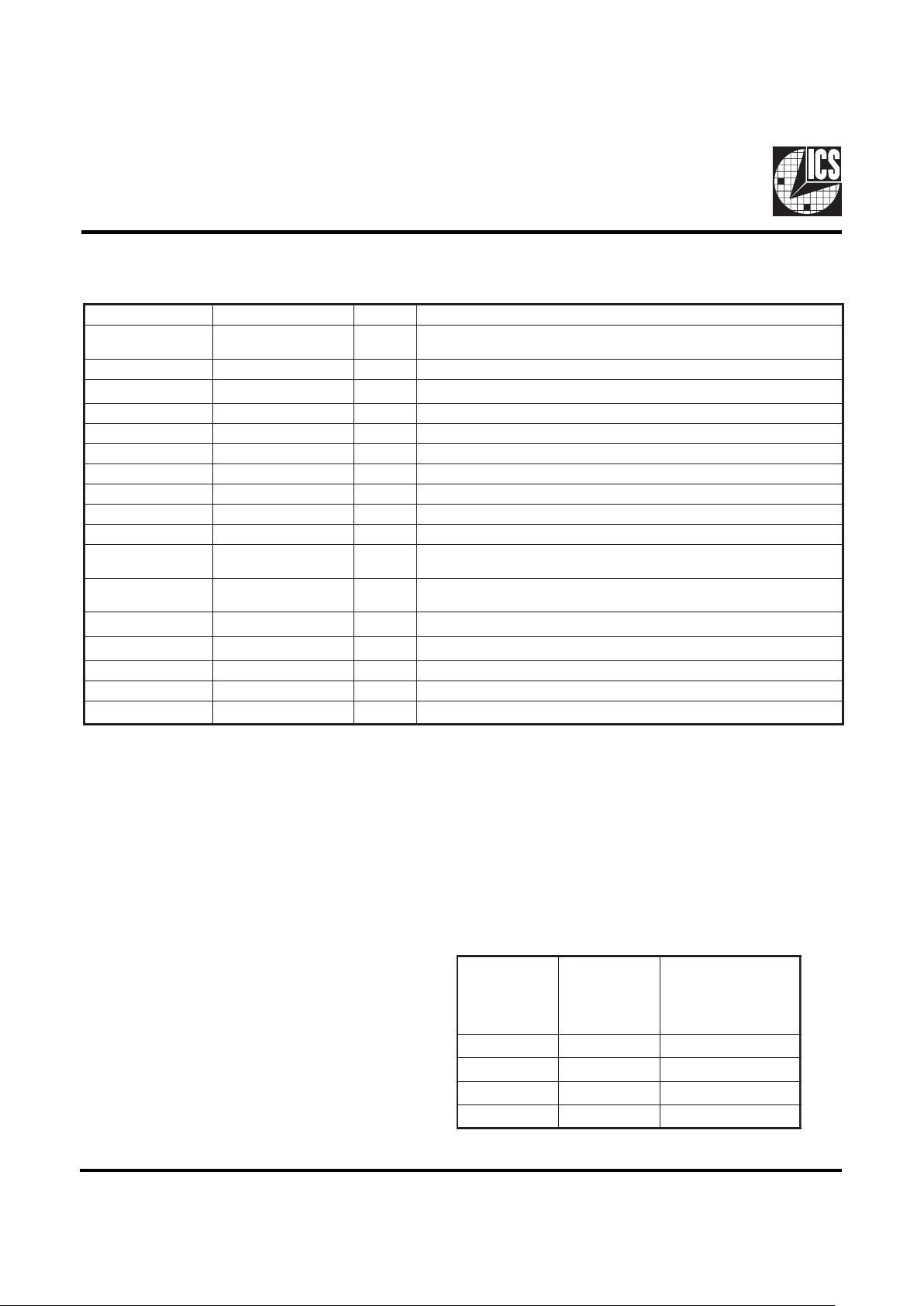
Pin Descriptions
Power Groups
VDD = Power supply for OUTPUT buffers
VDDS = Power supply for I2C circuitry
VDDA = Power supply for Analog PLL circuitry
Notes:
1. At power up all sixteen outputs are enabled and active.
2. OE has a 100K Ohm internal pull-up resistor to keep all outputs active.
3. The SDATA and SCLK inputs both also have internal pull-up resistors with values above 100K Ohms as well for
complete platform flexibility.
4. I2C Byte0, bits 0 & 1 used to select delay. Default* values at power up is 0
5. Subject to design engineering verification of target value.
REBMUNNIPEMANNIPEPYTNOITPIRCSED
2EONI
lanretnisaH.WOLdlehnehwTUO_BFtpecxestuptuollasetats-irT
.pu-llup
2
01,9,6,5)3:0(TUPTUOTUOstuptuokcolc0etyBMARDS
1
02,91,61,51)7:4(TUPTUOTUOstuptuokcolc1etyBMARDS
1
43,33,03,92)11:8(TUPTUOTUOstuptuokcolc2etyBMARDS
1
54,44,14,04)51:21(TUPTUOTUOstuptuokcolc3etyBMARDS
1
21TUPNINI.kcolcecnereferroftupnI
31NI_BFNI.tupnikcabdeeF
42ATADSO/IIrofnipataD
2
yrtiucricC
3
52KLCSO/IIrofnipkcolC
2
yrtiucricC
3
73TUO_BFTUO.NI_BFtupniottuptuokcabdeeF
,13,12,71,11,7,3
64,24,83,53
DDVRWPsreffubtuptuorofylppusrewoPV3.3
,23,82,81,41,8,4
74,34,93,63
DNGRWPsreffubtuptuorofdnuorG
22ADDVRWPsegatsLLPgolanArofylppusrewoPV3.3
32SDDVRWPIrofylppusrewoPV3.3
2
yrtiucricC
62SDNGRWPIrofdnuorG
2
yrtiucricC
72ADNGRWPsegatsLLPgolanArofdnuorG
84,1C/N- detcennocyllanretnitonerasniP
Ground Groups
GND = Ground supply for OUTPUT buffer
GNDS = Ground supply for I2C circuitry
GNDA = Ground supply for Analog PLL circuitry
Delay Selection Table
4
TUPNI
lortnoC
1tib0etyB
NI_BF
lortnoC
0tib0etyB
tegraTlanimoN
5
otTUPNI,yaleD
.snipNI_BF
*0*0sn0
01 sn7.2-
10 sn0.2+
11 sn7.0-
Page 3
3
ICS9179-06
1. The ICS clock generator is a slave/receiver, I2C component. It can read back the data stored in the latches for verification.
Read-Back will support Intel PIIX4 "Block-Read" protocol.
2. The data transfer rate supported by this clock generator is 100K bits/sec or less (standard mode)
3. The input is operating at 3.3V logic levels.
4. The data byte format is 8 bit bytes.
5. To simplify the clock generator I2C interface, the protocol is set to use only "Block-Writes" from the controller. The
bytes must be accessed in sequential order from lowest to highest byte with the ability to stop after any complete byte
has been transferred. The Command code and Byte count shown above must be sent, but the data is ignored for those
two bytes. The data is loaded until a Stop sequence is issued.
6. At power-on, all registers are set to a default condition, as shown.
General I2C serial interface information
The information in this section assumes familiarity with I2C programming.
For more information, contact ICS for an I2C programming application note.
How to Write:
Controller (host) sends a start bit.
Controller (host) sends the write address D2
(H)
ICS clock will acknowledge
Controller (host) sends a dummy command code
ICS clock will acknowledge
Controller (host) sends a dummy byte count
ICS clock will acknowledge
Controller (host) starts sending first byte (Byte 0)
through byte 5
ICS clock will acknowledge each byte one at a time.
Controller (host) sends a Stop bit
How to Read:
Controller (host) will send start bit.
Controler (host) sends the read address D3
(H)
ICS clock will acknowledge
ICS clock will send the byte count
Controller (host) acknowledges
ICS clock sends first byte (Byte 0) through byte 5
Controller (host) will need to acknowledge each byte
Controller (host) will send a stop bit
Notes:
Controller (Host) ICS (Slave/Receiver)
Start Bit
Address
D3
(H)
AC
K
Byte Count
ACK
Byte
0
ACK
Byte 1
ACK
Byte
2
ACK
Byte
3
ACK
Byte 4
ACK
Byte
5
ACK
Stop Bit
How to Read:
Controller (Host) ICS (Slave/Receiver)
Start Bit
Address
D2
(H)
AC
K
Dummy Command Code
AC
K
Dummy Byte Count
AC
K
Byte 0
AC
K
Byte 1
AC
K
Byte 2
ACK
Byte 3
AC
K
Byte 4
AC
K
Byte 5
AC
K
Stop Bit
How to Write:
Page 4

4
ICS9179-06
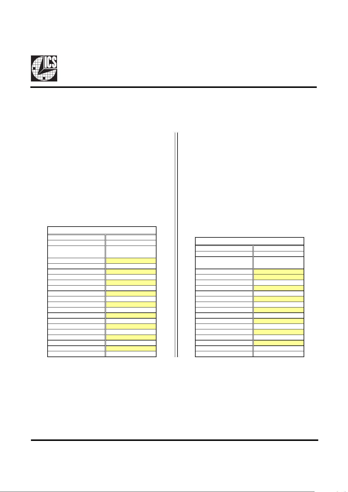
Byte 2: OUTPUT Clock Register (Default = 1)
Notes: 1 = Enabled; 0 = Disabled, outputs held low
TIB#NIPDWPNOITPIRCSED
7tiB541 )tcanI/tcA(51TUPTUO
6tiB441 )tcanI/tcA(41TUPTUO
5tiB141 )tcanI/tcA(31TUPTUO
4tiB041 )tcanI/tcA(21TUPTUO
3tiB431 )tcanI/tcA(11TUPTUO
2tiB331 )tcanI/tcA(01TUPTUO
1tiB031 )evitcanI/evitcA(9TUPTUO
0tiB921 )evitcanI/evitcA(8TUPTUO
Byte 3: OUTPUT Clock Register
Notes: 1 = Enabled; 0 = Disabled, outputs held low
TIB#NIPDWPNOITPIRCSED
7tiB-1 devreseR
6tiB-1 devreseR
5tiB-1 devreseR
4tiB-1 devreseR
3tiB-1 devreseR
2tiB-1 devreseR
1tiB-1 devreseR
0tiB-1 devreseR
ICS9179-06 Power Management
The values below are estimates of target specifications.
noitidnoC
noitpmusnocylppusV3.3xaM
sdaolpacetercsidxaM
V564.3=DDV
DNGroDDV=stupnicitatsllA
edoMkcolCoN
)DNGro1DDV-NI_FUB(
I
2
evitcAyrtiucriCC
Am03
zHM66evitcA
)zHM66.66=NI_FUB(
Am051
zHM001evitcA
)zHM00.001=NI_FUB(
Am081
Note: PWD = Power-Up Default
Byte 0: OUTPUT Clock Register (default = 0)
Notes: 2 = Default = 0; 1 = Delay element enabled,
0 = No delay path.
TIB#NIPDWPNOITPIRCSED
7tiB-0 devreseR
6tiB-0 devreseR
5tiB-0 devreseR
4tiB-0 devreseR
3tiB-0 devreseR
2tiB-0 devreseR
1tiB
2
210 lortnoCwekSTUPNIkcolC
0tiB
2
310 lortnoCwekSNIBF
Serial Configuration Command Bitmaps
Notes: 1 = Enabled; 0 = Disabled, outputs held low
Byte 1: OUTPUT Clock Register
TIB#NIPDWPNOITPIRCSED
7tiB021 )tcanI/tcA(7TUPTUO
6tiB911 )tcanI/tcA(6TUPTUO
5tiB
611
)tcanI/tcA(5TUPTUO
4tiB511
)tcanI/tcA(4TUPTUO
3tiB
011
)tcanI/tcA(3TUPTUO
2tiB91
)tcanI/tcA(2TUPTUO
1tiB61 )tcanI/tcA(1TUPTUO
0tiB51 )tcanI/tcA(0TUPTUO
Note: PWD = Power-Up Default
Page 5

5
ICS9179-06
Absolute Maximum Ratings
Supply Voltage . . . . . . . . . . . . . . . . . . . . . . . . . . 7.0 V
Logic Inputs . . . . . . . . . . . . . . . . . . . . . . . . . . . . GND 0.5 V to VDD +0.5 V
Ambient Operating Temperature. . . . . . . . . . . . 0°C to +70°C
Storage Temperature . . . . . . . . . . . . . . . . . . . . . 65°C to +150°C
Stresses above those listed under Absolute Maximum Ratings may cause permanent damage to the device. These ratings are
stress specifications only and functional operation of the device at these or any other conditions above those listed in the
operational sections of the specifications is not implied. Exposure to absolute maximum rating conditions for extended
periods may affect product reliability.
Electrical Characteristics - Input & Supply
TA = 0 - 70 C; Supply Vol tage VDD = 3.3 V + /- 5% ( unless other wise stated)
PARAMETER SYMBOL CONDITIONS MIN TYP MAX UNITS
Input High Voltage V
IH
2V
DD
+0.3 V
Input L ow V oltage V
IL
VSS-0.3 0.8 V
Input High Current I
IH
VIN = V
DD
5uA
Input L ow Cur r ent I
IL1
VIN = 0 V; I nputs with no pull- up r e s is tor s -5 uA
Input L ow Cur r ent I
IL2
VIN = 0 V; Inputs with pull-up res is tor s -60 -33 uA
O perating I
DD
CL = 0 pF; FIN @ 66M 115 150 mA
Supply C urrent C
L
= 0 pF; FIN @ 100M 170 180 mA
O utput Disabled I
DD
CL = 0 pF; FIN @ 66M 30 m A
Supply C urrent C
L
= 0 pF; FIN @ 100M 30 m A
Input f r eque ncy F
i
VDD = 3. 3 V; All Outputs L oa de d 33 105 MHz
Input C apac itance
C
IN
Logic I nputs 5 pF
1
G ua r e nteed by design, not 100% tes ted in production.
Electri cal Characteri st i cs - I nput & Supply
TA = 0 - 70C; Supply Voltage VDD = 3 .3 V +/-5% (u nle ss othe rw ise stated)
PARAMETER SYMBOL CONDITIONS MIN TYP MAX UNITS
Input High Voltage V
IH
2V
DD
+0.3 V
Input L ow Vol ta ge V
IL
VSS-0.3 0.8 V
Inpu t High Curre nt I
IH
VIN = V
DD
5uA
I
IL
VIN = 0 V; I npu ts wit h no pul l-up r esist ors -5 uA
I
IL
VIN = 0 V; I npu ts wit h 100 K pull-up re sistors - 60 -33 uA
Operating I
DD1
CL = 0 pF; FIN @ 66M 115 150 m A
Suppl y C urrent I
DD2
CL = 0 pF; FIN @ 100M 170 180 m A
Input freq uen cy F
i
1
VDD = 3.3 V; All O ut puts L o ade d 10 150 MHz
In put Capacitance
C
IN
1
Logic Inputs 5 pF
1
G ua rentee d by de sign, no t 100 % teste d i n production.
Input Low Current
Page 6

6
ICS9179-06
PARA METER SYMBOL COND ITIO NS MIN TYP MAX UNI TS
O ut put Fr e qu e ncy F
O3
33 133 MHz
Ou tput Impe da nc e R
DSP3
VO = VDD*(0.5) 10 24 Ohm
Ou tput Impe da nc e R
DSN3
VO = VDD*(0.5) 10 24 Ohm
Output High Voltage V
OH3
IOH = -30 mA 2.6 V
Output Low Voltage V
OL3
IOL = 23 mA 0.4 V
Output High Curr e nt I
OH3
VOH = 2.0 V -54 mA
Output Low Curre nt I
OL3
VOL = 0.8 V 40 mA
Rise Time T
r3
VOL = 0.4 V , VOH = 2.4 V 1.33 nS
Fall Time T
f3
VOH = 2.4 V, VOL = 0.4 V 1.33 nS
Duty Cycle D
t3
VT = 1.5 V 45 55 %
Output to Output
Ske w W i ndo w
T
sk3
VT = 1.5 V 250 pS
T
skd1
VT = 1.5 V default Z e ro delay I2C
B0 bits 0, 1 = 00
-25 0 0 250 pS
IN to FB_IN Skew
1, 2
T
skd2
VT = 1.5 V bi t s 0, 1 = 10 -2.2 -2.7 - 3 .2 nS
T
skd3
VT = 1.5 V bi t s 0, 1 = 01 +1 .5 +2. 0 +2.5 nS
T
skd4
VT = 1.5 V bi t s 0, 1 = 11 -0.2 -0.7 - 1 .2 nS
Electrical Characteri st i cs - SDRAM
TA = 0 - 70C; VDD = V
DDL
= 3.3 V +/- 5%; CL = 20 - 30 pF (unless otherwi se st a t e d)
Notes:
1. Guarenteed by design, not 100% tested in production
2. Delay elements FBIN and clock INPUT path are selected by I2C BYTE2; bit 0 = clock input control, bit 1 = Clock INPUT
Control. (Default is 0). A 0 = No delay in path, 1 = Delay element selected.
Note: PWD = Power-Up Default
Input Pulse
NIMPYTXAMSTINU
esluPtupnI
emiTwoL
T
woL-mi
woL_eslupV ≤ V8.00.1sn
esluPtupnI
emiThgiH
T
hgiH-mi
hgiH_eslupV ≥ V0.25.1sn
Page 7

7
ICS9179-06
General Layout Precautions:
1) Use a ground plane on the top layer
of the PCB in all areas not used by
traces.
2) Make all power traces and vias as
wide as possible to lower inductance.
Notes:
1 All clock outputs should have series
terminating resistor. Not shown in all
places to improve readibility of
diagram
2 Optional EMI capacitor should be
used on all CPU, SDRAM, and PCI
outputs.
Capacitor Values:
All unmarked capacitors are 0.01µF ceramic
Page 8

8
ICS9179-06
Ordering Information
ICS9179F-06
Pattern Number (2 or 3 digit number for parts with ROM code patterns)
Package Type
F=SSOP
Device Type (consists of 3 or 4 digit numbers)
Prefix
ICS, AV = Standard Device
Example:
ICS XXXX F - PPP
SSOP Package
LOBMYS SNOISNEMIDNOMMOC SNOITAIRAV D N
.NIM.MON.XAM.NIM.MON.XAM
A590.101.011.CA026.526.036.84
1A800.210.610.
2A880.090.290.
B800.010.5310.
C500.- 010.
DsnoitairaVeeS
E292.692.992.
eCSB520.0
H004.604.014.
h010.310.610.
L420.230.040.
NsnoitairaVeeS
∝
°0°5°8
X580.390.001.
ICS reserves the right to make changes in the device data identified in
this publication without further notice. ICS advises its customers to
obtain the latest version of all device data to verify that any
information being relied upon by the customer is current and accurate.
 Loading...