

Page 1
Integrated
Circuit
Systems, Inc.
General Description Features
ICS9177
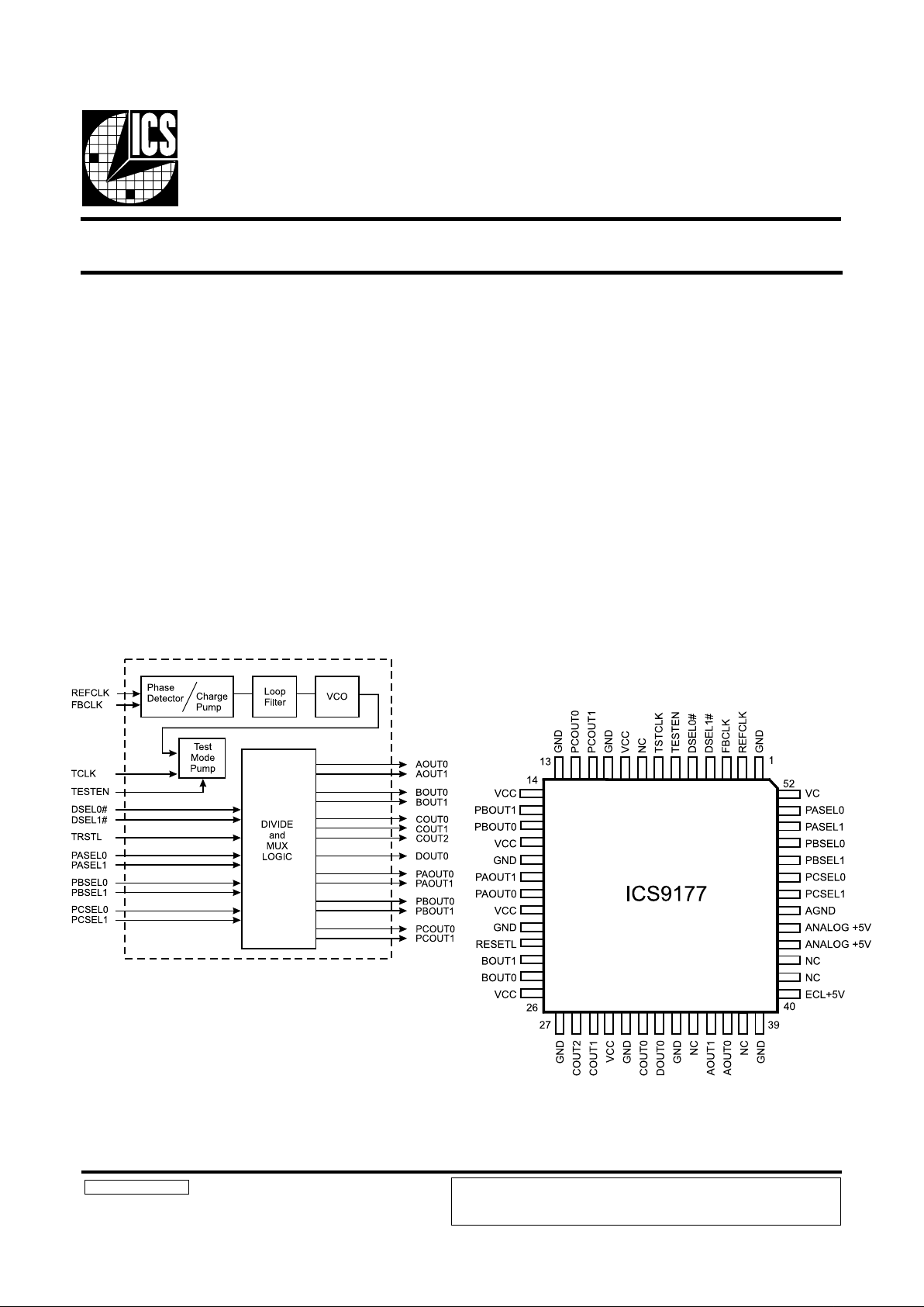
Block Diagram
ICS9177RevB060297P
High Frequency System Clock Generator
The ICS9177 is a multiple output clock generator ideal for
high speed processor system applications. A single highspeed internal VCO is utilized to derive up to four simultaneous
clock output frequencies. This enables output clock skew
matching and the minimization of clock jitter. The internal
VCO operates up to 350 MHz providing edge skew matched
output clocks.
One differential PECL (Positive ECL) output pair provides a
high speed processor clock. 12 TTL clock outputs are also
provided for other system functions, such as bus clocks. Input
selection pins are used to select the TTL output clock
frequencies.
For information about ICS9177 customization optics, please
contact ICS.
• Provides output frequencies up to 175 Mhz
• Internal VCO is divided into four skew-matched output
frequencies (Out A, B, C, D)
• External clock feedback provides input to output skew
matching
• Differential PECL clock output pair provided for high
speed output (Out A)
• 12 TTL clock outputs (for Out B, C, D)
• Single 5 volt power supply voltage
• Internal loop filters
• 52-pin QFP package
Pin Configuration
52-Pin QFP
ICS reserves the right to make changes in the device data identified in this
publication without further notice. ICS advises its customers to obtain the latest
version of all device data to verify that any information being relied upon by the
customer is current and accurate.
Page 2
2
ICS9177
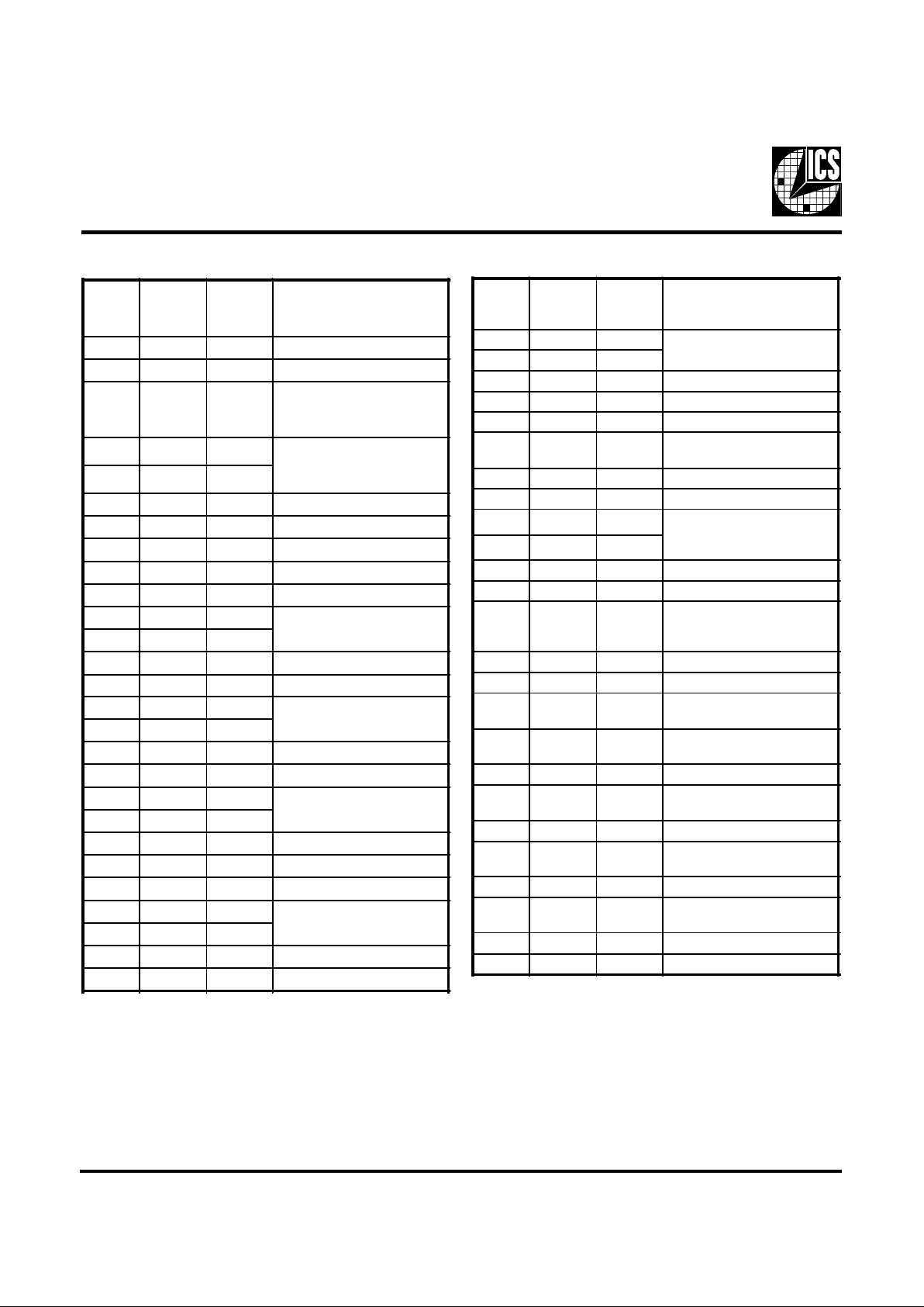
Pin Description
*Internal pull-up resistor
PIN
NUM-
BER
PIN
NAME
TYPE DESCRIPTION
1 GND
2 REFCLK INPUT from external oscillator
3 FBCLK INPUT
external PLL Feedback path
from one of the OutC
outputs
4 DSEL1# INPUT
PLL divider mode control
(Contains i nter nal pul l-up
resistors)
5 DSEL0# INPUT
6 TESTEN INPUT Test mode ENABLE pin
7 TSTCLK INPUT Ext er na l Test Cl k
8NC
9VCC
10 GND
11 PCOUT1 OUTPUT
TTL - Group 2
Programmable clock output s
12 PCOUT0 OUTPUT
13 GND
14 VCC
15 PBOUT1 OUTPUT
TTL - Group 1
Programmable clock output s
16 PBOUT0 OUTPUT
17 VCC
18 GND
19 PAOUT1 OUT PUT
TTL - Group 0
Programmable clock output s
20 PAOUT0 OUT PUT
21 VCC
22 GND
23 RESETL INPUT Low true divider rese t pin
24 BOUT1 OUTP UT
TTL - 50 MHz out put cl ock
25 BOUT0 OUTP UT
26 VCC
27 GND
PIN
NUM-
BER
PIN
NAME
TYPE DESCRIPTION
28 COUT2 OUTPUT
TTL - 25 MHz output clock
29 COUT1 OUTPUT
30 VCC
31 GND
32 COUT0 TTL - 25 MHz output clock
33 DOUT0
TTL - 12.5 MHz output
clock
34 GND
35 NC
36 AOUT1 OUTPUT
ECL - 100 MHz, 75 MHz or
50 MHz based on DSEL(1:0)
pins
37 AOUT0 OUTPUT
38 NC
39 GND
40
ECL+5V
(same as
VCC)
41 NC
42 NC
43
ANALO-
G +5V
44
ANALO-
G +5V
45 AGND
46 PCSEL1 INPUT
Programmable clock Group
C select
47 PCSEL0 INPUT
48 PBSEL1 INPUT
Programmable clock Group
B select
49 PBSEL0 INPUT
50 PASEL1 INPUT
Programmable clock Group
A select
51 PASEL0 INPUT
52 VC
Page 3
3
ICS9177
Function Tables
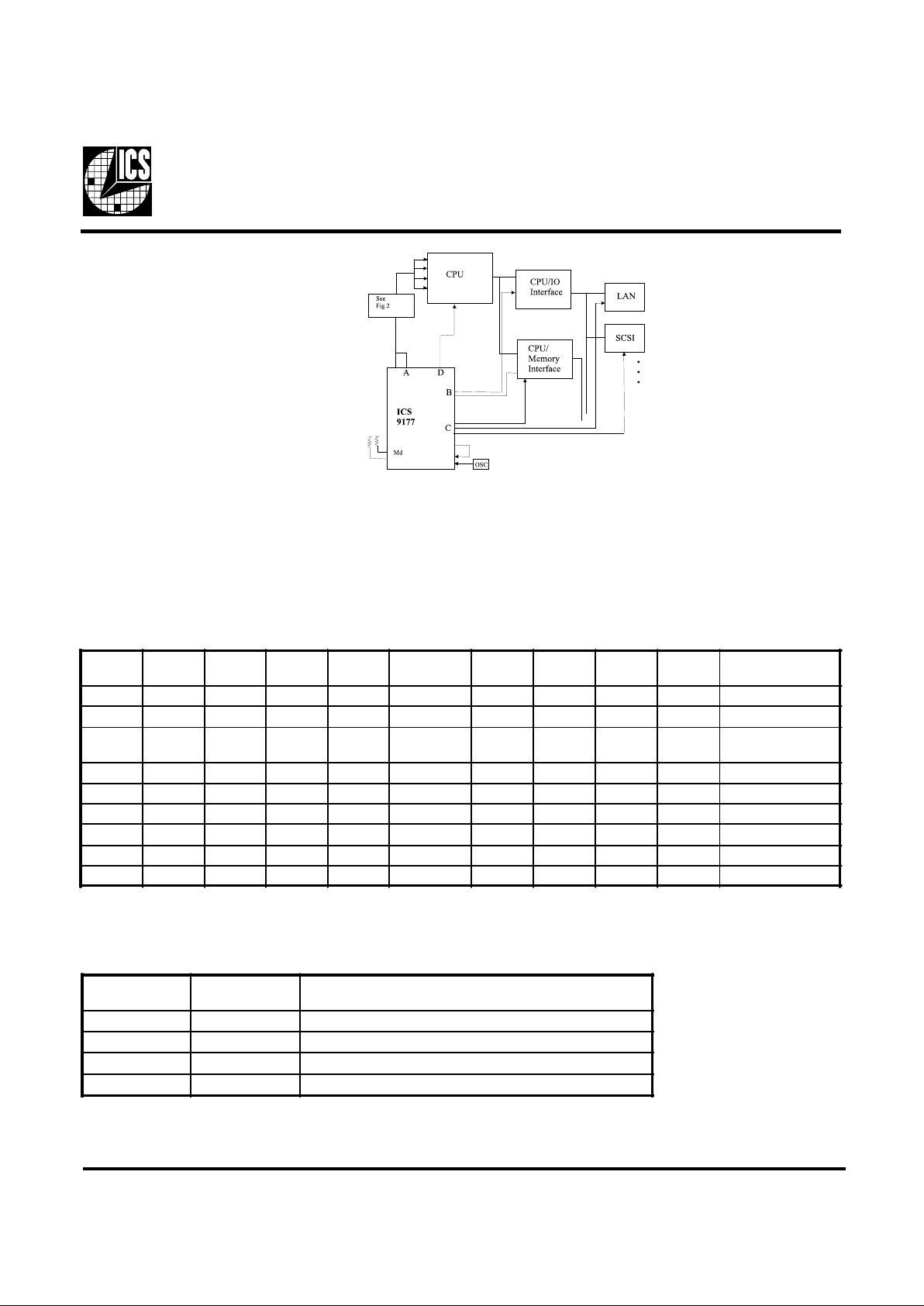
Example of System Block Diagram - Clocking
Table 1: Primary Function Table Typical System Usage
Table 2: CLOCK SELECT Blocks Function Table
Note: x=A, B, or C. (See Figure 1.)
T ypical System Usag e
REF IN
(MHx)
DSEL1# DSEL0# RSTL TEST
f
1
OUT
A
OUT
B
OUT
C
OUT
D
DESCRIPTION
25 0 0 1 0 200 MHz
f/4 f/4 f/8 f/16 Mode 0 - 1/1
25 0 1 1 0 300 M hz
f/4 f/6 f/12 f/24 Mode 1 - 3/2
331010
200/264
MHz
f/2 f/4 f/8 f/16 Mode 2 - 2/1
251110 X 1111Mode 3 - A ll 1
-XX0X X 0000Reset Mode
- 0 0 1 1 TCLK
f/2 f/2 f/4 f/8 Test Mode 0
- 0 1 1 1 TCLK
f/2 f/3 f/6 f/12 Test Mode 1
- 1 0 1 1 TCLK f/1 f/2 f/4 f/8 Test Mode 2
- 1 1 1 1 TCLK f/2 f/2 f/2 f/2 Test Mode 3
PxSEL
1
PxSEL
0
Function of CLOCK SELECT Blocks
0 0 Both outputs at the same frequency as Out B
.
0 1 Both outputs at the same frequency as Out C .
1 0 Both outputs at the same frequency as Out D .
1 1 Both outputs disabled in the high state.
Page 4

4
ICS9177
Note: The arrow indicates the point where the clock sequence starts to repeat.
Clock Output Timing Diagrams
1:1 frequency ratio - Mode 0
3:2 frequency ratio - Mode 1
2:1 frequency ratio - Mode 2
Page 5

5
ICS9177
Absolute Maximum Ratings
Supply voltage . . . . . . . . . . . . . . . . . . . . . . . . . . . . . . 7V
Logic inputs . . . . . . . . . . . . . . . . . . . . . . . . . . . . . . . . GND -.05V to VDD +.05V
Ambient operating temperature . . . . . . . . . . . . . . . . 0°C to +70°C
Storage temperature . . . . . . . . . . . . . . . . . . . . . . . . . . -65°C to +150°C
Stresses above those listed under Absolute Maximum Ratings may cause permanent damage to the device. This is a stress rating
only and functional operation of the device at these or any other conditions above those indicated in the operational sections
of the specifications is not implied. Exposure to absolute maximum rating conditions for extended periods may affect product
reliability.
AC/DC Characteristics
Table 5: AC Specification type Out A.pecl Pins
(CPUCLK)
Test Load Conditions: 100Ω, 15 pF.
Note 1: The pecl levels are standard 10 kHz positive ECL values as shown in the table above.
Note 2: Pin skew and Duty cycle are measured at the signal swing mid-point.
Note 3: The skew and duty cycle numbers reflect the recommended clock distribution method shown in Figure 2
Power Supply Specifications
(Total Power consumption: approximately 750 mw)
Table 3: DC Specifications
A C/DC Input Specification
Table 4: AC Specification of Inputs
Note: tr and tf are typical values for input
Supply I(typ) I(max) V(min) V(typ) V(max)
VDD 150 mA 200 mA 4.75V 5V 5.25V
Pin Type Vih(min) Vil(max) tr tf
All 2V 0.8V 3 3
PARAMETER SYMBOL TEST CONDITIONS MIN TYP MAX UNITS
Output High Voltage
1
Voh 3.87 4.67 volts
Output Low Voltage
1
Vol 2.63 3.19 volts
Output High Current Ioh 38.7 46.7 ma
Output Low Current Iol 26.3 31.9 ma
Rise Time 10-90% tr 1 ns
Fall Time 10-90% tf 1 ns
Duty cycle at 100 MHz 2, 3 dcyc 45 55 %
Page 6

6
ICS9177
Table 6: AC Specification type Out B.ttl Pins
(50 MHz)
Test Load Conditions: 500Ω, 15 pF.
Note 1: Pin skew is measured from the earliest rising edge of the group to the latest rising edge of the group.
Note 2: Delay is the intrinsic delay between the TTL drivers switching and the PECL driver switching. This is measured from
the OutA.pecl signal at the signal swing mid-point to max output of the OutB.ttl signal’s rising edge
Table 7: AC Specification type Out C.ttl Pins
(25 MHz)
Test Load Conditions: 500Ω, 15 pF.
Note 1: Pin skew is measured from the earliest rising edge of the group to the latest rising edge of the group.
Note 2: Spread is the absolute difference between the rising edge of any OutC.ttl signal and the rising edge of any OutB.ttl
signal
PARAMETER SYMBOL TEST CONDITIONS MIN TYP MAX UNITS
Output High Voltage Voh 2.4 3.2 5 volts
Output Low Voltage Vol 0 0.3 0.8 volts
Output High Current Ioh 16 mA
Output Low Current Iol 24 mA
Rise Time 10-90% tr 1 2 3 ns
Fall Time 10-90% tf 1 2 3 ns
Pin skew to other OutB.ttl
signals
1
tsk 250 500 ps
Duty cycle at 1.5V dcyc 45 55 %
Delay from OutA.pecl signals
2
tdly .2 .5 ns
Skew associated with above
delay
3
tdlyskw ±0.5 ns
PARAMETER SYMBOL TEST CONDITIONS MIN TYP MAX UNITS
Output High Voltage Voh 2.4 3.2 5 volts
Output Low Voltage Vol 0 0.3 0.8 volts
Output High Current Ioh 16 mA
Output Low Current Iol 24 mA
Rise Time 10-90% tr 1 2 3 ns
Fall Time 10-90% tf 1 2 3 ns
Pin skew to other OutC.ttl
signals
1
tsk 250 500 ps
Duty cycle at 1.5V dcyc 45 55 %
Spread to OutB.ttl signals
2
tspb 500 ps
Page 7

7
ICS9177
Table 8: AC Specification type Out D.ttl Pins
(12.5 MHz)
Test Load Conditions: 500W, 15 pF.
Note 1: Delay is the intrinsic delay between the TTL drivers switching and the PECL driver switching. This is measured from
the OutA.pecl signal at the signal swing mid-point to max output of the OutD.ttl signal’s rising edge
PARAMETER SYMBOL TEST CONDITIONS MIN TYP MAX UNITS
Output High Voltage Voh 2.4 5 3.2 volts
Output Low Voltage Vol 0 0.8 0.3 volts
Output High Current Ioh 16 mA
Output Low Current Iol 24 mA
Rise Time 10-90% tr 1 3 2 ns
Fall Time 10-90% tf 1 3 2 ns
Pin skew to other OutD.ttl
signals
tsk 500 250 ps
Duty cycle at 1.5V dcyc 45 55 %
Delay from OutA.pecl signals
1
tdly .5 ns
Skew associated with above
delay
2
tdlyskw ±1.3 ns
Page 8

8
ICS9177
Ordering Information
ICS9177-01CF52
Example:
52-Pin QFP Pac kage
ICS XXXX-PPP M X#W
Lead Count & Package Width
Lead Count=1, 2 or 3 digits
W=.3” SOIC or .6” DIP; None=Standard Width
Package Type
F=QFP
Pattern Number (2 or 3 digit number for parts with ROM code patterns)
Device Type (consists of 3 or 4 digit numbers)
Prefix
ICS, A V=Standard Device; GSP=Genlock
LEAD COUNT 44L 52L 64L 80L 100L 64L 80L 100L
BODY THICKNESS 2.0 2.70
FOOTPRINT (BODY+) 3.20
DIMENSIONS TOLERANCE
A MAX. 2.45 3.40
A1 MAX. 0.25 0.25
D ±0.25 13. 20 17.20 17. 20
D1 ±0.10 10.0 14.00 14. 00
E ±0.25 13.20 17.20 23.20
E1 ±0.10 10.0 14.00 20.00
L ±0.15/-0.10 0.70 0.88 0.88
e BASIC 0. 80 1.00 1.00 0.80 0. 65 1. 00 0.80 0.65
b +0.05 0.35 0.30 0. 35 0.30
ccc MAX 0.10
∝ 0° - 7°
ICS reserves the right to make changes in the device data identified in this
publication without further notice. ICS advises its customers to obtain the latest
version of all device data to verify that any information being relied upon by the
customer is current and accurate.
 Loading...