

Page 1
Integrated
Circuit
Systems, Inc.
General Description Features
ICS9176-01
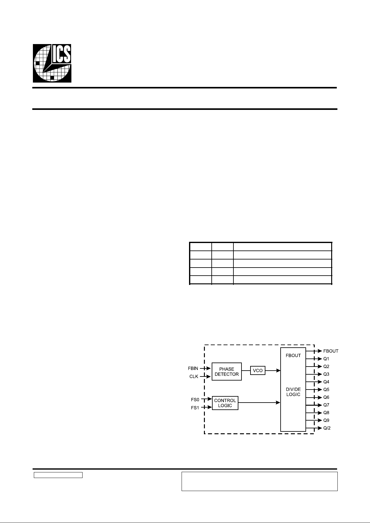
Block Diagram
ICS9176-01-01RevB061297P
Low Skew Output Buffer
Pentium is a trademark of Intel Corporation.
the ICS9176-01 is designed specifically to support the tight
timing requirements of high-performance microprocessors
and chip sets. Because the jitter of the device is limited to
±250ps, the ICS9176-01 is ideal for clocking Pentium™
systems. The 10 high drive (40mA), low-skew (±250ps)
outputs make the ICS9176-01 a perfect fit for PCI clocking
requirements.
The ICS9176-01 has 10 outputs synchronized in phase and
fre-quency to an input clock. The internal phase locked loop
(PLL) acts either as a 1X clock multiplier or a 1/2X clock
multiplier depending on the state of the input control pins T0
and T1. With metal mask options, any type of ratio between
the input clock and output clock can be achieved, including
2X.
The PLL maintains the phase and frequency relationship between the input clock and the outputs by externally feeding
back FBOUT to FBIN. Any change in the input will be tracked
by all 10 outputs. However, the change at the outputs will
happen smoothly so no glitches will be present on any driven
input. The PLL circuitry matches rising edges of the input
clock and the output clock. Since the input to FBIN skew is
guaran-teed to ±500ps, the part acts as a “zero delay” buffer.
The ICS9176-01 has a total of eleven outputs. Of these,
FBOUT is dedicated as the feedback into the PLL and another,
Q/2, has an output frequency half that of the remaining nine.
These nine outputs can either be running at the same speed as
the input, or at half the frequency of the input. With Q/2 as the
feedback to FBIN, the nine ‘Q’ outputs will be running at twice
the input frequency in the normal divide-by-1 mode. In this
case, the output can go to 120 MHz with a 60 MHz input clock.
The maximum rise and fall time of an output is 1ns and each is
TTL-compatible with a 40mA symmetric drive.
The ICS9176-01 is fabricated using CMOS technology which
results in much lower power consumption and cost compared
with the gallium arsenide based 1086E. The typical operating
current for the ICS9176-01 is 60mA versus 115mA for the
GA1086E.
Functionality
• ICS9176-01-01 is pin compatible with Triquint GA1086
• ±500ps skew (max) between input and outputs
• ±250ps skew (max) between outputs
• 10 symmetric, TLL-compatible outputs
• 28-pin PLCC or 28-pin wide SOIC surface mount
package
• High drive, 40mA outputs
• Power-down option
• Output frequency range 20 MHz to 120 MHz
• Input frequency range 20 MHz to 100 MHz
• Ideal for PCI bus applications
FS1 FS0 DESCRIPTION
0 0 Power-down
0 1 Test Mode (PLL Off CLK=outputs)
1 0 Normal (PLL On)
1 1 Divide by 2 Mode
ICS reserves the right to make changes in the device data identified in this publication
without further notice. ICS advises its customers to obtain the latest version of all
device data to verify that any information being relied upon by the customer is current
and accurate.
Page 2
2
ICS9176-01
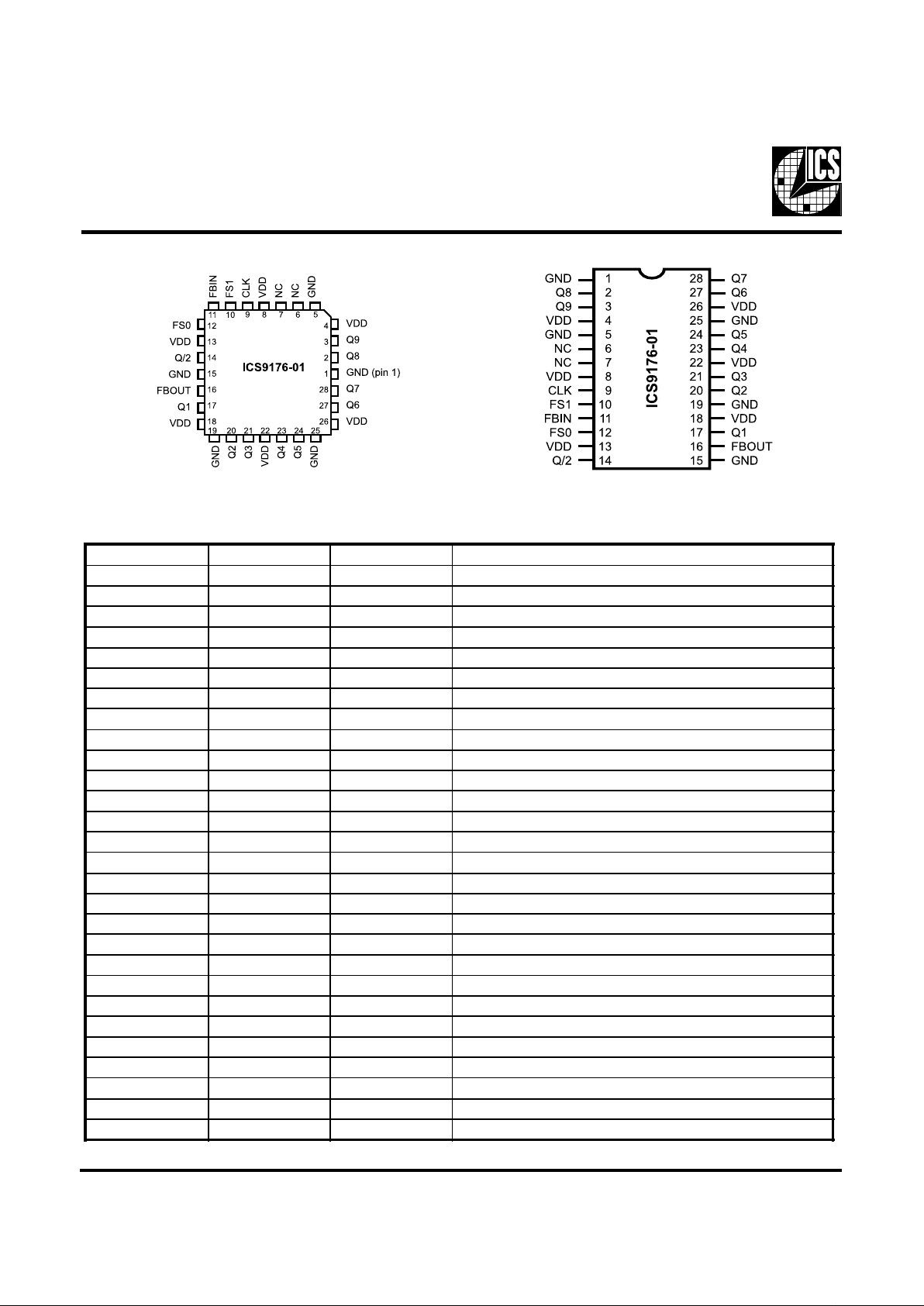
Pin Configuration
Pin Description
28-Pin PLCC
28-Pin SOIC
PIN NUMBER PIN NAME TYPE DESCRIPTION
1 GND - GROUND.
2 Q8 Output Output clock 8
3 Q9 Output Output clock 9.
4 VDD - Power supply (+5V).
5 GND - GROUND.
6 NC - No Connect.
7 NC - No Connect.
8 VDD - Power supply (+5V).
9 CLK Input Input for reference clock.
10 FS1 Input FS1 selects normal operation, power-down, or test mode.
11 FBIN Input FEEDBACK INPUT from output FBOUT.
12 FS0 Input FS0 selects normal operation, power-down, or test mode.
13 VDD - Power Supply (+5V).
14 Q/2 Output Half-clock output.
15 GND - GROUND.
16 FBOUT Output FEEDBACK OUTPUT to Input FBIN.
17 Q1 Output Output clock 1.
18 VDD - Power Supply (+5V).
19 GND - GROUND.
20 Q2 Output Output clock 2.
21 Q3 Output Output clock 3.
22 VDD - Power supply (+5V).
23 Q4 Output Output clock 4.
24 Q5 Output Output clock 5.
25 GND - GROUND.
26 VDD - Power Supply (+5V).
27 Q6 Output Output clock 6.
28 Q7 Output Output clock 7.
Page 3
3
ICS9176-01
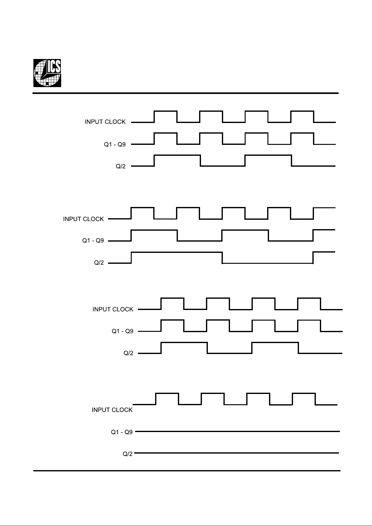
Timing Diagrams
Note: In test mode, the VCOs are bypassed. The test clock input is simply buffered, then output. The part is transparent. Damage
to the device may occur if an output is shorted or forced to ground or VDD.
Timing in Power-down Mode
Timing in Eliminate by Test Mode
Timing in Divide by 2 Mode
Timing in Divide by 1 Mode
Page 4

4
ICS9176-01
Absolute Maximum Ratings
VDD referenced to GND . . . . . . . . . . . . . . . . . . . . . . 7V
Operating temperature under bias. . . . . . . . . . . . . . . . 0°C to +70°C
Storage temperature . . . . . . . . . . . . . . . . . . . . . . . . . . -65°C to +150°C
Voltage on I/O pins referenced to GND. . . . . . . . . . . GND -0.5V to VDD +0.5V
Power dissipation . . . . . . . . . . . . . . . . . . . . . . . . . . . . 0.5 Watts
Stresses above those listed under Absolute Maximum Ratings may cause permanent damage to the device. This is a stress rating
only and functional operation of the device at these or any other conditions above those indicated in the operational sections
of the specifications is not implied. Exposure to absolute maximum rating conditions for extended periods may affect product
reliability.
Electrical Characteristics
DC Characteristics
VDD =+5V±5%, TA=0°C to 70°C unless otherwise stated
Note:
1. Guaranteed by design and characterization. Not subject to 100% test.
PARAMETER SYMBOL TEST CONDITIONS MIN TYP MAX UNITS
Input Low Voltage V
IL
VDD=5V - - 0.8 V
Input High Voltage V
IH
VDD=5V 2.0 - - V
Input Current I
i
VIN=0V, 5V -5 - 5 µ A
Output Low Voltage V
OL
@IOL=14mA - 0.25 0.4 V
Output Low Current I
OL
@VOL=0.8V 33 42 - mA
Output High Voltage
1
V
OH
@IOH=-38mA 2.4 - - V
Output High Current
1
I
OH
@VOH=2.0V - -59 -41 mA
Supply Current, Normal
Mode
I
DD
Unloaded outputs,
@ 66.6 Mhz
-5575mA
Supply Current, Powerdown Mode
I
DD-PD
T1, T0=0, 0 - 2.0 10.0 mA
Page 5

5
ICS9176-01
AC Characteristics
Notes:
1. Guaranteed by design and characterization. Not subject ot 100% test.
2. All skew specifications are measured with a 50W transmission line, load terminated with 50W to 1.4V.
3. Duty cycle measured at 1.4V.
4. Skew measured at 1.4V on rising edges. Loading must be equal on outputs.
PARAMETER SYMBOL TEST CONDITIONS MIN TYP MAX UNITS
Input Clock Pulse Width
1
CLK
W
VDD=4.5V, f
CLK
=100 MHz 2.5 - 7.5 ns
Output Rise time, 0.8 to
2.0V
1
t
r
15pF load - 0.7 1 ns
Rise time, 20% to 80%
V
DD
1
t
r
15pF load - 1.5 2 ns
Output Fall time, 2.0V to
0.8V
1
t
f
15pF load - 0.7 1 ns
Fall time, 80% to 20%
V
DD
1
t
f
15pF load - 1.2 2 ns
Output Duty cycle
1
d
t
15pF load, Note 3 45 49/51 55 %
Jitter, 1 sigma
1
T
ls
-60-ps
Jitter, absolute
1
T
abs
-250 ±100 250 ps
Input Frequency f
i
20 - 100 MHz
Output Frequency
(Q outputs)
f
o
For outputs >100 MHz, use
Q/2 as feedback
20 - 120 MHz
FBIN to IN skew
1
t
skew1
Note 2, 4. Input rise time <
3ns
-500 250 0 ps
Skew between any 2 outputs at same frequency
1
t
skew2
Note 2, 4. -250 50 250 ps
Skew between any 1 out
put and Q/2
1
t
skew3
Note 2, 4 -3 ±0.1 3 ns
Page 6

6
ICS9176-01
Applications
FBOUT is normally connected to FBIN to facilitate input to
output skew control. However, there is no requirement that
the external feedback connection be a direct hardwire from an
output pin to the FBIN pin. As long as the signal at FBIN is
derived directly from the FBOUT pin and maintains its frequency, additional delays can be accommodated. The clock
phase of the outputs (rising edge) will be adjusted so that the
phase of FBIN and the input clock will be the same. See Figure
1 for an example.
Figure 1
In Figure 1, the propagation delay through the divide by 2
circuit is eliminated. The internal phase-locked loop will
adjust the output clock on the ICS9176-01 to ensure zero
phase delay between the FBIN and CLK signals, as a result,
the rising edge at the output of the divide by two circuit will be
aligned with the rising edge of the 66 MHz input clock. This
type of configuration can be used to eliminate propagation
delay as long as the signal at FBIN is continuous and is not
gated or conditional.
Figure 2
The ICS9176-01 is also ideal for clocking multi-processor
sys-tems. The 10 outputs can be used to synchronize the
operation of CPU cache and memory banks operating at
different speeds. Figure 2 depicts a 2-CPU system in which
processors and associated peripherals are operating at 66
MHz. Each of the nine outputs operating at 66 MHz are fully
utilized to drive the appropriate CPU, cache and memory control
logic. The 33 MHz output is used to synchronize the operation
of the slower memory bank to the restart of the system.
Page 7

7
ICS9176-01
ICS XXXX- M PPP
Pattern Number (2 or 3 digit number for parts with ROM code patterns)
Package Type
Q=PLCC
Device Type (consists of 3 or 4 digit numbers)
Prefix
ICS, A V=Standard Device
Ordering Information
ICS9176Q-01
Example:
PLCC P ackage
LEAD COUNT
FRAME
THICKNESS
T
F
±.0003
PKG.
THICKNESS
T
P
±.004
PKG. WIDTH
TOP
W
T
±.004
PKG. WIDTH
BOTTOM
W
B
±.006
OVERALL
PKG. WIDTH
W
O
±.005
CONTACT
WIDTH
W
O
+.010/-.030
28L 0.010 0. 152 0.450 0.453 0.490 0. 420
Page 8

8
ICS9176-01
Ordering Information
ICS9176M-01
Example:
SOIC Packag e
ICS XXXX- M PPP
Pattern Number (2 or 3 digit number for parts with ROM code patterns)
Package Type
M=SOIC
Device Type (consists of 3 or 4 digit numbers)
Prefix
ICS, A V=Standard Device
LEAD COUNT 28L
DIMENSION L 0.704
ICS reserves the right to make changes in the device data identified in this publication
without further notice. ICS advises its customers to obtain the latest version of all
device data to verify that any information being relied upon by the customer is current
and accurate.
 Loading...