

Datasheet AV9172-07CW16, AV9172-07CS16, AV9172-07CN16, AV9172-03CW16, AV9172-03CS16 Datasheet (ICST)
...Page 1
Integrated
Circuit
Systems, Inc.
General Description Features
AV 91 7 2
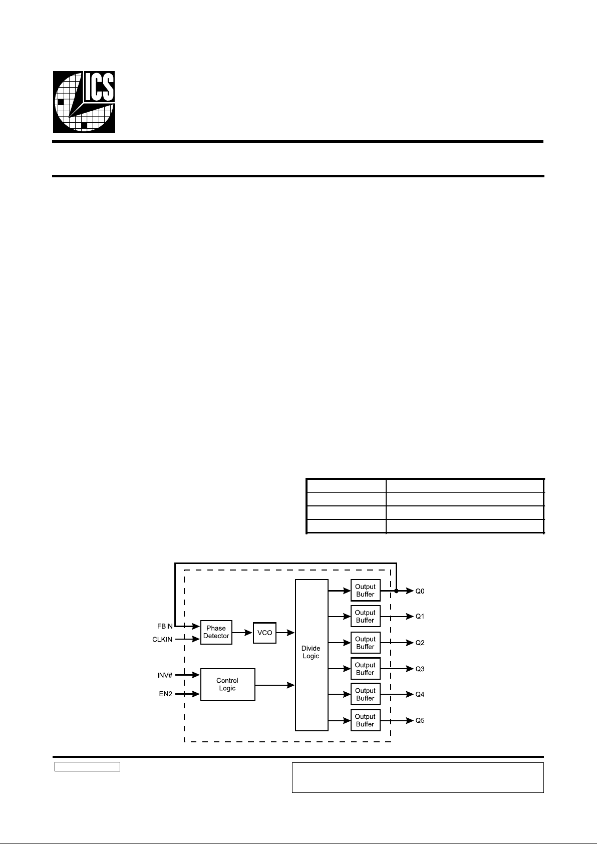
Block Diagram
AV9172RevB060297P
The A V9172 is designed to generate low skew clocks for
clock distribution in high-performance PCs and workstations.
It uses phase-locked loop technology to align the phase and
frequency of the output clocks with an input reference clock.
Because the input to output skew is guaranteed to ± 500ps, the
part acts as a “zero delay” buffer.
The AV9172 has six configurable outputs. The AV9172-01
version has one output that runs at the same phase and
frequency as the reference clock. A second output runs at the
same frequency as the reference, but can either be in phase or
180° out of phase from the input clock. Two outputs are
provided that are at twice the reference frequency and in
phase with the reference clock. The final outputs can be
programmed to be replicas of the 2x clocks or non-overlapping
two phase clocks at twice the reference frequency. The
AV9172-01 and AV9172-03 operates with input clocks
from 10 MHz to 50 MHz while producing outputs from
10 MHz to 100 MHz. The AV9172-07 operates with input
clocks from 20 to 100 MHz.
The use of a phase-locked loop (PLL) allows the output
clocks to run at multiples of the input clock. This permits
routing of a lower speed clock and local generation of a
required high speed clock. Synchronization of the phase
relationship between the input clock and the output clocks is
accomplished when one output clock is connected to the
input pin FBIN. The PLL circuitry matches rising edges of the
input clock and output clocks.
• AV9172-07 input is 66 MHz with 66 and 33 MHz
output buffers
• AV9172-01 is pin compatible with Gazelle GA1210E
• ±250ps skew (max) between outputs
• ±500ps skew (max) between input and outputs
• Input frequency range from 10 MHz to 50 MHz
(-01, -03) and from 20 MHz to 100 MHz (-07)
• Output frequency range from 10 MHz to 100 MHz
(-01, -03, -07)
• Special mode for two-phase clock generation
• Inputs and outputs are fully TTL-compatible
• CMOS process results in low power supply current
• High drive, 25mA outputs
• Low cost
• 16-pin SOIC (150-mil) or 16-pin PDIP package
Low Skew Output Buffer
The AV9172 is fabricated using CMOS technology which
results in much lower power consumption and cost compared
with the gallium arsenide-based GA1210E. The typical
operating current for the AV9172 is 50mA versus 120mA for
the GA1210E.
ICS offers several versions of the AV9172. The different
devices are shown below:
PART DESCRIPTION
AV9172-01 Second source of GA1210E
AV9172-03 Clock doubler and buffer
AV9172-07 Clock buffer for 66 MHz input
ICS reserves the right to make changes in the device data identified in this publication
without further notice. ICS advises its customers to obtain the latest version of all
device data to verify that any information being relied upon by the customer is current
and accurate.
Page 2
2
AV9172
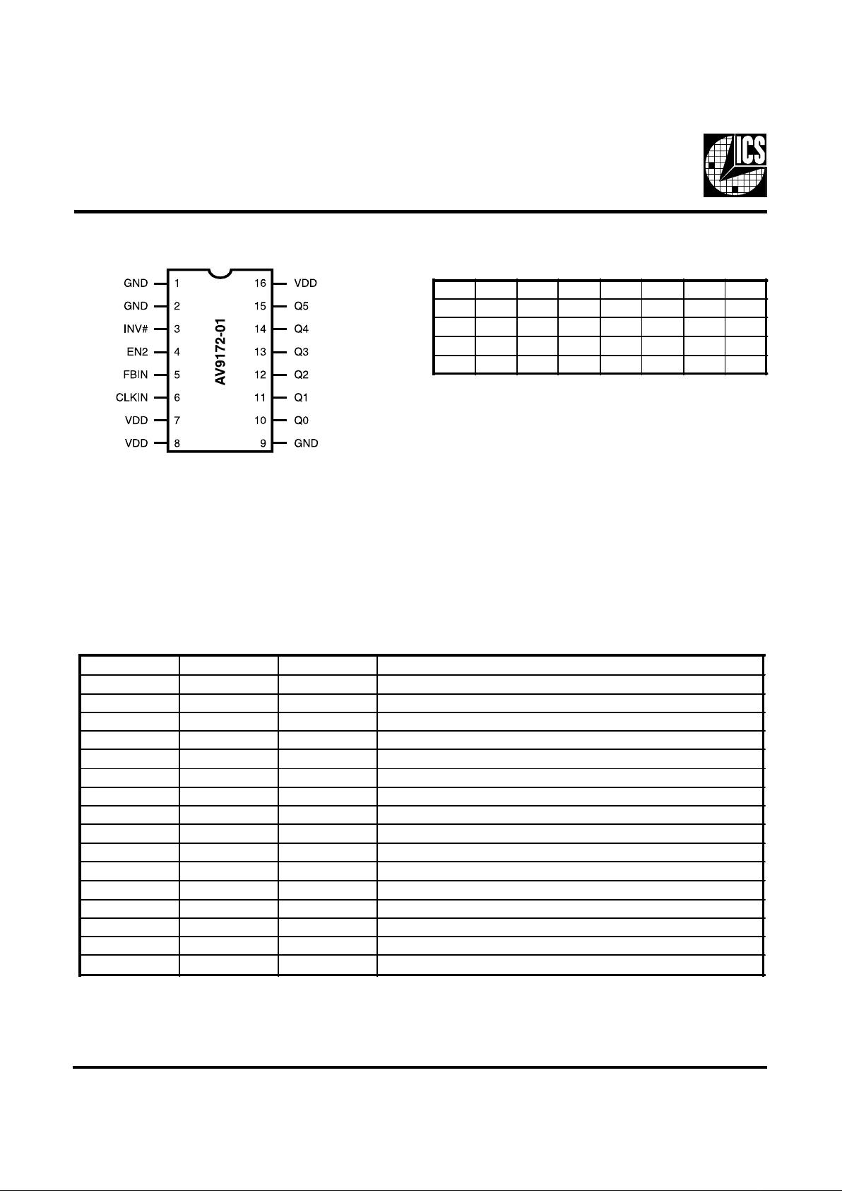
Pin Configuration
Pin Description f or AV9172-01
16-Pin SOIC or 16-Pin PDIP
Functionality Table for AV9172-01
CLKIN input frequency range 10 to 50 MHz.
Notes:
1. 1X designates that the output is a replica of CLKIN.
2. 2X designates that the output is twice the frequency of
CLKIN, and in phase.
3. 1X# means that the output is at the same frequency and
180°C out of phase (inverted) from CLKIN.
4. Ø1 will produce a ¼ duty cycle clock of CLKIN.
5. Ø2 will produce a ¼ duty cycle clock delayed 180° from
CLKIN.
EN2 INV# Q0 Q1 Q2 Q3 Q4 Q5
0 0 1X 1X# 2X 2X 2X 2X
0 1 1X 1X 2X 2X 2X 2X
1 0 1X 1X# 2X 2X
∅1 ∅2
1 1 1X 1X 2X 2X
∅1 ∅2
PIN NUMBER PIN NAME TYPE DESCRIPTION
1 GND - GROUND.
2 GND - GROUND.
3 INV# Input INV# Inverts Q1 when low. (-01 [divisor select -03, -07])
4 EN Input EN converts Q4 and Q5 to phase clocks when high.
5 FBIN Input FEEDBACK INPUT from output Q0.
6 CLKIN Input INPUT for reference clock.
7 VDD - Power supply (+5V).
8 VDD - Power supply (+5V).
9 GND - GROUND.
10 Q0 Output Q0 phase and frequency same as input (1X). Feed back to pin 5.
11 Q1 Output Q1 is a 1x clock in phase or 180° out of phase with input.
12 Q2 Output Q2 twice the frequency of Q0 (2x).
13 Q3 Output Q3 twice the frequency of Q0 (2x).
14 Q4 Output Q4 is either a 2X clock or a two-phase clock - see configuration table.
15 Q5 Output Q5 is either a 2X clock or a two-phase clock - see configuration table.
16 VDD - Power supply (+5V).
Page 3
3
AV9172
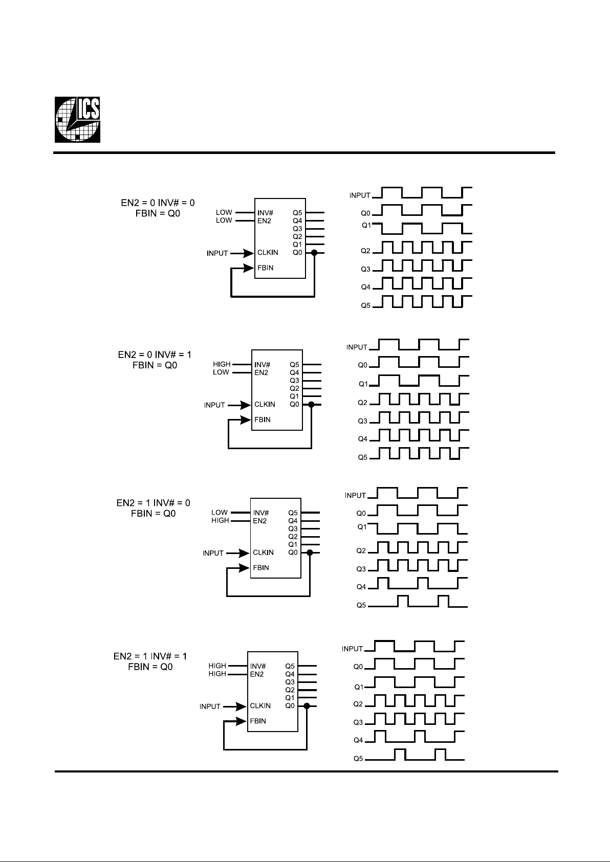
Timing Diagrams for AV9172-01
Page 4

4
AV9172
Pin Configuration
Functionality Table for AV9172-03
CLKIN Input Frequency=X, input range is 10 to 50 MHz.
Example T able for A V9172-03
(33 MHz input, all frequencies in MHz.)
Timing Diagram f or AV9172-03
16-Pin SOIC or 16-Pin PDIP
Note: The phase alignment between the 1X clock outputs and
reference clocks input will be either at a 0 or 180 degrees
offset if the 2X clock is used as the feedback signal (connected to the FBIN pin). Which relationship occurs is totally
random and has the potential to change any time the device has
its VDD supply cycled off or the devices input clock
removed.
EN2 INV# Q0 Q1 Q2 Q3 Q4 Q5
0 0 2X 2X 2X 2X 2X 2X
1 0 2X 2X 2X 2X 2X 1X
0 1 2X 2X 2X 1X 1X 2X
1 1 2X 2X 2X 1X 1X 1X
EN2 INV# Q0 Q1 Q2 Q3 Q4 Q5
0 0 66 66 66 66 66 66
1 0 66 66 66 66 66 33
0 1 66 66 66 33 33 66
1 1 66 66 66 33 33 33
Page 5

5
AV9172
Absolute Maximum Ratings
VDD referenced to GND . . . . . . . . . . . . . . . . . . . . . . 7V
Operating temperature under bias. . . . . . . . . . . . . . . . 0°C to +70°C
Storage temperature . . . . . . . . . . . . . . . . . . . . . . . . . . -65°C to +150°C
Voltage on I/O pins referenced to GND. . . . . . . . . . . GND -0.5V to VDD +0.5V
Power dissipation . . . . . . . . . . . . . . . . . . . . . . . . . . . . 0.5 Watts
Stresses above those listed under Absolute Maximum Ratings may cause permanent damage to the device. This is a stress rating
only and functional operation of the device at these or any other conditions above those indicated in the operational sections
of the specifications is not implied. Exposure to absolute maximum rating conditions for extended periods may affect product
reliability.
Pin Configuration Functionality Table for AV9172-07
CLKIN Input Frequency=X, input range is 20 to 100 MHz.
Example Table for AV9172-07
(66 MHz input, all frequencies in MHz.)
16-Pin SOIC or 16-Pin PDIP
Timing Diagram f or AV9172-07
EN2 INV# Q0 Q1 Q2 Q3 Q4 Q5
0 0 1X 1X 1X 1X 1X 1X
1 0 1X 1X 1X 1X 1X 0. 5X
0 1 1X 1X 1X 0.5X 0.5X 1X
1 1 1X 1X 1X 0.5X 0.5X 0.5X
EN2 INV# Q0 Q1 Q2 Q3 Q4 Q5
0 0 66 66 66 66 66 66
1 0 66 66 66 66 66 33
0 1 66 66 66 33 33 66
1 1 66 66 66 33 33 33
Page 6

6
AV9172
Electrical Characteristics
VDD =+5V±5%, TA=0°C to 70°C unless otherwise stated
*Parameter guaranteed by design and characterization. Not 100% tested in production.
Notes:
1. Output frequency includes both the Fast Clock (2X or 1X) and the Slow Clock (1X or 0.5X) extremes.
2. All skew specifications are measured with a 50W transmission line, load terminated with 50W to 1.4V.
3. Duty cycle measured at 1.4V.
4. Skew measured at 1.4V on rising edges. Loading must be equal on outputs.
DC Characteristics
PARAMETER SYMBOL TEST CONDITIONS MIN TYP MAX UNITS
Input Low Voltage V
IL
VDD=5V - - 0.8 V
Input High Voltage V
IH
VDD=5V 2.0 - - V
Input Low Current I
IL
VIN=0V -5 - 5 µA
Input High Current I
IH
VIN=V -5 - 5 µA
Output Low Voltage VOL*IOL=25mA - 0.5 0.8 V
Output High Voltage VOH*IOH=-25mA 2.4 - - V
Supply Current I
DD
Unloaded, 50 MHz outputs - 35 60 mA
AC Characteristics
Input Clock Rise Time ICLKr*--10ns
Input Clock Fall Time ICLKf*--10ns
Output Rise time, 0.8 to 2.0V tr* 15pF load - 0.7 1 ns
Rise time, 20% to 80% V
DD
tr* 15pF load - 1.2 2 ns
Output Fall time, 2.0 to 0.8V tf* 15pF load - 0.7 1 ns
Fall time, 80% to 20% V
DD
tf* 15pF load - 1.2 2 ns
Output Duty cycle dt* 15pF load 45 49/51 55 %
Jitter, 1 sigma T
1s
*60ps
Jitter, absolute T
abs
* ae200 ps
Input Frequency (-01,-03) fi* 10 50 MHz
Input Frequency (-07) fi* 20 100 MHz
Output Frequency
(-01,-03, -07)
f
o
* Note 1 10 100 MHz
FBIN to IN skew t
skew1
*
Note 2, 4. Input rise time
< 3ns
-500 -300 500 ps
FBIN to IN skew t
skew1
*
Note 2, 4. Input rise time
< 10ns
1000 -500 1000 ps
Skew between any 2 outputs at
same frequency
t
skew2
*
Note 2, 4 -250 ±50 250 ps
Skew between any 2 outputs at
different frequencies
Note 2, 4 500 ps
Page 7

7
AV9172
T ypical Performance Characteristics
Page 8

8
AV9172
Ordering Information
ICS XXXX-PPP M X#W
Pattern Number (2 or 3 digit number for parts with ROM code patterns)
Device Type (consists of 3 or 4 digit numbers)
Prefix
ICS, A V=Standard Device
Example:
16-Pin PDIP P ackage
16-Pin SOIC P ac kage
Part Number Part Marking Temperature Package Type
AV9172-xxCC16 AV9172-XX 0°C to 70°C 16 Lead CERDIP
AV9172-xxCN16 AV9172-XX 0°C to 70°C 16 Lead Plastic DIP (300 mil)
AV9172-xxCW16 AV9172-XX 0°C to 70°C 16 Lead SOIC (300 mil)
AV9172-xxCS16 AV9172-XX 0°C to 70°C 16 Lead SOIC (150 mil)
Lead Count & Package Width
Lead Count=1, 2 or 3 digits
W=.3” SOIC or .6” DIP; None=Standard Width
Package Type
C=CERDIP N=DIP (Plastic#)
W=SOIC (300 mil) S=SOIC (150 mil)
ICS reserves the right to make changes in the device data identified in this publication
without further notice. ICS advises its customers to obtain the latest version of all
device data to verify that any information being relied upon by the customer is current
and accurate.
 Loading...