

Page 1
Integrated
Circuit
Systems, Inc.
Low Cost 20-Pin Frequency Generator
ICS9169C-36
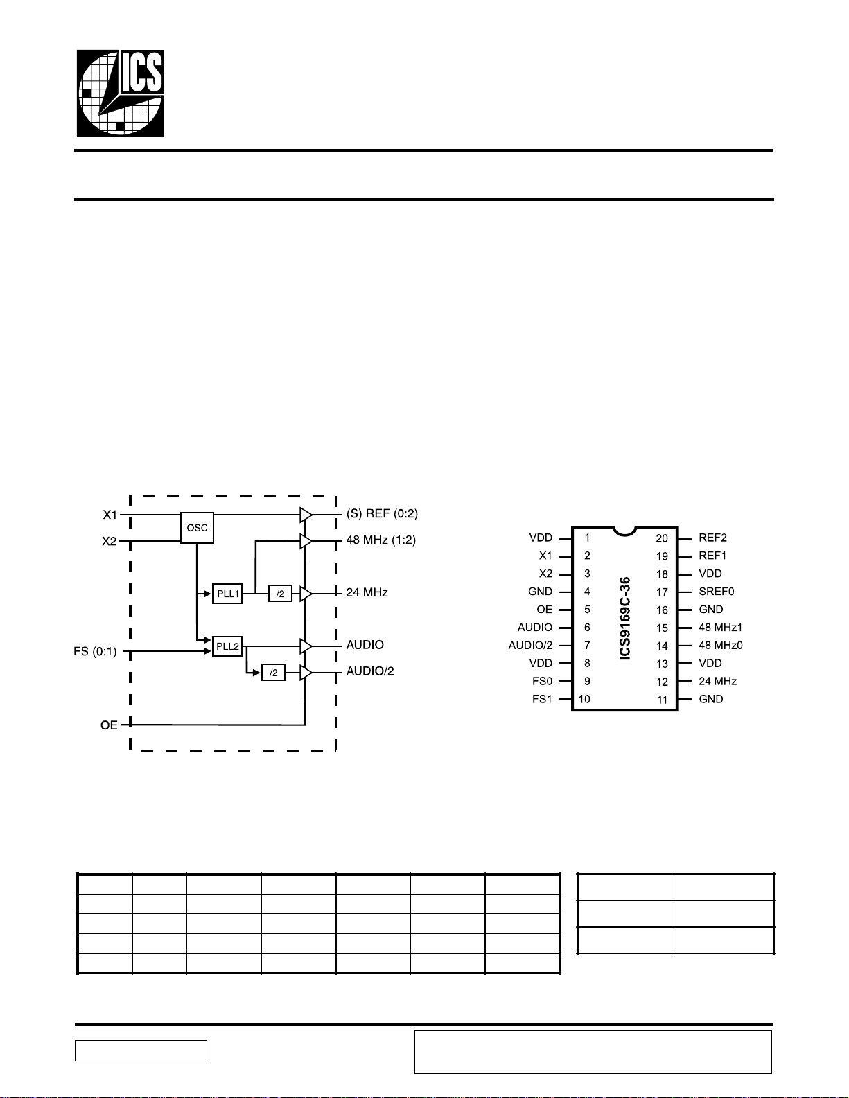
Description
The ICS9169C-36 generates the I/O clocks needed as a satellite
clock generator to a CPU and PCI clock source (such as the
ICS9148-01 or ICS9150-01). This device can generate the
audio Codec or DSP clocks if required (or Stop those outputs
Low).
The device is nominally driven at the X1 pin by a 14.31818
MHz clock source. The device can also be driven by a crystal
using external load capacitors as a stand-alone generator.
The SREF0 output is a reference clock output which is stronger
to allow multiple ISA slots.
Block Diagram
Features
• Generator for periphary clock chips as companion
device to CPU/SDRAM/PCI generator .
• Accepts clock input at X1 pin or crystal across X1,
X2 pins as 14.31818 MHz nominal inputs.
• Three REF clock buffer outputs (SREF is Strong)
• Two 48MHz and one 24 MHz outputs
• Selectable audio clock generator with audio (Audio)
and half speed (Audio/2) outputs
• 20 pin (209 mil) SSOP package
Pin Configuration
Functionality
3.3V±10%, 0-70°C
Clock source driving X1 pin or crystal (X1, X2) = 14.31818 MHz
(all frequencies in MHz)
FS1 FS0 AUDIO AUDIO/2 SREF, REF 48 MHz 24 MHz
0 0 XTAL/2 XTAL/4 14.318 XTAL/2 XTAL/4
0 1 24. 5795 12.2898 14.318 48.008 24. 004
1 0 33. 8680 16.9340 14.318 48.008 24. 004
1 1 LOW LOW 14.318 48.008 24. 004
ICS reserves the right to make changes in the device data identified in this publication
ICS9169C-36RevD060197P
without further notice. ICS advises its customers to obtain the latest version of all
device data to verify that any information being relied upon by the customer is current
and accurate.
20-Pin SSOP
OE All Outputs
0 Tristate
1 Active
Page 2
ICS9169C-36
Pin Descriptions
PIN NUMBER PIN NAME TYPE DESCRIPTION
1, 8, 13, 18 VDD PWR 3.3V I/O power supply
2X1IN
3 X2 OUT Crystal output (no connect for non-crystal applications)
4, 11, 16 GND Ground Ground
5 OE IN Output enable (Tri-states all outputs when held low). Has pullup
6 AUDIO OUT 3.3V Audio clock, runs per select table
7 AUDIO/2 OUT 3.3V Audio clock, runs per select table
9, 10 FS0, FS1 IN Frequency mode select pins. Has pullup.
12 24 MHz OUT 3.3V clock, runs @ 24 MHz
14, 15 48 MHz (0:1) OUT 3.3V Clock, runs @ 48 MHz
19, 20
17 SREF0 OUT Strong reference clock OUT 3.3V clock, runs @ 1x X1
REF1, REF2
(1:2)
14.318MHz input (requires external components for feedback
resistor and load capacitors to be used with a crystal)
OUT 3.3V clock, runs @ 1x X1
2
Page 3

ICS9169C-36
Absolute Maximum Ratings
Supply Voltage ............................................................................................................ 7.0 V
Voltage on I/O pins referenced to GND ............................... GND –0.5 V to VDD +0.5 V
Operating Temper ature under bias ..............................................................0°C to +70°C
Power dissipation................................................................................................. 0.5 Watts
Storage Temperature .............................................................................. –40°C to +150°C
Stresses above those listed under Absolute Maximum Ratings may cause permanent damage to the device. These ratings are
stress specifications only and functional operation of the device at these or any other conditions above those listed in the
operational sections of the specifications is not implied. Exposure to absolute maximum rating conditions for extended
periods may affect product reliability.
Electrical Characteristics at 3.3V
VDD = 3.0 – 3.7 V, TA = 0 – 70°C unless otherwise stated
DC Characteristics
PARAMETER SYMBOL TEST CONDITIONS MIN TYP MAX UNITS
Input Low Voltage V
Input High Voltage V
Input Low Current I
Input High Current I
Output Low Voltage V
Output High Voltage V
Output Low Current I
Output High Current I
Output Low Voltage V
Output High Voltage V
Output Low Current I
Output High Current I
Output Low Voltage V
Output High Voltage V
Output Low Current I
Output High Current I
Supply Current I
Output Frequency Change
over Supply and Temperature
Short circuit current
Input Capacitance
Load Capacitance
1
1
1
1
Pull-up Resistor R
OL1
OH1
OL2
OH2
OL3
OH3
F
I
C
C
IL
IH
IL
IH
OL1
OH1
OL2
OH2
OL3
OH3
DD
D
SC
pu
VDD=3.3V - - 0.2V
VDD=3.3V 0.7V
DD
--V
DD
V
VIN=0V (pull-up pin) -250 -50 µ A
VIN=V
DD
-5 0 5 µA
SREF0 IOL = 16mA 0.25 0.40 V
SREF0 IOH = -16mA 2.4 2.8 V
SREF0 VOL = 1.0V 32 50 mA
SREF0 VOH = 2.0V -44 -28 mA
AUDIO, AUDI O/2,
24MHz, 48M Hz (0:1) Clocks
I
= 10mA
OL
0.25 0.4 V
AUDIO, AUDI O/2,
24MHz, 48M Hz (0:1) Clocks
I
= -10mA
OH
2.4 2.8 V
AUDIO, AUDI O/2,
24MHz, 48M Hz (0:1) Clocks
V
= 0.8V
OL
19 30 mA
AUDIO, AUDI O/2,
24MHz, 48M Hz (0:1) Clocks
V
= 2.0V
OH
-26 -16 mA
REF (1:2) IOL = 8mA 0.3 0.4 V
REF (1:2) IOH = -8mA 2.4 2.8 V
REF (1:2) V
REF (1:2) V
= 0.8V 16 25 mA
OL
= 2.0V -22 -14 mA
OH
Unloaded, 33.86 MHz - 28 45 mA
With respect to typical
frequency
- 20 100 ppm
Each output clock 20 30 - mA
Except X1, X2 - - 10 pF
I
Pins X1, X2 - 5 - pF
L
at VIN=VDD-1V 15 30 60 k ohm
Note 1: Parameter is guaranteed by design and characterization. Not 100% tested in production.
3
Page 4

ICS9169C-36
Electrical Characteristics at 3.3V
VDD = +3.0 V±10%, TA = 0 – 70°C unless otherwise stated
AC Characteristics
PARAMETER SYMBOL TEST CONDITIONS MIN TYP MAX UNITS
Input Clock Rise Time
Input Clock Fall Time
Rise time
1
SREF0 output t
Slew SREF0 Rising
Fall time
1
SREF0 output t
Slew SREF0 Falling
Rise time
Fall time
Duty cycle
1
other outputs t
1
other outputs t
1
Jitter, one sigma
Jitter, absolute
Jitter, absolute
Jitter, absolute
1,2
1,2
1,2
Input Frequency
Normal output frequency F
Ratio of Nominal frequency
to target frequency
Clock skew between
AUDIO/2 and
AUDIO outputs
Power-up Time
1
1
1
1
1,2
1
t
ICr
t
ICf
r1
S
lew1
f1
S
lew2
r2
f2
d
t
jls 1
t
jab1
t
jab2
t
jab3
f
in
45pF load, 0.8 to 2.0V 0.3 1.3 2.0 ns
45pF 0.4 to 2.4V 0.8 0.95 4.0 V/ns
45pF load, 0.8 to 2.0V 0.3 1.0 2.0 ns
45pF 2.4 to 0.4V 0.8 0.95 4.0 V/ns
20pF load, 0.8 to 2.0V 0.6 1.2 2.0 ns
20pF load, 0.8 to 2.0V 0.6 0.9 2.0 ns
25pF load at 1.5V (All outputs) 45 50 55 %
t
10,000 cycles (All outputs) - 100 250 ps
10,000 cycles 24, Audio, Audio/2 750 - 750 ps
10,000 cycles 48MHz -500 500 ps
10,000 cycles REF CLKS -3.5% - 3.5 %
with X1 driven at 14.31818MHz
NOM
with X1 driven at 14.31818MHz
1
1
1
f/f
T
sk
t
tPO
to 33.8 MHz on Audio - 5 10 ms
48MHz
24MHz
33.86MHz
24.5795MHz
24.0MHz
48.0MHz
33.8688MHz
24.576MHz
- - 20 ns
- - 20 ns
11 14.318 16 MHz
48.008MHz
24.004MHz
MHz
33.8650MHz
24.5795MHz
166
166
-200
-200
166.6
166.6
-23.6
+144
167
167
+200
+200
ppm
250 - +250 ps
Note 1: Parameter is guaranteed by design and characterization. Not 100% tested in production.
Note 2: Absolute Jitter is defined as largest difference of the shortest period to the mean or the longest period to the
mean in a sampling of 10,000 clock cycles. One Sigma Jitter is the calculated standard deviation.
4
Page 5

ICS9169C-36
209 mil 20Pin SSOP Package
COMMON
SYMBOL
MIN. NOM. MAX. N MIN. NOM. MAX.
A 0.068 0.073 0.078 14 0.239 0.244 0.249
A1 0.002 0.005 0.008 16 0.239 0.244 0.249
A2 0.066 0.068 0.070 20 0.278 0.284 0.289
b 0.010 0.012 0.015 24 0.318 0.323 0.328
c 0.004 0.006 0.008 28 0.397 0.402 0.407
D See Variations 30 0.397 0.402 0.407
E 0.205 0.209 0.212
e 0.0256 BSC
H 0.301 0.307 0.311
L 0.025 0.030 0.037
N See Variations
∝
0° 4° 8°
DIMENSIONS
VARIATIONS
Dimensions in inches
D
Ordering Information
ICS9169CF-36
Example:
ICS XXXX F-PPP
Pattern Number(2 or 3 digit number for parts with ROM code patterns)
Package Type
F=SSOP
Device Type (consists of 3 or 4 digit numbers)
Prefix
ICS=Standard Device
ICS reserves the right to make changes in the device data identified in this publication
without further notice. ICS advises its customers to obtain the latest version of all
5
device data to verify that any information being relied upon by the customer is current
and accurate.
 Loading...