

Page 1
Integrated
Circuit
ICS9169C-231
Systems, Inc.
Frequency Generator for Pentium™ Based Systems
General Description Features
The ICS9169C-231 is a low-cost frequency generator
designed specifically for Pentium and Pentium-Pro based
chip set systems. The integrated buffer minimizes skew
and provides all the clocks required. A 14.318 MHz XTAL
oscillator provides the reference clock to generate standard
Pentium frequencies. The CPU clock makes gradual
frequency transitions without violating the PLL timing of
internal microprocessor clock multipliers. A raised
frequency setting of 68.5 MHz is available for Turbo-mode
of the 66.8 MHz CPU. The ICS9169C-231 contains 8 CPU
clocks, 6 PCI clocks, 1 REF at 48MHz and 1 at 24MHz.
Either synchronous (CPU/2) or asynchronous (32 MHz)
PCI bus operation can be selected by latching data on
BSEL input.
• Eight selectable CPU clocks operate up to 83.3 MHz
• Frequency selections include Turbo-mode speed of
68.5 MHz
• Maximum CPU jitter of ±200ps
• Six BUS clocks support sync or async bus operation
• 250ps skew window for CPU outputs, 500ps skew
window for BUS outputs
• CPU clocks to BUS clocks skew 1-4 ns (CPU early)
• 48 MHz clock for USB support & 24 MHz clock for FD.
• Logic inputs latched at Power-On for frequency
selection saving pins as Input/Output
• Integrated buffer outputs drive up to 30pF loads
• 3.0V - 3.7V supply range, CPU (1:8) outputs 2.5V
(2.375 - 2.6V) VDD option
• 28-pin SOIC or SSOP package
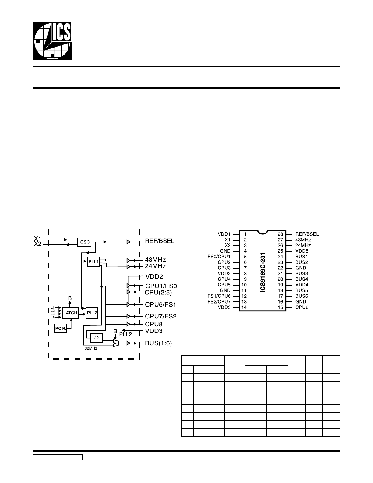
Block Diagram
VDD Groups:
VDD1 = X1, X2, REF/BSEL
VDD2 = CPU1-6
VDD3 = CPU7-8 & PLL Core
VDD4 = BUS1-6
VDD5 = 48/24 MHz
Latched Inputs:
L1 = BSEL
L2 = FS0
L3 = FS1
L4 = FS2
Pin Configuration
28-Pin SOIC or SSOP
Functionality
3.3V±10%, 0-70°C
Crystal (X1, X2) = 14.31818 MHz
ADDRESS
SELECT
FS2 FS1 FS0 BSEL=1 BSEL=0
0005025324824REF
0016030324824REF
0 1 0 66. 8 33. 4 32 4 8 24 RE F
01 1 75.9 32 32 48 24REF
10 0 55 27.5 32 48 24REF
1 0 1 75. 9 37. 5 32 4 8 24 RE F
1 1 0 83. 3 41. 7 32 4 8 24 RE F
1 1 1 68.5 34.25 32 48 24 REF
CPU(1:8)
(MHz)
BUS (1:6)MHz
48MHz 24MHz REF
Pentium is a trademark of Intel Corporation.
9169C-231RevB040697P
ICS reserves the right to make changes in the device data identified in this publication
without further notice. ICS advises its customers to obtain the latest version of all
device data to verify that any information being relied upon by the customer is current
and accurate.
Page 2
ICS169C-231
Pin Descriptions
PIN NUMBER PIN NAME TYPE DESCRIPTION
1 VDD1 PWR
2X1 IN
3 X2 OUT
4,11,16,22 GND PWR Ground for control logic.
6,7,9,10,15 CPU(2,3,4,5,8) OUT
5,12,13
5,12,13 FS (0:2) IN
8 VDD2 PWR
14 VDD3 PWR
17,18,20,21,23, 24 BUS(1:6) OUT
19 VDD4 PWR Power for BUS clock buffers BUS (1:6)
25 VDD5 PWR Power for fixed clock buffer (48 MHz, 24 MHz)
26 24 MHz OUT Fixed 24 MHz clock (assuming a 14.31818 MHz REF frequency).
27 48 MHz OUT Fixed 48 MHz clock (assuming a 14.31818 MHz REF frequency).
28
CPU1, CPU6,
CPU7
REF OUT Fixed 14.31818 MHz clock (assuming a 14.31818 MHz REF frequency).
BSEL IN
OUT
Power for control logic and crystal oscillator circuit and
14.318 MHz output
XTAL or external reference frequency input. This input includes XTAL
load capacitance and feedback bias for a 12-16MHz crystal, nominally
14.31818mhz. External crystal load of 30pF to GND recommended for
VDD power on faster than 2.0ms.
XTAL output drive from device. XTAL output which includes XTAL load
capacitance. External crystal load of 10pF to GND recommended for VDD
power on faster than 2.0ms.
Processor clock outputs which are a multiple of the input reference clock
as shown in the preceding table.
Processor clock outputs which are a multiple of the input reference clock
as shown in the preceding table.
Frequency multiplier select pins. See shared pin programming description
later in this data sheet for further explanation. 350K* internal pull up.
Power for CPU (1:6) clock buffers only. This VDD supply can be reduced
to 2.5V for CPU (1:6) outputs.
Power for CPU (7:8) clock buffers and internal PLL and Core logic. Must
be nominal 3.3V (3.0 to 3.7V)
BUS clock outputs which are a multiple of the input reference clock as
shown in the preceding table.
Selection for synchronous or asynchronous bus clock operation. 350K*
internal pull up.
* The internal pull up will vary from 350K to 500K based on temperature
2
Page 3
ICS169C-231
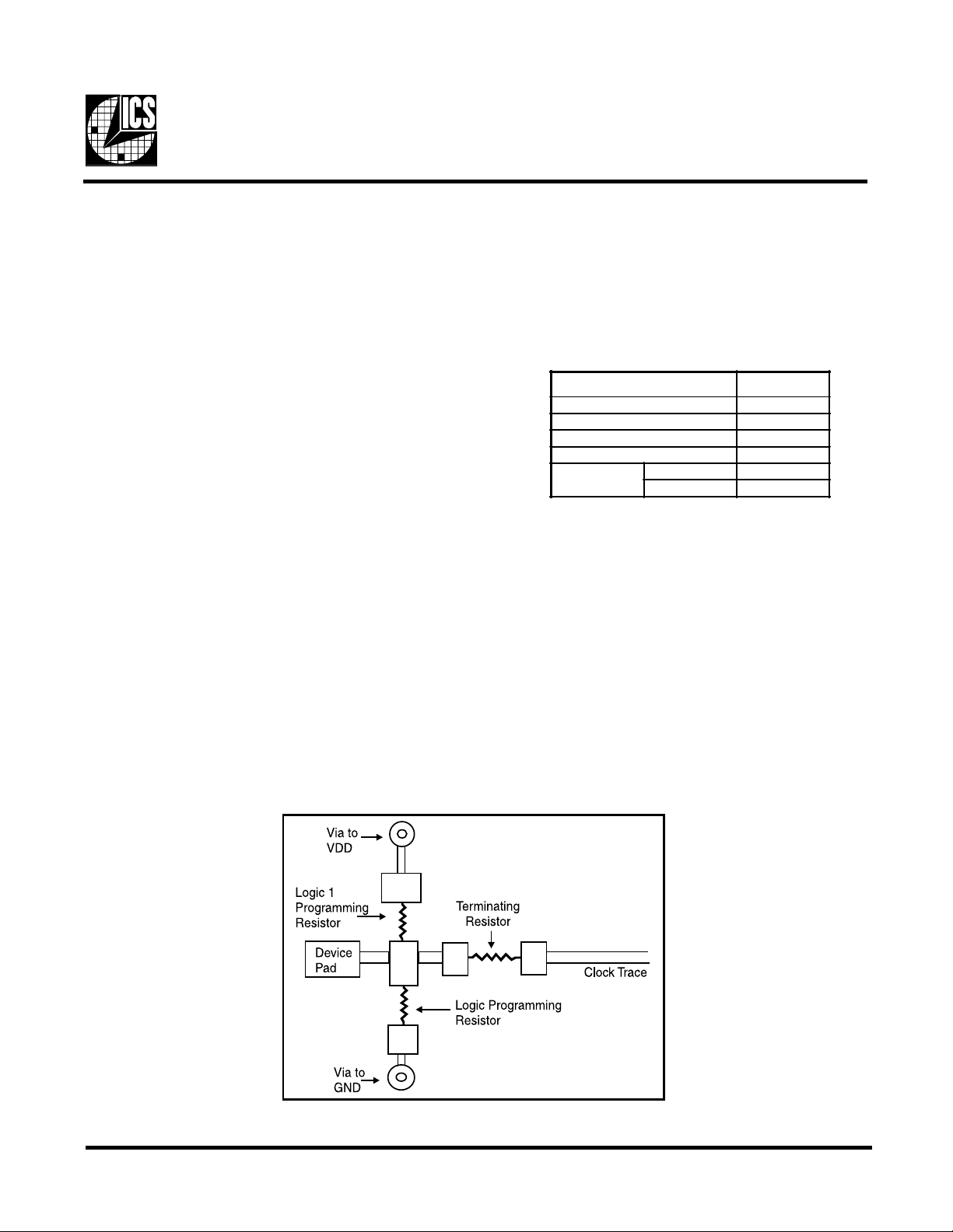
Shared Pin Operation Input/Output Pins
Shared Pin Operation - Input/Output, Pins 5, 28, 12 and
13 on the ICS9169C-231 serve as dual signal functions to
the device. During initial power-up, they act as input pins.
The logic level (voltage) that is present on these pins at
this time is read and stored into a 4-bit internal data latch.
At the end of Power-On reset, (see AC characteristics for
timing values), the device changes the mode of operations
for these pins to an output function. In this mode the pins
produce the specified buffered clocks to external loads.
To program (load) the internal configuration register for
these pins, a resistor is connected to either the VDD (logic
1) power supply or the GND (logic 0) voltage potential. A
10 Kilohm(10K) resistor is used to provide both the solid
CMOS programming voltage needed during the power-up
programming period and to provide an insignificant load
on the output clock during the subsequent operating
period.
Figs. 1 and 2 show the recommended means of
implementing this function. In Fig. 1 either one of the
resistors is loaded onto the board (selective stuffing) to
configure the de vice’s internal logic. Figs. 2a and b provide
a single resistor loading option where either solder spot
tabs or a physical jumper header may be used.
Test Mode Operation
The ICS9169C-231 includes a production test verification
mode of operation. This requires that the FS0 and FS1 pins
be programmed to a logic high and the FS2 pin be
programmed to a logic low(see Shared Pin Operation
section). In this mode the device will output the following
frequencies.
Pin Frequency
REF REF
48MHz REF/2
24MHz REF/4
CPU (1:8) REF2
BUS (1:6)
Note: REF is the frequency of either the crystal connected
between the devices X1and X2 or, in the case of a device
being driven by an external reference clock, the frequency
of the reference (or test) clock on the device’s X1 pin.
BSEL=1 REF/4
BESEL = 0 REF/3
These figures illustrate the optimal PCB physical layout
options. These configuration resistors are of such a large
ohmic value that they do not effect the low impedance
clock signals. The layouts have been optimized to provide
as little impedance transition to the clock signal as possible,
as it passes through the programming resistor pad(s).
Fig. 1
3
Page 4

ICS169C-231
Fig. 2a
Fig. 2b
Fig. 3
4
Page 5

Technical Pin Function Descriptions
ICS169C-231
VDD1
This is the power supply to the internal logic of the device
as well as the following clock output buffers:
A. REF clock output buffers
B. BUS clock output buffers
C. Fixed clock output buffers
This pin may be operated at any voltage between 3.0 and
5.5 volts. Clocks from the listed buffers that it supplies
will have a voltage swing from ground to this level. For the
actual guaranteed high and low voltage levels of these
clocks, please consult the AC parameter table in this data
sheet.
GND
This is the power supply ground return pin for the internal
logic of the device as well as the following clock output
buffers:
A. REF clock output buffers
B. BUS clock output buffers
C. CPU clock output buffers
X1
This pin serves one of two functions. When the device is
used with a crystal, X1 acts as the input pin for the
reference signal that comes from the discrete crystal.
When the device is driven by an external clock signal, X1
is the device’ input pin for that reference clock. This pin
also implements an internal crystal loading capacitor that
is connected to ground. See the data tables for the value of
the capacitor.
X2
This pin is used only when the device uses a Crystal as the
reference frequency source. In this mode of operation, X2
is an output signal that drives (or excites) the discrete
crystal. This pin also implements an internal crystal loading
capacitor that is connected to ground. See the data tables
for the value of the capacitor.
CPU (1:8)
This pin is the clock output that drives processor and other
CPU related circuitry that require clocks which are in tight
skew tolerance with the CPU clock. The voltage swing of
these clocks is controlled by that which is applied to the
VDD pin of the device. See the Functionality table at the
beginning of this data sheet for a list of the specific
frequencies this clock operates at and the selection codes
that are necessary to produce these frequencies.
clocks is controlled by the supply that is applied to the
VDD pin of the device. See the Functionality table at the
beginning of this data sheet for a list of the specific
frequencies that this clock operates at and the selection
codes that are necessary to produce these frequencies.
FS0, FS1, FS2
These pins control the frequency of the clocks at the CPU,
CPUL, BUS, SDRAM, A GP and IOAPIC pins. See the Funtionality table at the beginning of this data sheet for a list
of the specific frequencies that this clock operates at and
the selection codes that are necessary to produce these
frequencies. The device reads these pins at power-up and
stores the programmed selection code in an internal data
latch. (See programming section of this data sheet for
configuration circuitry recommendations.
BSEL
When this pin is a logic 1, it will place the CPU clocks in
the synchronous mode (running at half the frequency of
the Ref). If this pin is a logic 0, it will be in the asynchronous
mode for the CPU clocks and will operate at the
preprogrammed fixed frequency rate. It is a shared pin
and is programed the same way as the Frequency Select
pins.
VDD 2, 3
These are the power supply pins for the CPU clock buffers.
By separating the clock power pins, each group can receive
the appropriate power decoupling and bypassing necessary
to minimize EMI and crosstalk between the individual
signals. VDD2 can be reduced to 2.5V VDD for advanced
processor clocks which will bring CPU (1:6) outputs at 0
to 2.5V output swings.
48 MHz
This is a fixed frequency clock that is typically used to
drive Super I/O peripheral device needs.
24 MHz
This is a fixed frequency clock that is typically used to
drive Keyboard controller clock needs.
VDD4
This power pin supplies the BUS clock buffers.
REF
This is a fixed frequency clock that runs at the same
frequency as the input reference clock (typically 14.31818
MHz) is and typically used to drive Video and ISA BUS
requirements.
BUS (1:6)
This pin is the clock output that is intended to drive the
systems plug-in card bus. The voltage swing of these
VDD5
This power pin supplies the 48/24 MHz clocks.
5
Page 6

ICS169C-231
Absolute Maximum Ratings
Supply Voltage . . . . . . . . . . . . . . . . . . . . . . . . . . 7.0 V
Logic Inputs . . . . . . . . . . . . . . . . . . . . . . . . . . . . GND –0.5 V to VDD +0.5 V
Ambient Operating Temperature . . . . . . . . . . 0°C to +70°C
Storage Temperature. . . . . . . . . . . . . . . . . . . . . –65°C to +150°C
Stresses above those listed under Absolute Maximum Ratings may cause permanent damage to the device. These ratings
are stress specifications only and functional operation of the device at these or any other conditions above those listed
in the operational sections of the specifications is not implied. Exposure to absolute maximum rating conditions for
extended periods may affect product reliability.
Electrical Characteristics at 3.3V
VDD = 3.0 – 3.7 V, TA = 0 – 70°C unless otherwise stated
DC Ch a ract er is tic s
PARAMETER SYMBOL TEST CONDITIONS MIN TYP MAX UNITS
IL
Input Low Voltage
Input High Voltage
Input Low Current
Input High Current
Output Low Current
Output High Current
Output Low Current
Output High Current
Output Low Voltage
Output High Voltage
Output Low Voltage
Output High Voltage
Supply Current
V
IH
V
IL
I
IH
I
1
1
1
1
1
1
1
1
OL
I
OH
I
OL
I
OH
I
OL
V
OH
V
OL
V
OH
V
DD
I
VIN=0V -28.0 -10.5 - µA
DD
VIN=V
OL
V
= 0.8V; for CPU, BUS, Fixed CLKs 16.0 25.0 - mA
OL
V
= 2.0V; for CPU, BUS, Fixed CLKs - -30.0 -14.0 mA
OL
V
= 0.8V; for REF CLK 19.0 30.0 - mA
VOL=2.0V; for REF CLK - -38.0 -16.0 mA
OL
I
= 8mA; for CPU, BUS, Fixed CLKs - 0.3 0.4 V
OH
I
= -8mA; for CPU, BUS, Fixed CLKs 2.4 2.8 - V
OL
I
= 10mA; for REF CLK - 0.3 0.4 V
OH
I
= -15mA; for REF CLK 2.4 2.8 - V
@66.6 MHz; all outputs unloaded - 70 140 mA
- - 0.2V
DD
0.7V
--V
-5.0 - 5.0 µA
DD
V
Note 1: Parameter is guaranteed by design and characterization. Not 100% tested in production.
6
Page 7

ICS169C-231
Electrical Characteristics at 3.3V
VDD = 3.0 – 3.7 V, TA = 0 – 70°C unless otherwise stated
AC Characteristics
PARAMETER SYMBOL TEST CONDITIONS MIN TYP MAX UNITS
Rise Time
Fall Time
Rise Time
Fall Time
Duty Cycle
Jitter, One Sigma
Jitter, Absolute
Jitter, One Sigma
Jitter, Absolute
Input Frequency
Logic Input Capacitance
Crystal Oscillator Capacitance
Power-on Time
Frequency Settling Time
Clock Skew
Clock Skew
Clock Skew
1
1
1
1
1
1
1
1
1
1
1
1
1
1
1
1
1
T
T
T
T
D
T
j1s1
T
jab1
T
j1s2
T
jab2
F
C
C
INX
t
on
t
T
sk1
T
sk2
T
sk3
Note 1: Parameter is guaranteed by design and characterization. Not 100% tested in production.
20pF load, 0.8 to 2.0V
r1
CPU & BUS
20pF load, 2.0 to 0.8V
f1
CPU & BUS
20pF load, 20% to 80%
r2
CPU & BUS
20pF load, 80% to 20%
f2
CPU & BUS
20pF load @ VOUT=1.4V 45 50 60 %
t
CPU & BUS Clocks;
Load=20pF, BSEL=1
CPU & BUS Clocks;
Load=20pF, BSEL=1
- 0.9 1.5 ns
- 0.8 1.4 ns
- 1.5 2.5 ns
- 1.4 2.4 ns
- 50 150 ps
-250 - 250 ps
REF & Fixed CLKs; Load=20pF - 1 3 %
REF & Fixed CLKs; Load=20pF -5 2 5 %
i
Logic input pins - 5 - pF
IN
12.0 14.318 16.0 MHz
X1, X2 pins - 18 - pF
From VDD=1.6V to 1st crossing of
66.6 MHz V
From 1st crossing of acquisition to <
s
1% settling
supply ramp < 40ms
DD
- 2.5 4.5 ms
- 2. 0 4. 0 ms
CPU to CPU; Load=20pF; @1.4V - 150 250 ps
BUS to BUS; Load=20pF; @1.4V - 160 500 ps
CPU to BUS; Load=20pF; @1.4V
(CPU is early)
1 2. 2 4 ns
7
Page 8
ICS169C-231
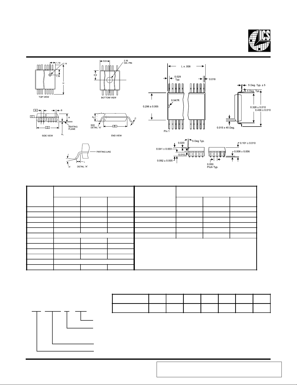
SSOP P ac kage
COMMON
SSOP
SYMBOL
A 0.068 0.073 0.078 14 0.239 0.244 0.249
A1 0.002 0.005 0.008 16 0.239 0.244 0.249
A2 0.066 0.068 0.070 20 0.278 0.284 0.289
B 0.010 0.012 0.015 24 0.318 0.323 0.328
C 0.004 0.006 0.008 28 0.397 0.402 0.407
D See Variations 30 0.397 0.402 0.407
E 0.205 0.209 0.212
e 0.0256 BSC
H 0.301 0.307 0.311
L 0.025 0.030 0.037
N See Variations
∝ 0° 4° 8°
MIN. NOM. MAX. MIN. NOM. MAX.
DIMENSIONS SSOP
VARIATIONS
SOIC P ackage
D
Ordering Information
ICS9169CF-231
ICS9169CM-231
Example:
ICS XXXX F - PPP
Pattern Number (2 or 3 digit number for parts with ROM code patterns)
Packag eType
F=SSOP
M=SOIC
Device Type (consists of 3 or 4 digit numbers)
Prefix
SOIC Pack age (wide bod y)
LEAD COUNT 14L 16L 18L 20L 24L 28L 32L
DIMENSION L 0.354 0.404 0.454 0.504 0.604 0.704 0.804
e = 0.05 BSC
ICS reserves the right to make changes in the device data identified in this publication
without further notice. ICS advises its customers to obtain the latest version of all
8
device data to verify that any information being relied upon by the customer is current
and accurate.
 Loading...