

Page 1
Integrated
Circuit
ICS9159-12
Systems, Inc.
Frequency Generator and Buffers for Mobile Pentium Systems
General Description
The ICS9159-12 generates all clocks required for mobile
microprocessor systems based on Pentium/Mobile Triton
chip sets. Three different reference frequency multiplying
factors are externally selectable with smooth frequency
transitions. These multiplying factors can be customized
for specific plications. A test mode is provided to drive all
clocks directly.
High drive BCLK outputs provide greater than 1V/ns slew
rate into 30pF loads. PCLK outputs provide better than 1V/
ns slew rate into 20pF loads while maintaining ±5% duty
cycle.
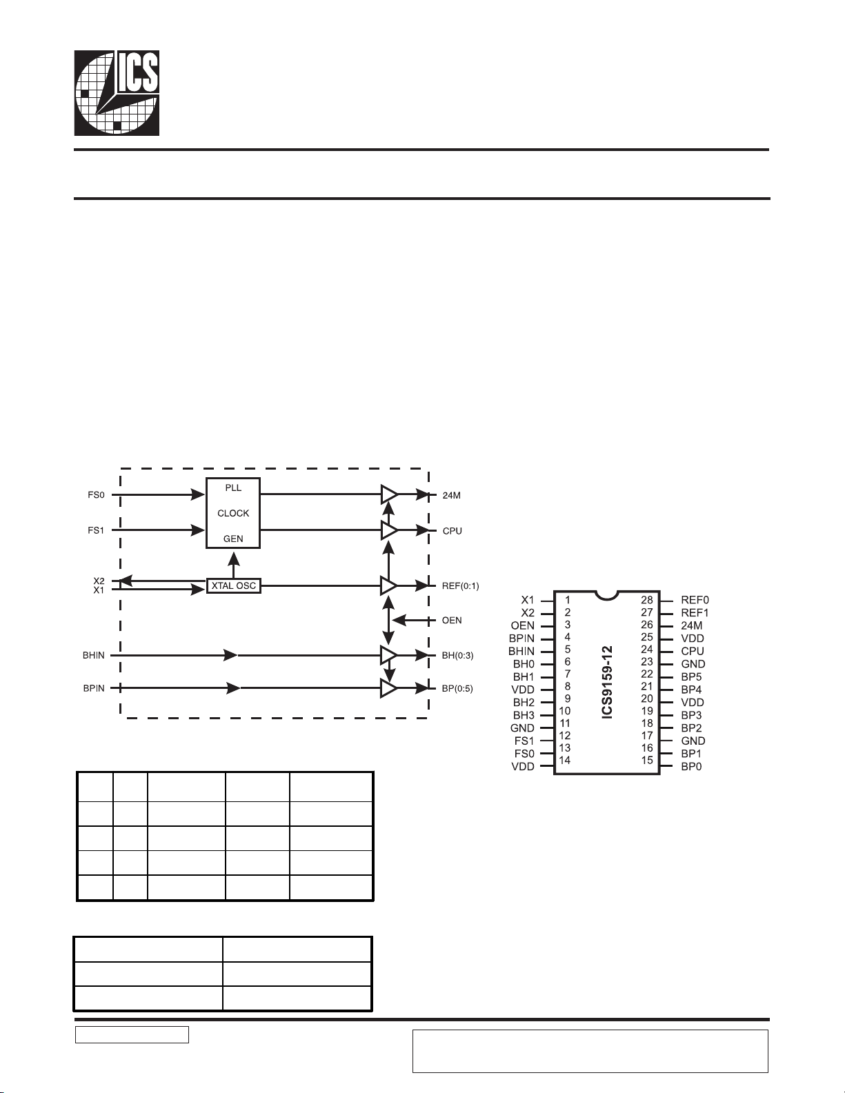
Block Diagram
Features
Generates 14 clocks including processor, disk
and reference
Meets all Pentium/Mobile Triton 82430MX
requirments
Independent buffers provide 4 and 6 clock copies
Buffered clocks skew matched to ±250ps
Buffer inputs are 5V tolerant
Test clock mode eases system design
Selectable multiplying and processor/bus ratios
Custom configurations available
3.0V- 5.5V supply range
28pin, .209" SSOP package
Pin Configuration
Functionality
FS1 FS0 *VCO
0 0 118/17*X1 14.318 50 (49.69)
0 1 65/7*X1 14.318 66. 6 (66.47)
1 0 92/11*X1 14.318 60 (59.87)
1 1 Test mode TCLK TCLK/2
*VCO range is limited form 60 - 200 MHz.
CPU 24M
VCO/2 24 MHz
TCLK/2 TCLK/4
9159-12 Rev B 071797
X1, REF
(MHz)
CPU (MHz)
28-Pin SSOP
Pentium is a trademark of Intel Corporation.
ICS reserves the right to make changes in the device data identified in this publication
without further notice. ICS advises its customers to obtain the latest version of all
device data to verify that any information being relied upon by the customer is current
and accurate.
Page 2
ICS9159-12
Pin Descriptions
PIN NUMBER PIN NAME TYPE DESCRIPTION
8, 25 VDD PWR Power for logic , CPU and fixed frequ ency output buffers.
1X1 IN
2 X2 OUT XTAL output which includes XTAL load capacitance.
3 OEN IN OEN tristates all outputs when low. This input has an internal pull-up device.
4 BPIN IN Input to BPIN(0:5) buffers.
5 BHIN IN Input to BHIN(0:3) buffers.
11, 23 GND PWR Ground for logic, CPU and fixed frequency output buffers.
6, 7, 9, 10 BH(0:3) OUT
13, 12 FS(0:1) IN
14, 20 VDD PWR Power for B CLK output buffers.
15, 16, 18 19,
21, 22
24 CPU OUT
26 24M OUT The 24M clock is fixed at 24 MHz.
28, 27 REF(0:1) OUT
BP(0:5) OUT
XTAL or external reference frequency input. This input includes XTAL load
capacitance and feedback bias for a 10 - 30 MHz XTAL.
Buffered copies of the BHIN input, typically used to drive the PCI device clock
inputs at one half the CPU frequency.
Frequency multiplier select pins. See table below. These inputs have internal pull-up
devices.
Buffered copies of the BPIN input , typically used to drive the host device clock
inputs at the CPU fr equency. 17 VSS PWR Ground f or BCLK output buffers.
The CPU output, which is a multiple of the input reference frequency as shown in
the table above. Duty cy cle is 50/50±5% with a maximum freq uency of 100 MHz.
REF is a buffered copy of the crystal oscillator or reference input clock,
nominally 14.3 1818 MHz.
Note: BCLK buffers cannot be supplied with 5 volts (Pins 14 and 20) if CPU
and fixed frequencies (Pins 1, 8 and 26) are being supplied with 3 volts.
2
Page 3

ICS9159-12
Absolute Maximum Ratings
Supply Voltage .......................................................................................................... 7.0 V
Logic Inputs ....................................................................... GND 0.5 V to VDD +0.5 V
Ambient Operating Temperature ............................................................. 0°C to +70°C
Storage Temperature ........................................................................... 65°C to +150°C
Stresses above those listed under Absolute Maximum Ratings may cause permanent damage to the device. These ratings
are stress specifications only and functional operation of the device at these or any other conditions above those listed
in the operational sections of the specifications is not implied. Exposure to absolute maximum rating conditions for
extended periods may affect product reliability.
Electrical Characteristics at 3.3V
VDD = 3.0 3.7 V
DC Char ac t e r i s t i c s
PARAMETER SYMBOL TEST C ONDI TI ONS MIN TYP MAX UNI T S
Input Low Voltage V
Input High Volt age V
Input Low Current I
Input High Current I
Output Low Current I
Output High Current I
Output Low Current I
Output High Current I
Output Low Voltage V
Outpu t Hi gh Volt a ge V
Output Low Voltage V
Outpu t Hi gh Volt a ge V
Supply Curr ent I
IL --0.2VDD V
IH 0.7VDD --V
IL VIN=0V - 10.5 28.0 µA
IH VIN=VDD -5.0 - 5.0 µA
OL VOL=0.8V; for PCLKS & BCLKS 30.0 47.0 - mA
OH VOL=2.0V; for PCLKS & BCLKS - -66.0 -42.0 mA
OL VOL=0.8V; for fixed CLKs 25.0 38.0 - mA
OH VOL=2.0V; for fixed CLKs - -47.0 -30.0 mA
OL IOL=15mA; for PCLKS & BCLKS - 0.3 0.4 V
OH IOH=-30mA; for PCLKS & BCLKS 2.4 2.8 - V
OL IOL=12.5mA; for fixed CLKs - 0.3 0.4 V
OH IOH=-20mA; for fixed CLKs 2.4 2.8 - V
CC @66.66 MHz; all ou t put s unl oade d - 5 5 110 mA
3
Page 4

ICS9159-12
Electrical Characteristics at 3.3V
VDD = 3.0 3.7 V
PARAMETER SYMBOL TEST CONDITIONS MIN TYP MAX UNITS
Rise Time 0.8 to 2.0V T
Fall Time 2.0 to 0.8V T
Rise Time 20% to 80% T
Fall Time 80% to 20% T
Duty Cycle [CPU] D
Duty Cycle, [REF(0:1)] D
Jitter, One Sigma T
Jitter, Absolute T
Jitter, One Sigma T
Jitter, Absolute T
Input Freque ncy F
Clock Skew Window T
Clock Skew Window T
Clock Skew Window T
r 20pF load - 1.5 3 ns
f 20pF load - 0.9 2 n s
r 20pF l oad - 2 4.5 ns
f 20pF load - 1.8 4 .25 ns
t 20pF load 45 50 55 %
t 20 pF load 40 - 60 %
j1s CPU Clock; Load=20pF, FOUT>25 MHz - 50 150 ps
jab CPU Clock; Load=20pF, FOUT>25 MHz -250 - 250 ps
j1s Fixed CLK; Load=20pF; Comp. to the period - 1 3 %
jab Fixed CLK; Load=20pF; Comp. to the period - 2 5 %
i - 14.318 - M Hz
sk BH to BH; Load=20pF; @1.4V - 50 250 ps
sk BP to BP; Load=20pF; @1.4V - 50 250 ps
sk BH to BP; Load=2 0pF; @1.4V - 100 500 ps
AC Characteristics
4
Page 5

ICS9159-12
COMMON
SYMBOL
MIN. NOM. MAX. MIN. NOM. MAX.
A 0.068 0.073 0.078 14 0.239 0.244 0.249
A1 0.002 0.005 0.008 16 0.239 0.244 0.249
A2 0.066 0.068 0.070 20 0.278 0.284 0.289
B 0.010 0.012 0.015 24 0.318 0.323 0.328
C 0.005 0.006 0.008 28 0.397 0.402 0.407
D See Variations 30 0.397 0.402 0.407
E 0.205 0.209 0.212 34 0.701 0.706 0.711
e 0.0256 BSC 36 0.602 0.607 0.612
H 0.301 0.307 0.311 44 0.701 0.706 0.711
L 0.022 0.030 0.037 48 0.620 0.625 0.630
N See Variations 56 0.720 0.725 0.730
∝
0° 4° 8°
DIMENSIONS
Ordering Information
ICS9159F-12
Example:
ICS XXXX F-PPP
VARIATIONS
D
SSOP Package
Pattern Number(2 or 3 digit number for parts with ROM code patterns)
Package Type
F=SSOP
Device Type (consists of 3 or 4 digit numbers)
Prefix
ICS=Standard Device
ICS reserves the right to make changes in the device data identified in this publication
without further notice. ICS advises its customers to obtain the latest version of all
5
device data to verify that any information being relied upon by the customer is current
and accurate.
 Loading...