

Page 1
Integrated
Circuit
Systems, Inc.
General DescriptionFeatures
ICS9158-07
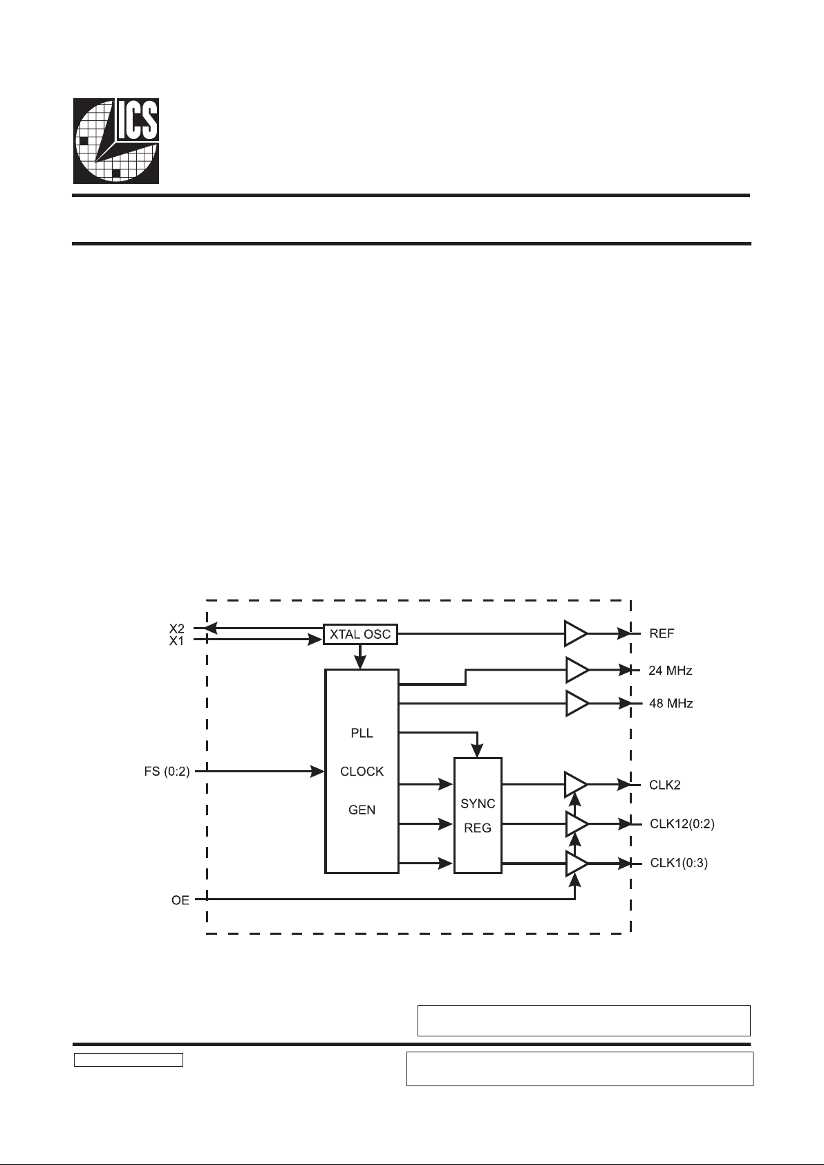
Block Diagram
9158-07 Rev B 053197
Applications
Frequency Generator and Integrated Buffer
The ICS9158-07 is a low-cost frequency generator designed
specifically for desktop and notebook PC applications. Four
copies of the CPU clock are available and four copies of
the BUS clock are available, elimating the need for an
external buffer.
Each high drive (25mA) output is capable of driving a 30pF
load and has a typical duty cycle of 50/50. The clock outputs
are skew-controlled to within ±250ps.
The ICS9158-07 makes a gradual transition between frequencies, so that it meets the Intel cycle-to-cycle timing specification for 486 and Pentium systems.
•8 skew-free, high drive CPU/BUS clocks
•Reference, floppy and keyboard clocks
•±250ps skew between all outputs
•Less than ±250ps absolute jitter
•Outputs can drive up to 30pF load at 1.5V/ns
•50±10% duty cycle
•Compatible with 486 and Pentium CPUs
•On-chip loop filter components
•3.0V - 5.5V supply range
•24-pin SOIC package
Ideal for RISC or CISC systems such as 486, Pentium,™
PowerPC,™ etc., requiring multiple CPU and BUS clocks.
Pentium is a trademark of Intel Corporation.
PowerPC is a trademark of Motorola Corporation.
NOTE: THIS DATA SHEET, ICS9158-07, IS AN ADDENDUM TO THE EXISTING
ICS9158 DATA SHEET. ALL INFORMATION IN THIS DATA SHEET SUPERSEDES
THE DATA FOUND IN THE ORIGINAL ICS9158 DATA SHEET.
ICS reserves the right to make changes in the device data identified in this publication
without further notice. ICS advises its customers to obtain the latest version of all
device data to verify that any
Page 2
2
ICS9158-07
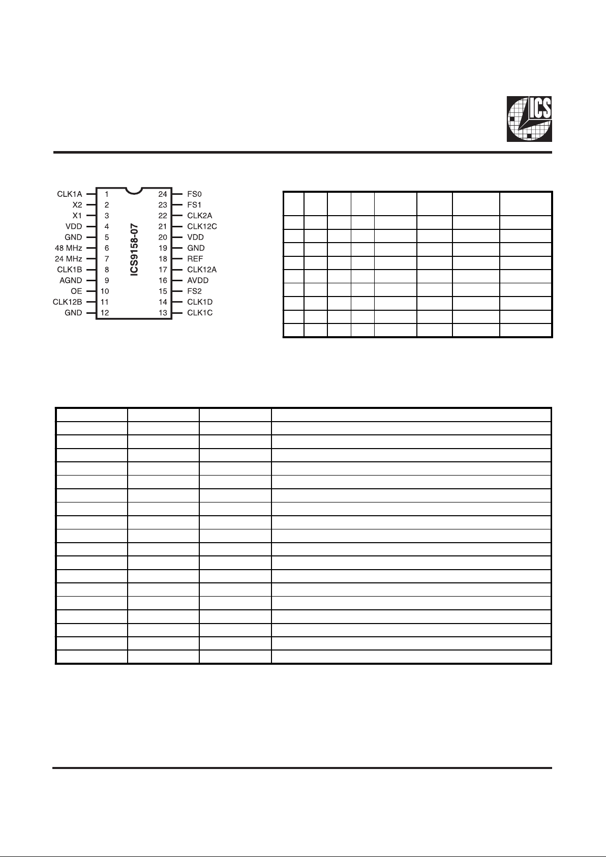
Pin Configuration
Pin Descriptions
24-Pin SOIC
Functionality
VDD=5±10% or 3.3V±10%, TEMP=0-70°C
Note 1: All frequencies in MHz, assuming 14.31818 MHz reference frequency.
Note 2: OE equals Low , tristates CLK2, CLK12(0:2), CLK1(0:3), the REF, 24 MHz
and 48 MHz clocks keep running.
PIN NUMBER PIN NAME TYPE DESCRIPTION
1, 8, 13, 14 CLK1A OUT CPU clock 1 outputs.
2 X2 OUT Crystal connection.
3 X1 IN Crystal connection.
4 VDD PWR Digital POWER SUPPLY (+5V).
5, 12 GND PWR Digital GROUND/
6 48 MHz OUT 48 MHz clock output.
7 24 MHz OUT 24 MHz floppy disk/combination I/O clock output.
9 AGND PWR ANALOG GROUND.
10 OE IN OUTPUT ENABLE. Tristates all cloc k outputs when low.
11, 17, 21, 22 CLK12 OUT CPU clock 12 outputs.
15 FS2 IN CPU clock frequency select 2.
16 AVDD PWR ANALOG power supply (+5V).
18 REF OUT 14.318 MHz reference clock output.
19 GND PWR Digital GROUND.
20 VDD PWR Digital POWER SUPPLY (+5V).
22 CLK2 OUT CPU clock 2 outputs.
23 FS1 IN CPU clock frequency select #1.
24 FS0 IN CPU clock frequency select #0.
OE FS2 FS1 FS0
CLK2
Ratio
CLK2
(Mhz)
CLK1(0:3)
(Mhz)
CLK12(0:2)
(MHz)
1 0 0 0 29/13 X1 31.9 16 31.9
1 0 0 1 29/13 X1 31.9 16 31.9
1 0 1 0 29/13 X1 31.9 16 31.9
1 0 1 1 29/13 X1 31.9 16 31.9
1 1 0 0 14/3 X1 66.8 33.4 66.8
1 1 0 1 7/2 X1 50.1 25 50.1
1 1 1 0 14/3 X1 66.8 33.4 66.8
1 1 1 1 21/5 X1 60.1 30 60.1
0 X X X -- Tristate Tristate Tristate
Page 3

3
ICS9158-07
Electrical Characteristics at 5V
Absolute Maximum Ratings
AVDD, VDD referenced to GND . . . . . . . . . . . . . . . . 7V
Operating temperature under bias. . . . . . . . . . . . . . . . 0°C to +70°C
Storage temperature . . . . . . . . . . . . . . . . . . . . . . . . . . -40°C to +150°C
Voltage on I/O pins referenced to GND. . . . . . . . . . . GND -0.5V to VDD +0.5V
Power dissipation . . . . . . . . . . . . . . . . . . . . . . . . . . . . 0.5 Watts
Stresses above those listed under Absolute Maximum Ratings may cause permanent damage to the device. This is a stress rating
only and functional operation of the device at these or any other conditions above those indicated in the operational sections
of the specifications is not implied. Exposure to absolute maximum rating conditions for extended periods may affect product
reliability.
V
DD
= +5V±10%, TA=0°C to 70°C unless otherwise stated
Note 1: Parameter is guaranteed by design and characterization. Not 100% tested in production.
DC Chara cteristics
PARAMETER SYMBOL TEST CONDITIONS MIN TYP MAX UNITS
Input Low Voltage V
IL
0.8 V
Input High Voltage V
IH
2.0 V
Input Low Current I
IL
VIN=0V -5 5 µA
Input High Current I
IH
VIN=V
DD
-5 5 µ A
Output Low Voltage V
OL
IOL=20.0mA 0.25 0.4 V
Output High Voltage
1
V
OH
IOH=-30mA 2.4 3.5 V
Output Low Current
1
I
OL
VOL=0.8V 45 65 mA
Output High Current
1
I
OH
VOH=2.0V -55 -35 mA
Supply Current I
DD
No load, 80 MH z 43 65 mA
Output Frequenc y Change over
Supply and Temperature
1
F
D
With respect to typical
frequency
0.002 0.01 %
Short circuit current
1
I
SC
Each output clock 25 56 mA
Pull-up resistor value
1
R
PU
Input pin 680 k
Ω
Input Capacitanc e
1
C
i
Except X1, X2 8 pf
Load Capacitanc e
1
C
L
Pins X1, X2 20 pf
Page 4

4
ICS9158-07
Electrical Characteristics
(continued)
V
DD
= +5V±10%, TA=0°C to 70°C unless otherwise stated
Note 1: Parameter is guaranteed by design and characterization. Not 100% tested in production.
AC Charac teristics
PARAMETER SYMBOL TEST CONDITIONS MIN TYP MAX UNITS
Output Rise time, 0.8 to 2.0V
1
t
r
30pf load - 1 2 ns
Rise time, 20% to 80% V
DD
1
t
r
30pf load - 2.5 3 ns
Output Fall time , 2.0 to 0.8V
1
t
f
30pf load - 0.5 1 ns
Fall time, 80% to 20% V
DD
1
t
f
30pf load - 1.5 2 ns
Duty cycle
1
d
t
30pf load 45 50 55 %
Jitter, one sigma
1
t
j1s
As compared with clock
period
-0.52.0%
Jitter, absolute t
jab
-25%
Jitter, absolute t
jab
16-100 MHz cloc ks - 500 ps
Input Frequency f
i
-14.318 MHz
Clock skew between C PU and
2XCPU outputs
T
sk
- 100 250 ps
Frequency Transition time
1
t
ft
From 4 to 50 MH z - 13 20 ms
Page 5

5
ICS9158-07
24-Pin DIP Pac kage
Ordering Information
ICS9158-07N
Example:
ICS XXXX-PPP M
Package Type
N=DIP (Plastic#)
Pattern Number (2 or 3 digit number for parts with ROM code patterns)
Device Type (consists of 3 or 4 digit numbers)
Prefix
ICS, A V=Standard Device
Page 6

6
ICS9158-07
Ordering Information
ICS9158-07M
Example:
ICS XXXX-PPP M
Package Type
M=SOIC
Pattern Number (2 or 3 digit number for parts with ROM code patterns)
Device Type (consists of 3 or 4 digit numbers)
Prefix
ICS, A V=Standard Device
24-Pin SOIC (wide body
LEAD COUNT 24L
DIMENSION L 0.604
ICS reserves the right to make changes in the device data identified in this publication
without further notice. ICS advises its customers to obtain the latest version of all
device data to verify that any
 Loading...