

Page 1
Integrated
Circuit
Systems, Inc.
ICS9147-16
Frequency Generator & Integrated Buffers for PENTIUM
General Description Features
The ICS9147-16 generates all clocks required for high
speed RISC or CISC microprocessor systems such as Intel
PentiumPro. Two different reference frequency multiplying
factors are externally selectable with smooth frequency
transitions. Glitch-free Stop clock control is provided for
CPU and BUS clocks. Complete chip low current mode is
achieved with the Power Down# pin.
High drive BUS outputs typically provide greater than 1 V/
ns slew rate into 30pF loads. CPU outputs typically provide
better than 1V/ns slew rate into 20pF loads while
maintaining
outputs typically provide better than 0.5V/ns slew rates.
Separate buffer supply pins VDDL allow for nominal 3.3V
voltage or reduced voltage swing (from 2.9 to 2.5V) for
CPU (1:4) and IOAPIC outputs.
50±
5% duty cycle. The REF and IOAPIC clock
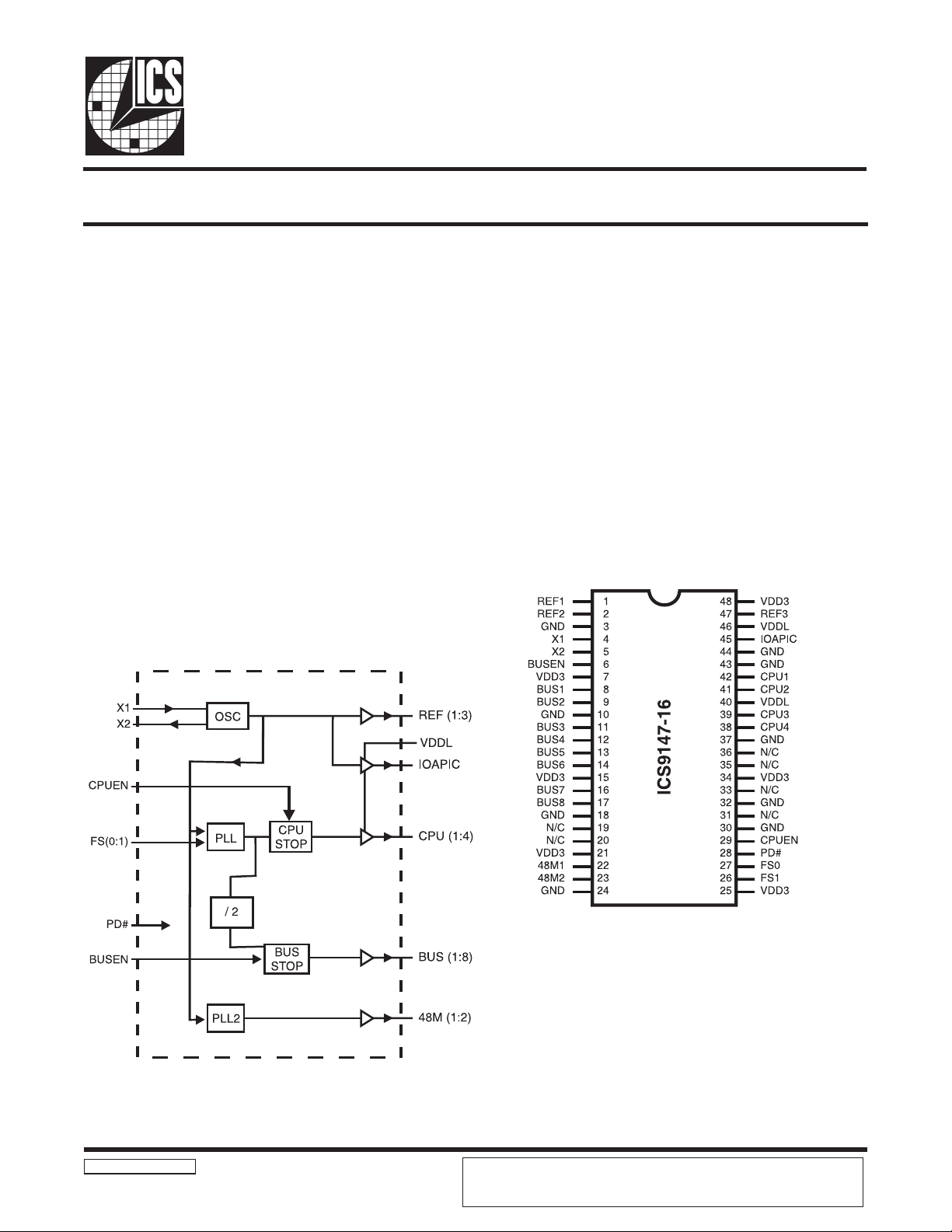
Block Diagram
Generates four processor, eight bus, four 14.31818
MHz, two 48 MHz clocks for USB support.
CPU to BUS clock skew 1 to 4ns (CPU early)
Synchronous clocks skew matched to 250ps window on
CPU and 500ps window on BUS.
Selectable multiplying ratios
Glitch free stop clock controls CPUEN and BUSEN
3.0V 3.7V supply range, 2.5V to VDD supply range for
CPU (1:4) clocks and IOAPIC clock.
48-pin SSOP package
Pin Configuration
TM
9147-16 Rev A 072897P
48-Pin SSOP
Pentium is a trademark of Intel Corporation
ICS reserves the right to make changes in the device data identified in this
publication without further notice. ICS advises its customers to obtain the latest
version of all device data to verify that any information being relied upon by the
customer is current and accurate.
Page 2
ICS9147-16
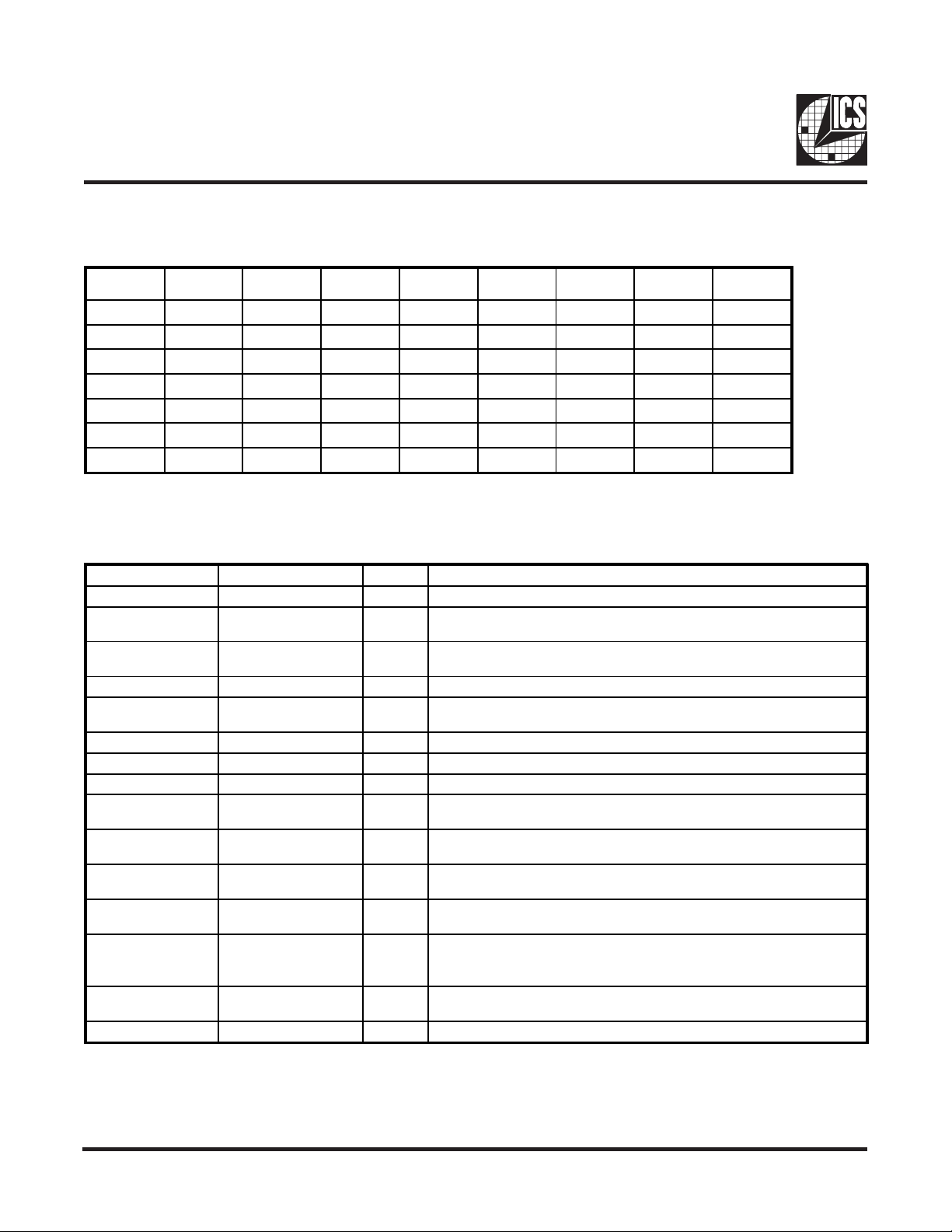
Functionality
PD# BUSEN CPUEN FS1 FS0 CPU (1:4) BUS
11100TristateTristateTristateTristate
11101603014.3181848
1111066.633.314.3181848
11111REF/2REF/4REFREF/2
1 1 0 X X LOW Running 14.31818 48
1 0 1 X X Running LOW 14.31818 48
0XXXXLOWLOWLOWLOW
REF
IOAPIC
Pin Descriptions
PIN NUMBER PIN NAME TYPE DESCRIPTI ON
1, 2, 47 REF1, REF2, REF3 OUT 14.318 MHz reference clock outputs.
3, 10, 18, 24, 30, 32,
37, 43, 44
4X1 IN
5 X2 OUT Crystal output, has internal crystal load capacitor
8, 9, 11, 12, 13, 14,
16, 17
26, 27 FS (0:1) IN Select pin for enabling CPU and BUS clock frequencies.*
7, 15, 21, 25, 34, 48 VDD3 PWR Core and Buffer output clock power supply.
22, 23 48M (1:2) O UT 48 MHz clock output
28 PD# I N
29 CPUE N IN
38, 39, 41, 42 CPU (1:4) OU T
6BUSEN IN
45 IOAPIC OUT
40, 46 VDDL P WR
19, 20, 31, 33, 36 N/C - No connection internally to these pi ns.
GND PWR Ground.
Crystal input, has internal crystal load capacitor, and feedback resistor
from X2. Nominally 14.31818MHz.
BUS (1:8) OUT BUS clock outputs, operates synchronously at CPU/2.
Device power down input, stops outputs low and shuts off crystal
oscillator and PLLs when low.*
Output enable for all CPU clocks, a logic low will Stop low all CPU
clocks.*
CPU clock output clocks, operates at VDDL supply voltage (with
IOAPIC), either nominal 3.3V VDD or reduced voltage 2.9 to 2.5V.
Output enable for all BUS clock, a logic low will stop Low all Bus
clocks.*
IOAPIC clock output. (14.318 MHz), operates at VDDL supply voltage
with CPU (1:4) , either nomi nal 3.3V VDD or red uced voltage
2.9 to 2.5V.
Power supply for CPU and IOAPIC block buffers, operates at nominal
3.3V VDD or reduced voltage 2.9 to 2.5V.
48
(MHz)
* Has internal pull-up to V
DD3
.
2
Page 3

ICS9147-16
Absolute Maximum Ratings
Supply Voltage . . . . . . . . . . . . . . . . . . . . . . . . . . 7.0 V
Logic Inputs . . . . . . . . . . . . . . . . . . . . . . . . . . . . GND 0.5 V to VDD +0.5 V
Ambient Operating Temperature . . . . . . . . . . 0°C to +70°C
Storage Temperature . . . . . . . . . . . . . . . . . . . . . 65°C to +150°C
Stresses above those listed under Absolute Maximum Ratings may cause permanent damage to the device. These ratings
are stress specifications only and functional operation of the device at these or any other conditions above those listed
in the operational sections of the specifications is not implied. Exposure to absolute maximum rating conditions for
extended periods may affect product reliability.
Electrical Characteristics at 3.3V
V
DDL=VDD3
Input Low Voltage V
Input High Voltage V
Input Low Current I
Input High Current I
Output Low Current I
Output High Current
Output Low Current I
Output High Current I
Output Low Current I
Output High Current
Output Low Voltage
Output High Voltage
Output Low Voltage V
Output High Voltage V
Output Low Voltage V
Output High Voltage V
Supply Current I
Supply Current I
Note 1: Parameter is guaranteed by design and characterization. Not 100% tested in production.
=3.0 3.7 V, TA = 0 70° C unless otherwise stated
DC Characteristics
PARAMETER SYMBOL TEST CONDITIONS MIN TYP MAX UNITS
IL - - 0.2VDD V
IH 0.7VDD --V
IL VIN = 0V -28.0 -10.5 - µA
IH V IN = VDD -5.0 - 5.0 µ A
VOL = 0.8V;
OL1
for BUS & REF1
(and CPU & IOAPIC at VDDL= 3.0
to 3.7V)
VOH = 2.0V;
I
OH1a
I
OH1b
OL2 VOL = 0.8V; REF (2:3), 48 CL Ks 8.0 13.0 - mA
OH2 VOH = 2.0V; REF (2:3), 48 CLKs - -11.0 -7.0 mA
OL3
OH3a
I
I
OH3b
for BUS & REF1
(and IOAPIC at V
DDL = 3.0 to 3.7 V)
VOH = 2.0V; for CPU @
VDDL = 3.0 to 3.7V
VOL=0.8V; for CPU at
V
DDL = 2.5V
VOH = 2.0V; for CPU at
V
DDL = 2.5V
VOH = 2.0V; for IOAPIC @
VDDL = 2.5V
IOL = 10mA;
V
OL1
for BUS & REF1
(and CPU at V
DDL = 3.0 to 3.7V)
IOH = -10mA;
OH1
V
OL2 IOL = 4mA; REF (2:3), 48 CLKs - 0.25 0.4 V
OH2 IOH = -4mA; REF (2:3), 48 CLKs 2.4 2.6 - V
OL3
OH3
DD @66.6 MHz; all outputs unloaded - 70 140 mA
DDPD PD# = Low 230 500 µ A
for BUS & REF1
(and CPU at V
DDL = 3.0 to 3.7V)
IOL = 8mA; for CPU at
V
DDL = 2.5V
IOH = -8mA; for CPU at
VDDL = 2.5V
19.0 30.0 - mA
- -28.0 -16.0 mA
-45.0 -27.0 mA
19.0 30.0 - mA
- -12.5 -9.5 mA
-13.0 -10.0 mA
- 0.22 0.4 V
2.4 2.8 - V
- 0.25 0.4 V
2.1 2.25 - V
3
Page 4

ICS9147-16
Electrical Characteristics at 3.3V
V
DDL=VDD3
=3.0 3.7 V, TA = 0 70° C unless otherwise stated
AC Characteristics
PARAMETER SYMBOL TEST CONDITIONS MIN TYP MAX UNITS
Rise Time
Fall Time
Rise Time
Fall Time
Rise Time
Fall Time
Rise Time
Fall Time
Rise Time
Fall Time
Duty Cycle
Duty Cycle
Jitter, One Sigma
Jitter, Absolute
Jitter, One Sigma
Jitter, Absolute
Input Frequency
Logic Input Capacitance
Oscillator Input Capacitance
Power-on Time
Clock Skew
Clock Skew
Clock Skew
Clock Skew
1
1
1
1
1
1
1
1
1
1
1
1
1
1
1
1
1
1
1
1
1
1
1
1
Note 1: Parameter is guaranteed by design and characterization. Not 100% tested in production.
Tr1a 20pF load, 0.8 to 2.0V CPU - 0.9 1.2 ns
Tf1a 20pF load, 2.0 to 0.8V CPU - 0.8 1.2 ns
Tr1b
Tf1b
Tr2
Tf2
Tr3
Tf3
Tr4
Tf4
CL=20pF, VDD=2.5V
0.8 to 2.0V CPU
CL=20pF, VDD=2.5V
2.0 to 0.8V CPU
30pF load, 0. 8 to 2.0V
BUS & REF1
30pF load, 2. 0 to 0.8V
BUS & REF1
20pF load, 0. 8 to 2.0V
48 clock & REF (2 :3)
20pF load, 2. 0 to 0.8V
48 clock & REF (2 :3)
20pF load, 0. 8 to 2.0V , IOAPI C with
VDDL = 2.5V
20pF load, 2.0 to 0.8V, IOAPIC with
VDDL = 2.5V
-1.01.2ns
-1.01.2 ns
-0.91.6ns
-0.81.5 ns
-1.42.4 ns
-1.82.4 ns
--1.6 ns
--1.6 ns
Dt1 20pF load @ VOUT=1 .4V 45 50 55 %
Dt2
Tjis1
Tjab1
REF (1:3) Load = 20pF REF 2, 3
Load = 47pF REF1
CPU & Fixed BUS Load=20pF,
BUS; Load = 30pF
CPU & Fixed BUS Load=20pF,
BUS; Load = 30pF
40 45 50 %
- 50 150 ps
-250 - 250 ps
Tjis2 REF1; Load = 47pF - 55 250 ps
Tjab2 REF1; Load = 47pF -500 200 500 ps
Fi 12.0 14.318 16.0 MHz
CIN Logic input pins - 5 - pF
CINX X1, X2 pins - 18 - pF
ton
Tsk1
From VDD=3.0V to 1st crossing of
66.6 MHz VDD supply ramp < 1 ms
CPU to CPU; Load=20pF; @1.4V
(Same VDD)
-1.53.0 ms
- 1 50 250 ps
Tsk2 BUS to BUS; Load=20pF; @1.4V - 300 500 ps
Tsk3
CPU to BUS; Load=20pF; @1.4V
(CPU is early) (All at 3.3V)
13.3 4 ns
Tsk4 CPU @ 2.5V to B US @ 3.3V 1 4 ns
T
sk5 REF @ 3. 3V to IOAPIC @ 2.5V 1.5 ns
4
Page 5

Recommended PCB Layout for ICS9147-16
ICS9147-16
NOTE:
This PCB Layout is based on a 4 layer board with an internal Ground (common) and Vcc plane. Placement of
components will depend on routing of signal trace. The 0.1uf Capacitors should be placed as close as possible
to the Power pins. Placement on the backside of the board is also possible. The Ferrite Beads can be replaced
with 10-15ohm Resistors. For best results, use a Fixed Voltage Regulator between the main (board) Vcc and the
different Vdd planes.
5
Page 6

ICS9147-16
SSOP Package
SYMBOL COMMON DIMENSIONS VARIATIONS D N
MIN. NOM. MAX. MIN. NOM. MAX.
A .095 .101 .110 AC .620 .625 .630 48
A1 .008 .012 .016
A2 .088 .090 .092
B .008 .010 .0135
C.005- .010
D See Variations
E .292 .296 .299
e0.025 BSC
H .400 .406 .410
h .010 .013 .016
L .024 .032 .040
N See Variations
∝
X .085 .093 .100
0° 5° 8°
Ordering Information
ICS9147F-16
Example:
ICS XXXX F - PPP
Pattern Number (2 or 3 digit number for parts with ROM code patterns)
Package Type
F=SSOP
Device Type (consists of 3 or 4 digit numbers)
Prefix
ICS = Standard Device
ICS reserves the right to make changes in the device data identified in this
publication without further notice. ICS advises its customers to obtain the latest
6
version of all device data to verify that any information being relied upon by the
customer is current and accurate.
 Loading...