

Page 1
Integrated
Circuit
Systems, Inc.
ICS9147-14
Frequency Generator & Integrated Buffers for PENTIUM/Pro
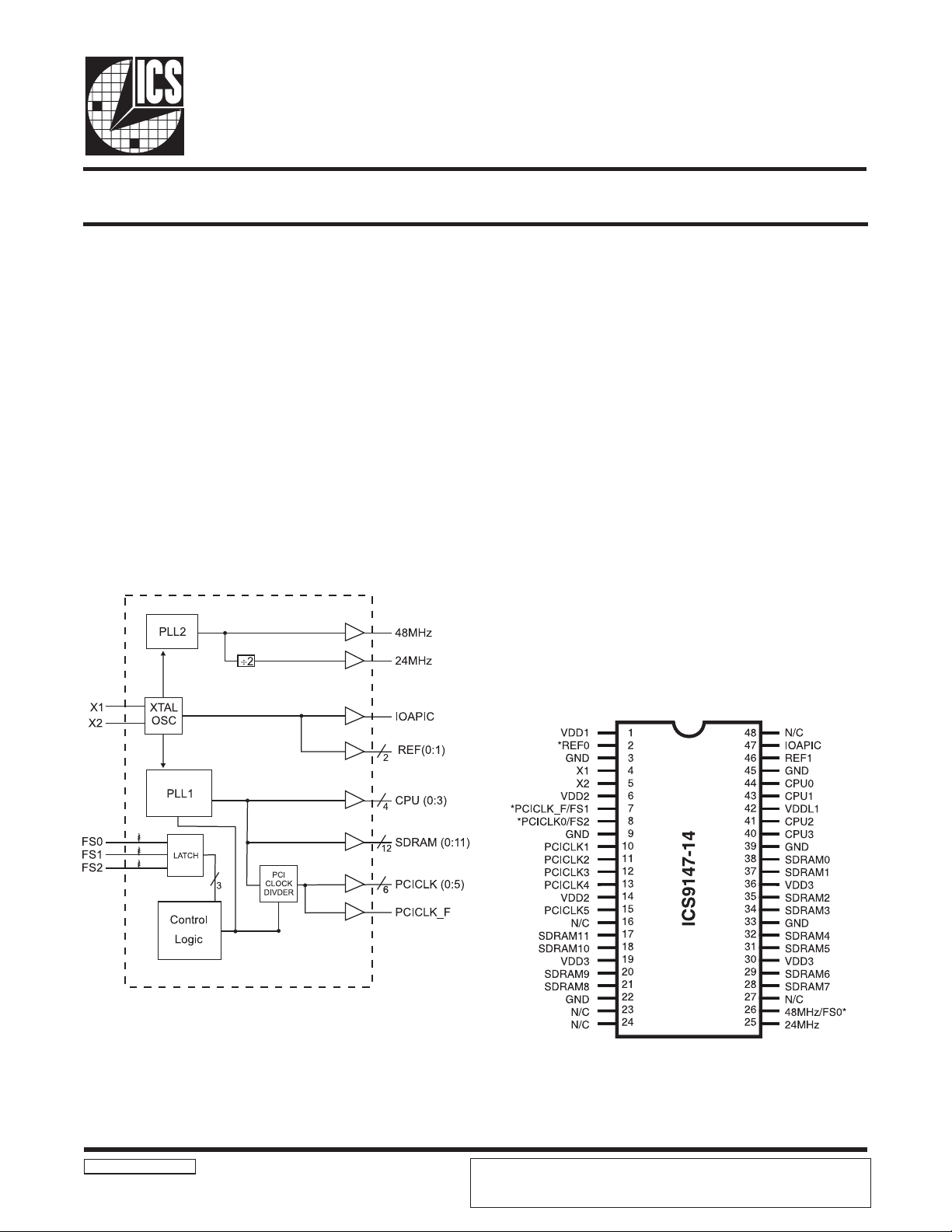
General Description Features
The ICS9147-14 generates all clocks required for high speed
RISC or CISC microprocessor systems such as Intel
PentiumPro. Two bidirectional I/O pins (FS1,FS2) are latched
at power-on to the functionality table, with FS0 selectable in
real-time to toggle between conditions.
High drive PCICLK and SDRAM outputs typically provide
greater than 1 V/ns slew rate into 30 pF loads. CPU outputs
typically provide better than 1V/ns slew rate into 20pF loads
while maintaining
typically provide better than 0.5V/ns slew rates. Seperate
buffers supply pins VDDL1 allow for 3.3V or reduced voltage
swing (from 2.9 to 2.5V) for CPU (0:3) and IOAPIC outputs.
50 ±
5% duty cycle. The REF clock outputs
Block Diagram
Four copies of CPU clock
Twelve SDRAM (3.3 V TTL), usable as AGP clocks
Seven copies of PCICLK clock (synchronous with CPU
clock/2 or CPU/2.5 for 75 and 83.3 MHz CPU)
CPU clocks to PCICLK clocks skew 1-4ns, center 2.6ns.
One IOAPIC clock @14.31818 MHz
Two copies of Ref. clock @14.31818 MHz
Ref. 14.31818 MHz Xtal oscillator input
Separate V
buffers to allow 2.5V output (or Std. Vdd)
One each 48/ 24 M Hz (3.3 V TT L)
3.3V outputs: SDRAM, PCI, REF, 48/24MHz.
2.5V or 3.3V outputs: CPU, IOAPIC.
20 ohm CPU clock output impedance
20 ohm PCI clock output impedance
1.5ns rise time (30 pF loading)
±250 ps CPU, PCI clock skew
350ps (cycle by cycle) CPU jitter
2ms Power up clock stable time
45-55% Clock duty cycle
48 pin 300 mil SSOP package
3.0V 3.7V supply range w/2.5V compatible outputs
for four CPU and single IOAPIC output
DDL1
TM
Power Groups
VDD1 = REF (0:1), X1, X2, 24MHz, 48MHz
VDD2 = PCICLKF, PCICLK(0:5)
VDD3 = SDRAM (0;11)
VDDL1 = CPUCLK (0:3)
Pin Configuration
48-Pin SSOP
* Internal Pull-up Resistor of
300K to 3.3V on indicated inputs
Pentium is a trademark of Intel Corporation
9147-14 Rev B 071897P
ICS reserves the right to make changes in the device data identified in this
publication without further notice. ICS advises its customers to obtain the latest
version of all device data to verify that any information being relied upon by the
customer is current and accurate.
Page 2
ICS9147-14
Pin Descriptions
PIN NUMBER PIN NAME TYPE DESCRIPTION
1 VDD1 P WR Ref (0:2), XTAL, 24MHz, 48MHz power supply
2 REF0 OU T 14.318 Mhz refere nce clock.
3,9,22, 33,39,45 GND PW R Gr oun d
4X1 IN
5 X2 OUT Crystal output nominally 14.318MHz. Has internal load cap
16,23,24,
27,48
N/C - Pins are not internally connected
6,14 VDD2 P WR Supply for PCICLK_F and PCIC LK (0:5)
7
8
10, 11, 12, 13
15
PCICLK_F
FS1*
PCICLK0
FS2*
PCICLK(1:4)
PCICLK5
OUT
IN
OUT
IN
OUT
OUT
17, 18, 20, 21,
28, 29, 31, 32,
SDRAM (0:11)
OUT
34, 35,37,38
19,30,36
25
26
40, 41, 43, 44
42
46 REF1 OUT 14.318 Mhz reference clock.
VDD3
24MHz
48MHz
FS0*
CPUCLK(0:3 )
VDDL1
PWR
OUT
OUT
IN
OUT
PWR
47 IOAPIC OUT IOAPIC clock output . Powered by VDDL1.
Crystal input has internal load cap and feedback
resistor from X2
Free running PCI clock
Frequency select pin. *
PCI clock output.
Frequency select pin. *
PCI clock outputs
PCI clock output.
SDRAM clock outputs.
Supply for SDRAM (0:11)
24MHz output clock
48MHz output clock
Frequency select pin
CPU clock outputs, powered by VDD1
Supply for CPU (0:3) and IOAPIC clock, can be 2.5 or 3.3V
* Internal Pull-up Resistor of 120K to 3.3V on indicated inputs
Functionality
3.3v±10% 0-70°c
Crystal (X1, X2 = 14.3181MHz
FS2 FS1 FS0 CPU, SDRAM(MHz) PCICLK (MHz)
0 0 0 50.0 25.0 14.318
0 0 1 75.0 32.0 14.318
0 1 0 33.3 16.65 14.318
0 1 1 68.5 34.25 14.318
1 0 0 55.0 27.5 14.318
1 0 1 75.0 37.5 14.318
1 1 0 60.0 30.0 14.318
1 1 1 66.8 33.4 14.318
2
REF, IOAPIC
(MHz)
Page 3
ICS9147-14
Absolute Maximum Ratings
Supply Voltage . . . . . . . . . . . . . . . . . . . . . . . . . . 7.0 V
Logic Inputs . . . . . . . . . . . . . . . . . . . . . . . . . . . . GND 0.5 V to VDD +0.5 V
Ambient Operating Temperature . . . . . . . . . . . . 0°C to +70°C
Storage Temperature . . . . . . . . . . . . . . . . . . . . . 65°C to +150°C
Stresses above those listed under Absolute Maximum Ratings may cause permanent damage to the device. These ratings are
stress specifications only and functional operation of the device at these or any other conditions above those listed in the
operational sections of the specifications is not implied. Exposure to absolute maximum rating conditions for extended
periods may affect product reliability.
Electrical Characteristics at 3.3V
VDD = 3.0 3.7 V, TA = 0 70° C unless otherwise stated
DC Characteri stics
PARAMETER SYMBOL TEST CONDITIONS MIN TYP MAX UNITS
Input Low Voltage V
Input Hi gh Voltage V
Output Lo w Current
Output Hi gh Current
Output Lo w Current
Output Hi gh Current
Output Lo w Current
Output Hi gh Current
Output Low Voltage
Output Hi gh Voltage
Output Low Voltage
Output Hi gh Voltage
Output Low Voltage
Output Hi gh Voltage
1
1
1
1
1
1
1
1
1
1
1
1
Supply Current I
Pullup Resistor
1
IL Latched in puts - - 0 .8 V
IH Latched inputs 2.0 - - V
IOL1
IOH1
IOL2
IOH2
IOL3
IOH3
VOL=0.8V;
for SDRAM, PCICLK
VOH=2.0V;
for SDRAM PCICLK
VOL=0.8V; 24, 48 CLKs, CPU, REF
& IOAPIC
VOH=2.0V; 24, 48 CLKs, CPU,
REF & IOAPIC
VOL=0.8V; for CPU at
VDDL = 2.5V
VOH = 1.7V; for CPU at
VDDL = 2.5V
IOL = 10mA;
VOL1
for PCICLK, SDRAM
IOH = -10mA;
VOH1
VOL2
VOH2
VOL3
VOH3
DD @66.6 MHz; all outputs unloaded - 70 120 mA
RPU1
for SDRAM, PCICLK
IOL = 8mA; for fixed CLKs, CPU,
REF & IOAPIC
IOH = -8mA; for fixed CLKs, CPU,
REF & IOAPIC
IOL = 5mA; for CPU at
VDDL = 2.5V
IOH = -5mA; for CPU at
VDDL = 2.5V
FS0, FS1 FS2 inputs 150 300 450 K ohm
19.0 30.0 - mA
- -26.0 -16.0 mA
16.0 25.0 - mA
- -22.0 -14.0 mA
10.0 18.0 - mA
- -14.0 -8.0 mA
-0.30.4V
2.4 2.8 - V
-0.30.4V
2.4 2.8 - V
- 0.25 0 .4 mA
2.1 2.25 - mA
Note 1: Parameter is guaranteed by design and characterization. Not 100% tested in production.
3
Page 4

ICS9147-14
Electrical Characteristics at 3.3V
VDD = 3.0 3.7 V, TA = 0 70° C unless otherwise stated
AC Characteristics
PARAMETER SYMBOL TEST CONDITIONS MIN TYP MAX UNITS
Rise Time
Fall Time
Rise Time
Fall Time
Rise Time
Fall Time
Rise Time
Fall Time
Duty Cycle
Duty Cycle
Jitter, One Sigma
Jitter, Absolute
Jitter, Cycle to Cycle T
Jitter, One Sigma
Jitter, Absolute
Input Frequency
Logic Input Capacitance
Crystal Oscillator Capacitance
Power-on Time
Clock Skew
Clock Skew
Clock Skew
1
1
1
1
1
1
1
1
1
1
1
1
1
1
1
1
1
1
1
1
1
Tr1
Tf1
Tr2
Tf2
Tr3 20pF load, 0. 8 to 2.0V PCI, S DRAM - 0.9 1.5 ns
Tf3 20pF load, 2. 0 to 0.8V PCI, S DRAM - 0.8 1.4 ns
Tr4
Tf4
Dt
DT2
Tjis1
Tjab1
jc-c CPU - 200 350 ps
Tjis2 Fixed CLK; Load=20pF - 1 3 %
Tjab2 Fixed CLK; Load=20pF -5 2 5 %
Fi 12.0 14.318 16.0 MHz
CIN Logic input pins - 5 - pF
CINX X1, X2 pins - 18 - pF
ton
Tsk1
Tsk2
Tsk3
Note 1: Parameter is guaranteed by design and characterization. Not 100% tested in production.
20pF load, 0. 8 to 2.0V
CPU, IOAPIC, Fixed & REF
20pF load, 2. 0 to 0.8V
CPU, IOAPIC, Fixed & REF
20pF load, 20% t o 80%
CPU, IOAPIC, Fixed & REF
20pF load, 80% t o 20%
CPU, IOAPIC, Fixed& REF
20pF load, 0.4 to 2.0V , CPU and
IOAPIC with VDDL = 2.5V
20pF load, 2.0 to 0.4V, CPU and
IOAPIC with VDDL = 2.5V
20pF load @ VOUT=1.4 V
All clocks except RE F
20pF load @ VOUT=1.4 V
REF outputs
CPU & PCICLK Clocks; Load=20pF,
SDRAM; Load = 30pF
CPU & PCICLK Clocks; Load=20pF,
SDRAM; Load = 30pF
From VDD=1.6V to 1st crossing of
66.6 MHz VDD supply ramp < 40ms
CPU to CPU or PCI to PCI;
Load=20pF; @1.4V (Same VDD)
SDRAM to SDRAM;
Load=20pF; @1.4V
CPU to PCI CLK; Load =20pF; @1.4 V
(CPU is early)
-0.91.5ns
-0.81.4 ns
-1.52.5ns
-1.42.4 ns
--3.0 ns
--2.0 ns
45 50 55 %
40 50 60 %
- 50 150 ps
-250 - 250 ps
-2.54.5 ms
- 150 250 ps
- 300 500 ps
1 2.1 4 ns
4
Page 5

Shared Pin Operation Input/Output Pins
ICS9147-14
Pins 7, 8 and 26 on the ICS9147-14 serve as dual signal
functions to the device. During initial power-up, they act
as input pins. The logic level (voltage) that is present on
these pins at this time is read and stored into a 4-bit
internal data latch. At the end of Power-On reset, (see AC
characteristics for timing values), the device changes the
mode of operations for these pins to an output function.
In this mode the pins produce the specified buffered
clocks to external loads.
To program (load) the internal configuration register for
these pins, a resistor is connected to either the VDD
(logic 1) power supply or the GND (logic 0) voltage
potential. A 10 Kilohm(10K) resistor is used to provide
both the solid CMOS programming voltage needed during
the power-up programming period and to provide an
insignificant load on the output clock during the subsequent
operating period.
Figs. 1 and 2 show the recommended means of
implementing this function. In Fig. 1 either one of the
resistors is loaded onto the board (selective stuffing) to
configure the devices internal logic. Figs. 2a and b provide
a single resistor loading option where either solder spot
tabs or a physical jumper header may be used.
These figures illustrate the optimal PCB physical layout
options. These configuration resistors are of such a large
ohmic value that they do not effect the low impedance
clock signals. The layouts have been optimized to provide
as little impedance transition to the clock signal as possible,
as it passes through the programming resistor pad(s).
Fig. 1
5
Page 6

ICS9147-14
Fig. 2a
Fig. 2b
6
Page 7

ICS9147-14
SYMBOL COMMON DIMENSIONS VARIATIONS D N
MIN. NOM. MAX. MIN. NOM. MAX.
A .095 .101 .110 AC .620 .625 .630 48
A1 .008 .012 .016
A2 .088 .090 .092
B .008 .010 .0135
C.005- .010
D See Variations
E .292 .296 .299
e0.025 BSC
H .400 .406 .410
h .010 .013 .016
L .024 .032 .040
N See Variations
∝
X .085 .093 .100
0° 5° 8 °
Ordering Information
ICS9147F-14
Example:
ICS XXXX F - PPP
SSOP Package
Pattern Number (2 or 3 digit number for parts with ROM code patterns)
Package Type
F=SSOP
Device Type (consists of 3 or 4 digit numbers)
Prefix
ICS, AV = Standard Device
ICS reserves the right to make changes in the device data identified in this
publication without further notice. ICS advises its customers to obtain the latest
7
version of all device data to verify that any information being relied upon by the
customer is current and accurate.
 Loading...