

Page 1
Integrated
Circuit
ICS9147-03
Systems, Inc.
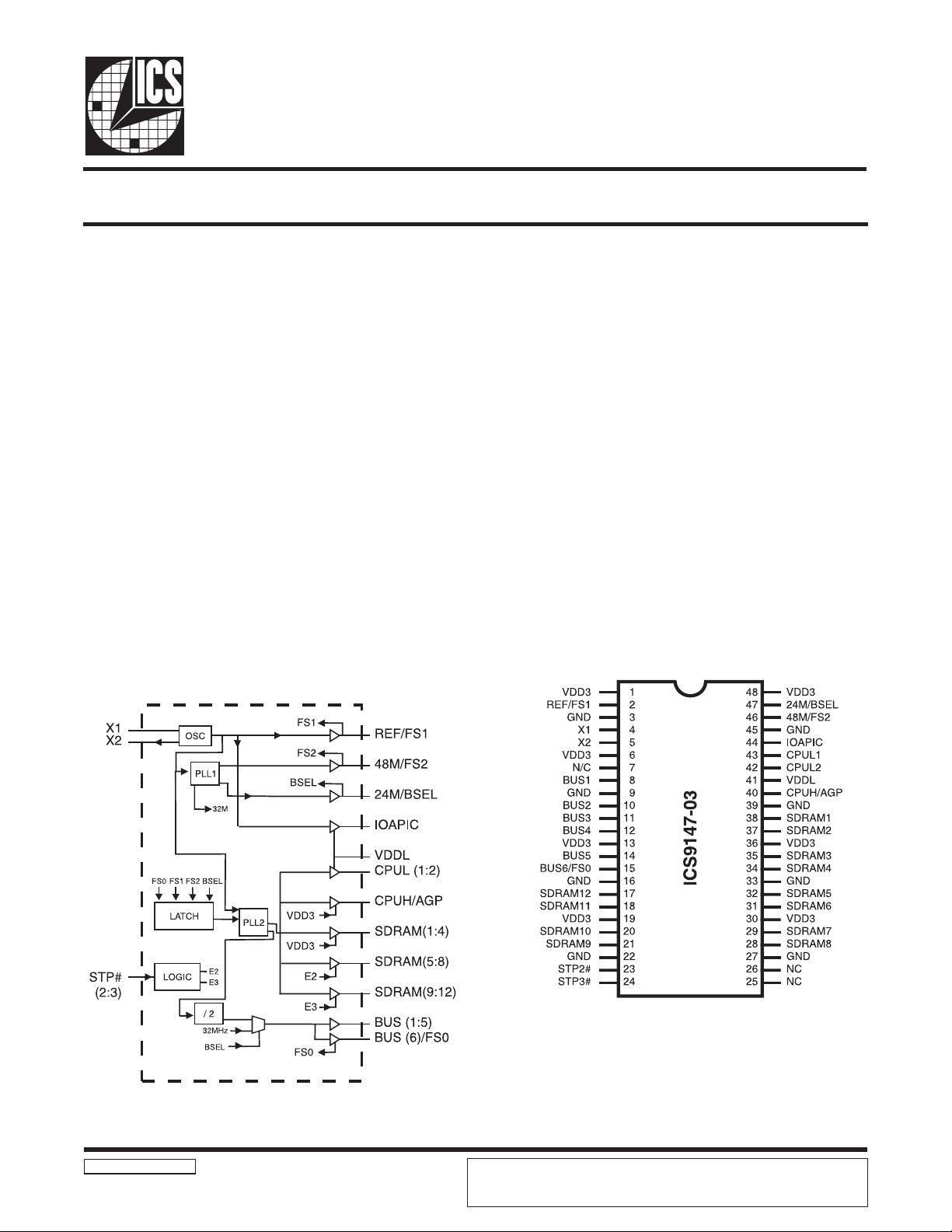
Frequency Generator & Integrated Buffers for 686 Series CPUs
General Description Features
The ICS9147-03 generates all clocks required for high
speed RISC or CISC microprocessor systems such as Intel
PentiumPro, AMD or Cyrix processors. Four bidirectional I/O
pins (FS0, FS1, FS2, BSEL) are latched at power-on to the
functionality table. The Six BUS clocks can be selected as
either synchronous at 1/2 CPU speed or asynchronous at
32MHz selected by BSEL latched input.The inputs provide
for tristate and test mode conditions to aid in system level
testing.These multiplying factors can be customized for
specific applications. Glitch-free stop clock controls
provided for SDRAM(5:8) and SDRAM (9:12) banks
(STP2#, STP3#).
High drive BUS and SDRAM outputs typically provide
greater than 1 V/ns slew rate into 30 pF loads. CPU outputs
typically provide better than 1V/ns slew rate into 20pF
loads while maintaining 50±5% duty cycle. The REF clock
outputs typically provide better than 0.5V/ns slew rates.
Seperate buffer supply pin VDDL allows for nominal 3.3V
voltage or reduced voltage swing (from 2.9 to 2.5V) for
CPUL (1:2) and IOAPIC outputs.
• Total of 15 CPU speed clocks:
- Two copies of CPU clock with VDDL (2.5 to 3.3V)
- Twelve (12) SDRAM (3.3v) plus one
CPUH/AGP (3.3V) clocks
• Six copies of BUS clocks (synchronous with CPU clock/2
or asynchronous 32 MHz)
• 250ps output skew window for CPU andSDRAM clocks
and 500ps window BUS clocks. CPU clocks to BUS clocks
skew 1-4ns (CPU early)
• Two copies of Ref. clock @14.31818 MHz (One driven by
VDDL as IOAPIC)
• One 48 MHz (3.3 V TTL) for USB support and single 24
MHz.
• Separate VDDL for CPUL (1:2) clock buffers and IOAPIC to
allow 2.5V output (or Std. Vdd)
• 3.0V – 3.7V supply range w/2.5V compatible outputs
• 48-pin SSOP package
Block Diagram
Pin Configuration
48-Pin SSOP
9147-03 Rev A 04/25/01
Pentium is a trademark of Intel Corporation
ICS reserves the right to make changes in the device data identified in this
publication without further notice. ICS advises its customers to obtain the latest
version of all device data to verify that any information being relied upon by the
customer is current and accurate.
Page 2
ICS9147-03
Functionality with (14.31818 MHz input)
)2:1(LUPC
tceleSsserddA
HUPC
MARDS
)6:1(SUB
)zHM(
)21:1(
2SF 1SF 0SF )zHM( 1=LESB 0=LESB )zHM( )zHM(
000 0603234284
001 8.664.33234284
010 0552234284
011 555.72234284
100 575.73234284
10 1 5.863.43234284
110 **2/tseT**4/tseT**3/tseT**4/tseT**2/tseT
111 etatsirTetatsirTetatsirTetatsirTetatsirT
**Test: is the frequency applied to the X1 input. Can be crystal or tester generated clock
overriding crystal at X1 pin.
M42
M84
)zHM(
)zHM(
SDRAM Clock Enable
MMID
#2PTS #3PTS
1KNAB
MARDS
)4:1(
00 NO
01 NO
10 NONO
MMID
2KNAB
MARDS
)8:5(
deppotS
woL
deppotS
woL
MMID
3KNAB
MARDS
)21:9(
deppotS
woL
NO
deppotS
woL
11 NONONO
Pin Descriptions
REBMUNNIP EMANNIP EPYT NOITPIRCSED
2
,22,61,9,3
54,93,33,72
41XNIpacdaollanretnisaH.zHM813.41yllanimoN.tupnilatsyrC
52XTUO1XotrotsiserkcadeefdnapacdaollanretnisaH.tuptuolatsyrC
14LDDVRWP.sreffubtuptuoCIPAOIdnaLUPCrofrewopreffubV3.3ro5.2
51
42,32)3:2(#PTSNI
74
,91,31,6,1
84,63,03
,43,23,13,92
83,73,53
04PGA/HUPCTUO.ctePGArof,)monV3.3(levelDDVMARDStasetarepokcolcUPC
34,24)2:1(LUPCTUO
62,52,7C/N— .detcennocyllanretnitonsniP
64
44CIPAOITUO
FERTUO*tuptuokcolcecnerefeR
1SFNI.norewoPtadehctaltupnI.*1tiBtcelesycneuqerftupnicigoL
DNGRWP.dnuorG
,41,21,11,01,8)5:1(SUBTUOycneuqerfrofelbattcelesees.stuptuokcolcSUB
0SFNI.norewoPtadehctaltupnI.*.0tiBtcelesycneuqerftupnicigoL
M42TUO*.kcolcdexifzHM42
,82,12,02,81,71
M84TUO.*tuptuokcolcdexifzHM84
2SFNI.norewoPtadehctaltupnI.*2tiBtcelesycneuqerftupnicigoL
6SUBTUO*.ycneuqerfrofelbattceleseeS.tuptuokcolcSUB
LESBNI
3DDVRWPrewopreffubdnacigoleroctlov3.3
)21:1(MARDSTUO.ycneuqerfrofelbattceleseeS.deepsUPCtaskcolcMARDS
eraskcolC,evobaelbateesskcolcMARDSrofsnoituloselbaneknaB
MMIDspots#3PTS,2knabMMIDspots#2PTS(.4fospuorgnidelbane
.)wolnehw3knab
-ycneuqerfSUBsuonorhcnysarosuonorhcnysgnitcelesrof*tupnicigoL
*.norewoPtadehctaltupnI.evobaelbatees
tasetarepO.ycneuqerfrofelbattceleseeS.skcolctuptuokcolcUPC
.nipLDDVybdellortnocV5.2otnwod
,LDDVybderewop)zHM813.41(kcolcecnerefeR
.V3.3ot5.2gnitarepo
* Bidirectional input/output pins, input logic level determined at internal power-on-reset are latched. Use 10Kohm resistor to
program logic Hi to VDD or GND for logic low.
2
Page 3
ICS9147-03
Absolute Maximum Ratings
Supply Voltage . . . . . . . . . . . . . . . . . . . . . . . . . . 7.0 V
Logic Inputs . . . . . . . . . . . . . . . . . . . . . . . . . . . . GND –0.5 V to VDD +0.5 V
Ambient Operating Temperature . . . . . . . . . . . . 0°C to +70°C
Storage Temperature . . . . . . . . . . . . . . . . . . . . . . –65°C to +150°C
Stresses above those listed under Absolute Maximum Ratings may cause permanent damage to the device. These ratings are
stress specifications only and functional operation of the device at these or any other conditions above those listed in the
operational sections of the specifications is not implied. Exposure to absolute maximum rating conditions for extended
periods may affect product reliability.
Electrical Characteristics at 3.3V
VDD = 3.0 – 3.7 V, TA = 0 – 70°C unless otherwise stated
scitsiretcarahCCD
RETEMARAPLOBMYSSNOITIDNOCTSETNIMPYTXAMSTINU
egatloVwoLtupnI
egatloVhgiHtupnI
tnerruCwoLtupnI
tnerruChgiHtupnI
tnerruCwoLtuptuO
tnerruChgiHtuptuO
tnerruCwoLtuptuO
tnerruChgiHtuptuO
tnerruCwoLtuptuO
tnerruChgiHtuptuO
egatloVwoLtuptuOV
egatloVhgiHtuptuOV
egatloVwoLtuptuO
egatloVhgiHtuptuO
egatloVwoLtuptuO
egatloVhgiHtuptuO
tnerruCylppuS
V
LI
V
HI
I
LI
I
HI
I
1LO
I
1HO
I
2LO
I
2HO
I
3LO
I
3HO
1LO
1HO
V
2LO
V
2HO
V
3LO
V
3HO
I
DD
V5.2=LDDV
V5.2=LDDV
V5.2=LDDV
;Am8-=HOItaLUPCrof
V5.2=LDDV
Note 1: Parameter is guaranteed by design and characterization. Not 100% tested in production.
stupnidehctaldna#PTS--DDV2.0V
stupnidehctaldna#PTSV7.0
DD
--V
)stupni#PTS(V0=NIV0.82-5.01--A
)stupni#PTS(DDV=NIV0.5--0.5A
,CIPAOIrof;V8.0=LOV
FER&SUB,MARDS,HUPC
910.03-Am
)V7.3ot0.3=LDDVtaLUPCdna(
,CIPAOIrof;V0.2=HOV
FER&SUB,MARDS,HUPC
-0.62-61-Am
)V7.3ot0.3=LDDVtaLUPCdna(
sKLC84,42dexifrof;V8.0=LOV610.52-Am
sKLC84,42dexifrof;V0.2=HOV-0.22-41-Am
taLUPCrof;V8.0=LOV
taLUPCrof;V7.1=HOV
910.03-Am
-5.21-5.9-Am
,CIPAOIrofAm01-;Am01=LOI
FER&SUB,MARDS,HUPC
-22.04.0V
)V7.3ot0.3=LDDVtaLUPCdna(
;Am01-=HOI
FER&SUB,MARDS,HUPCrof
4.28.2-V
)V7.3ot0.3=LDDVtaLUPCdna(
sKLCdexifrof;Am8=LOI-52.04.0V
sKLCdexifrof;Am8-=HOI4.26.2-V
taLUPCrof;Am8=LOI
-52.04.0V
59.11.2-V
dedaolnustuptuolla;zHM6.66@-09081Am
3
Page 4

ICS9147-03
Electrical Characteristics at 3.3V
VDD = 3.0 – 3.7 V, TA = 0 – 70°C unless otherwise stated
scitsiretcarahCCA
RETEMARAPLOBMYSSNOITIDNOCTSETNIMPYTXAMSTINU
1
emiTesiR
1
emiTllaF
1
emiTesiR
1
emiTllaF
1
emiTesiR
1
emiTllaF
1
emiTesiR
1
emiTllaF
1
elcyCytuD
1
amgiSenO,rettiJ
1
etulosbA,rettiJ
1
amgiSenO,rettiJ
1
etulosbA,rettiJ
1
ycneuqerFtupnI
1
ecnaticapaCtupnIcigoL
1
ecnaticapaCrotallicsOlatsyrC
1
emiTno-rewoP
1
wekSkcolC
1
wekSkcolC
1
wekSkcolC
1
wekSkcolC
T
1r
T
1f
T
2r
T
2f
T
3r
T
3f
T
4r
T
4f
D
t
T
1sij
T
1baj
T
2sij
T
2baj
F
i
C
NI
C
XNI
t
no
T
1ks
T
2ks
T
3ks
T
4RS
V5.2=LDDV
V5.2=LDDV
snip2X,1X-81-Fp
)DDVemaS(
Note 1: Parameter is guaranteed by design and characterization. Not 100% tested in production.
V0.2ot8.0,daolFp02
FER&SUB,MARDS,UPC
V8.0ot0.2,daolFp02
FER&SUB,MARDS,UPC
%08ot%02,daolFp02
FER&SUB,MARDS,UPC
%02ot%08,daolFp02
FER&SUB,MARDS,UPC
V0.2ot8.0,daolFp02
skcolc84&42dexif
V8.0ot0.2,daolFp02
skcolc84&42dexif
htiwLUPC,V0.2ot4.0,daolFp02
htiwLUPC,V4.0ot0.2,daolFp02
V4.1=TUOV@daolFp02540555%
,Fp02=daoL;skcolCSUB&UPC
Fp03=daoL;MARDS
1=LESB,zHM52
,Fp02=daoL;skcolCSUB&UPC
Fp03=daoL;MARDS
1=LESB,zHM52=TUOF
Fp02=daoL;KLCdexiF-13%
Fp02=daoL;KLCdexiF5-25%
sniptupnicigoL-5-Fp
6.66fognissorcts1otV6.1=DDVmorF
sm04<pmarylppusDDVzHM
V4.1@;Fp02=daoL;UPCotUPC
V4.1@;Fp02=daoL;SUBotSUB-003005sp
V4.1@;Fp02=daoL;SUBotUPC
)ylraesiUPC(
)V5.2@(UPCot)V3.3@(UPCDS
)etalsiUPCV5.2(
-9.05.1sn
-8.04.1sn
-5.15.2sn
-4.14.2sn
-7.15.2sn
-2.10.2sn
-0.20.3sn
-5.15.2sn
-05051sp
052--052sp
0.21813.410.61zHM
-5.25.4sm
-051052sp
16.24sn
052004sp
4
Page 5

ICS9147-03
Shared Pin Operation Input/Output Pins
Pins 2, 15, 46 and 47 on the ICS9147-03 serve as dual
signal functions to the device. During initial power-up,
they act as input pins. The logic level (voltage) that is
present on these pins at this time is read and stored into a
4-bit internal data latch. At the end of Power-On reset, (see
AC characteristics for timing values), the device changes
the mode of operations for these pins to an output function.
In this mode the pins produce the specified buffered
clocks to external loads.
To program (load) the internal configuration register for
these pins, a resistor is connected to either the VDD (logic 1)
power supply or the GND (logic 0) voltage potential. A 10
Kilohm(10K) resistor is used to provide both the solid CMOS
programming voltage needed during the power-up
programming period and to provide an insignificant load on
the output clock during the subsequent operating period.
Figs. 1 and 2 show the recommended means of implementing
this function. In Fig. 1 either one of the resistors is loaded
onto the board (selective stuffing) to configure the device’s
internal logic. Figs. 2a and b provide a single resistor
loading option where either solder spot tabs or a physical
jumper header may be used.
These figures illustrate the optimal PCB physical layout
options. These configuration resistors are of such a large
ohmic value that they do not effect the low impedance clock
signals. The layouts have been optimized to provide as little
impedance transition to the clock signal as possible, as it
passes through the programming resistor pad(s).
Test Mode Operation
The ICS9147-03 includes a production test verification
mode of operation. This requires that the FS2 and FS1 pins
be programmed to a logic high and the FS0 pin be
programmed to a logic low(see Shared Pin Operation
section). In this mode the device will output the following
frequencies.
niP ycneuqerF
CIPAOI,FERFER
zHM842/FER
zHM424/FER
MARDS,UPC2FER
SUB1=LESB4/FER
SUB0=LESB3/FER
Note: REF is the frequency of either the crystal connected
between the devices X1and X2, or, in the case of a device
being driven by an external reference clock, the frequency
of the reference (or test) clock on the device’s X1 pin.
Fig. 1
5
Page 6

ICS9147-03
Fig. 2a
Fig. 2b
6
Page 7

Recommended PCB Layout for ICS9147-03
ICS9147-03
NOTE:
This PCB Layout is based on a 4 layer board with an internal Ground (common) and Vcc plane. Placement of
components will depend on routing of signal trace. The 0.1uf Capacitors should be placed as close as possible
to the Power pins. Placement on the backside of the board is also possible. The Ferrite Beads can be replaced
with 10-15ohm Resistors. For best results, use a Fixed Voltage Regulator between the main (board) Vcc and the
different Vdd planes.
7
Page 8

ICS9147-03
INDEX
AREA
1 2
h x 45°
SEATING
PLANE
- C -
.10 (.004) C
MIN
MAX
MIN
MAXA2.41
2.80.09
110
A1
0.20
0.40.008.016
b
0.20
0.34.008.0135
0.13
0.25.005.010DE
10.03
10.68.395.420E17.40
7.60.291.299eh
0.38
0.64.015.025L0.50
1.02.020.040
Nα0°8°0°8°MIN
MAX
MIN
MAX4815.75
16.00.620.630
N
INDEX
AREA
12
D
e
b
300 mil SSOP Package
c
In Millimeters In Inches
L
E1
E
SYMBOL
COMMON DIMENSIONS COMMON DIMENSIONS
5.
c
SEE VARIATIONS SEE VARIATIONS
h x 45°
a
0.635 BASIC 0.025 BASIC
A
A1
-C-
SEATING
PLANE
.10 (.004) C
N
Reference Doc.: JEDEC Publication 95, MO-118
10-0034
SEE VARIATIONS SEE VARIATIONS
VARIATIONS
D mm. D (inch)
Ordering Information
ICS9147F-03
Example:
ICS XXXX F - PPP
Pattern Number (2 or 3 digit number for parts with ROM code patterns)
Package Type
F=SSOP
Device Type (consists of 3 or 4 digit numbers)
Prefix
ICS = Standard Device
ICS reserves the right to make changes in the device data identified in this
publication without further notice. ICS advises its customers to obtain the latest
8
version of all device data to verify that any information being relied upon by the
customer is current and accurate.
 Loading...