

Page 1
Integrated
Circuit
Systems, Inc.
ICS9147-01
Frequency Generator & Integrated Buffers for PENTIUM
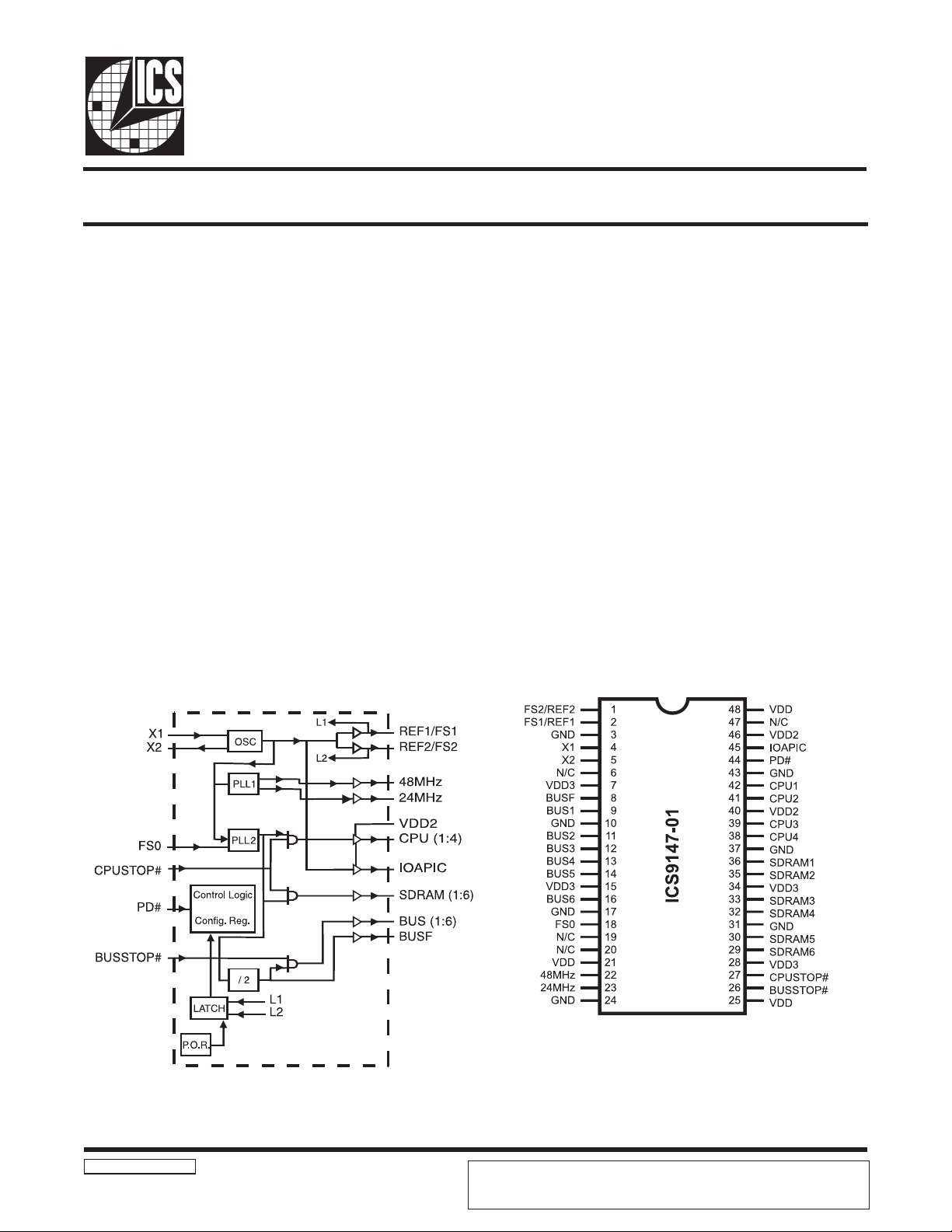
General Description Features
The ICS9147-01 generates all clocks required for high
speed RISC or CISC microprocessor systems such as Intel
PentiumPro. Two bidirectional I/O pins (FS1,FS2) are latched
at power-on to the functionality table, with FS0 selectable
in real-time to toggle between conditions. The inputs
provide for tristate and test mode conditions to aid in
system level testing. These multiplying factors can be
customized for specific applications. Glitch-free stop
clockcontrols are provided for CPU clocks and BUS clocks.
High drive BUS and SDRAM outputs typically provide
greater than 1 V/ns slew rate into 30pF loads. CPU outputs
typically provide better than 1V/ns slew rate into 20pF
loads while maintaining
outputs typically provide better than 0.5V/ns slew rates.
Seperate buffers supply pins VDD2 allow for 3.3V or
reduced voltage swing (from 2.9 to 2.5V) for CPU (1:4) and
IOAPIC outputs.
50 ±
5% duty cycle. The REF clock
• Four copies of CPU clock
• Six SDRAM (3.3 V TTL), usable as AGP clocks
• Seven copies of BUS clock (synchronous with CPU
clock/2 or CPU/2.5 for 75 and 83.3 MHz CPU)
• CPU clocks to BUS clocks skew 1-4ns (CPU early)
• One IOAPIC clock @14.31818 MHz
• Two copies of Ref. clock @14.31818 MHz
• One each 48/24 MHz (3.3 V TTL)
• This device is configured into the Mobile mode for
power management of Intel 430 TX
• Ref. 14.31818 MHz Xtal oscillator input
• Separate 66/60 MHz select pin (LSB of select pins)
• Separate V
buffers to allow 2.5V output (or Std. Vdd)
• Power Management Control Input pins
• 3.0V – 3.7V supply range w/2.5V compatible outputs
• 48-pin SSOP package
for four CPU and single IOAPIC output
DD2
TM
Block Diagram
Pin Configuration
48-Pin SSOP
9147-01Rev B 04/25/01
Pentium is a trademark of Intel Corporation
ICS reserves the right to make changes in the device data identified in this publication
without further notice. ICS advises its customers to obtain the latest version of all
device data to verify that any information being relied upon by the customer is current
and accurate.
Page 2
ICS9147-01
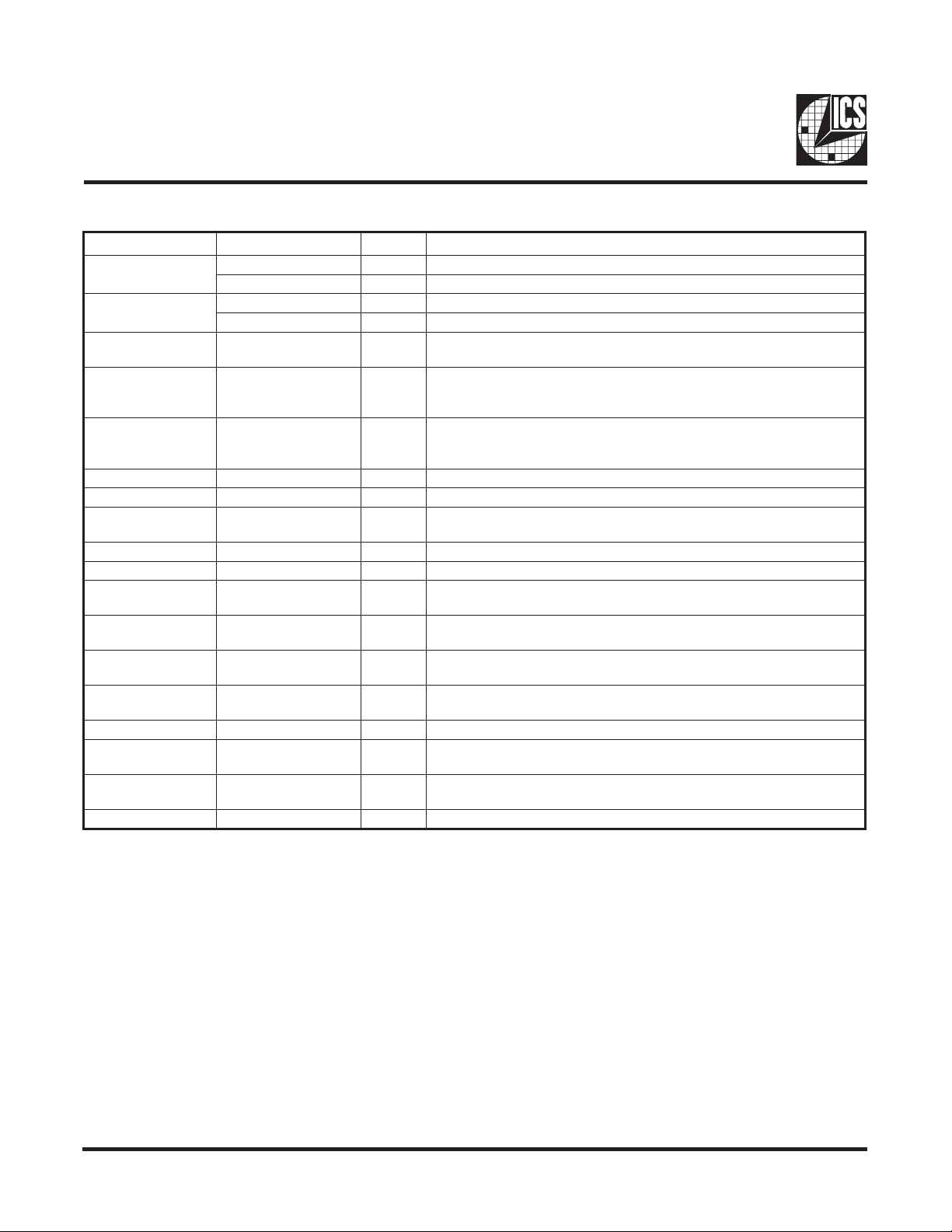
Pin Descriptions
REBMUNNIP EMANNIP EPYT NOITPIRCSED
1
2
,13,42,71,01,3
34,73
41XNI
52XTUO
43,82,51,73DDVRWP.ylppusreffubMARDSdnaSUB,ylppusrewopO/IV3.3
61,41,31,21,11,9,8)6:1(SUB,FSUBTUOycneuqerfrofelbattcelesees.stuptuokcolcSUB
81OSFNI
84,52,12DDVRWP.rewopkcolcdexifdna,ylppusrewoperoC
32,22zHM42,84TUOstuptuokcolczHM42,84
62#POTSSUBNI
72#POTSUPCNI
,03,23,33,53,63
92
64,042DDVRWP
83,93,24,14)4:1(UPCTUOycneuqerfrofelbattceleseeS.skcolctuptuokcolcUPC
44#DPNI
54CIPAOITUO
74,02,91,6C/N— .detcennocyllanretnitonsniP
2FERTUO*tuptuokcolcecnerefeR
2SFNI*2tiBtcelesycneuqerftupnicigoL
1FERTUO*tuptuokcolcecnerefeR
1SFNI*1tiBtcelesycneuqerftupnicigoL
DNGRWP.dnuorG
)6:1(MARDSTUO
lanretxE.pacdaollanretnisaH.zHM813.41yllanimoN.tupnilatsyrC
retsafnorewopDDVrofdednemmocerDNGotFp03fodaollatsyrc
.sm0.2naht
.1XotrotsiserkcabdeefdnapacdaollanretnisaH.tuptuolatsyrC
rewopDDVrofdednemmocerDNGotFp01fodaollatsyrclanretxE
.sm0.2nahtretsafno
nisnoitcelesrehtoro,zHM06rozHM6.66gnilbanerofniptceleS
.elbattcelesycneuqerf
sinipnehwskcolc)6:1(SUBllapotsylsuonorhcnysotniptupnI
.wol
nehwskcolcMARDSdnaUPCllapotsylsuonorhcnysotniptupnI
.wolsinip
.ycneuqerfrofelbattceleseeS.deepsUPCtaskcolcMARDS
.3DDVybderewoP
otdeitebnac,sreffubCIPAOIdnaUPCrofylppuSrewoPV5.2
noitarepoV3.3rof3DDV
LLPhtobffosrewop,wolnehW.tupnilortnoccigolnwodrewoP
.wolcigolotdecrofstuptuolladna
derewoP)latsyrclanimonhtiw813.41=qerF(tuptuokcolcCIPAOI
ylppus2DDVyb
* Bidirectional input/output pins, input logic levels are latched at internal power-on-reset. Use 10Kohm resistor to program logic
Hi to VDD or GND for logic low.
2
Page 3
ICS9147-01
1(UPC
Functionality
,)4:
#DP
11 1 0 0 0 06038442813.41
11 1 0 0 1 6.663.338442813.41
11 1 0 1 0 05528442813.41
11 1 0 1 1 555.728442813.41
11 1 1 0 0 5703
11 1 1 0 1 3.383.33
11 1 1 1 0 2/FER4/FER2/FER4/FERFER
11 1 1 1 1 etatsirTetatsirTetatsirTetatsirTetatsirT
01 1 X X X
10 1 X X X WOLgninnurgninnurgninnurgninnur
11 0 X X X gninnurWOLgninnurgninnurgninnur
Note a: These frequency selections are at CPU/2.5 (internal VCO/5), not synchronous CPU/2
-UPC
#POTS
-SUB
#POTS
*2SF
)2FERta(
*1SF
)1FERta(
0SF
)81nip(
MRDS
)6:1(
)zHM(
WOL
ffoLLP
)6:1(SUB
FSUB
)zHM(
a
a
WOL
zHM84
)zHM(
8442813.41
8442813.41
WOL
ffoLLP
zHM42
)zHM(
WOL
,)2:1(FER
CIPAOI
)zHM(
WOL
ffOcsO
3
Page 4
ICS9147-01
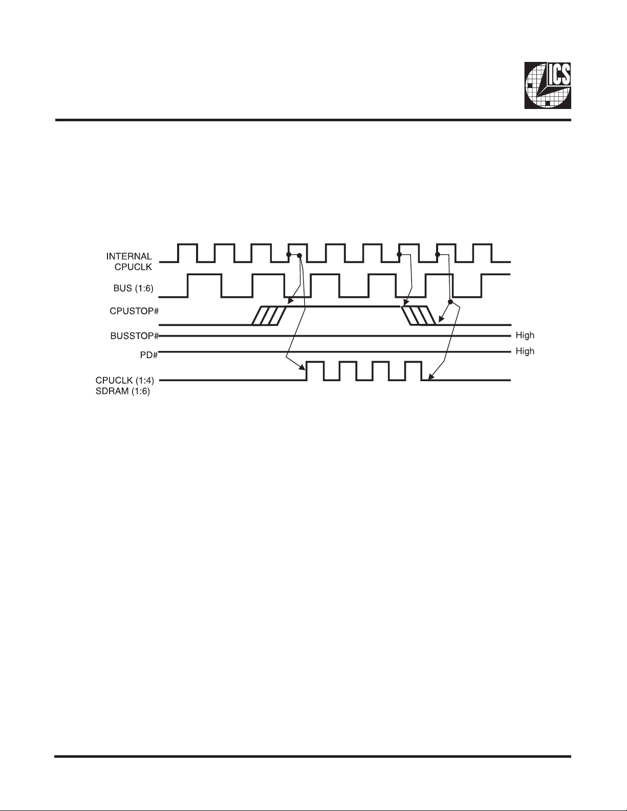
CPUSTOP# Timing Diagram
CPUSTOP# is an asychronous input to the clock synthesizer. It is used to turn off the CPU clocks for low power operation.
CPUSTOP# is synchronized by the ICS9147-01. All other clocks will continue to run while the CPU and SDRAM clocks
are disabled. The CPU and SDRAM clocks will always be stopped in a low state and start in such a manner that guarantees
the high pulse width is a full pulse. CPU clock on latency is 0 to 1 CPU clocks and CPU clock off latency is 0 to 1 CPU
clocks.
Notes:
1. All timing is referenced to the internal CPU clock.
2. CPUSTOP# is an asynchronous input and metastable conditions
may exist. This signal is synchronized to the CPU and SDRAM
clocks inside the ICS9147-01.
3. All other clocks continue to run undisturbed.
4. PD# and BUSSTOP# are shown in a high (true) state.
BUSSTOP# Timing Diagram
BUSSTOP# is an asynchronous input to the ICS9147-01. It is used to turn off the BUS (1:6) clocks for low power operation.
BUSSTOP# is synchronized by the ICS9147-01 internally. BUS (1:6) clocks are stopped in a low state and started with
a full high pulse width guaranteed. BUS (1:6) clock on latency cycles are less than 4 CPU clocks and BUS (1:6) clock off
latency is less than 4 clocks.
(Drawing shown on next page.)
4
Page 5

Notes:
1. All timing is referenced to the Internal BUS clock (defined as inside the ICS9147 device.)
2. BUSSTOP# is an asynchronous input, and metastable conditions may exist. This signal is required to be
synchronized inside the ICS9147.
3. All other clocks continue to run undisturbed.
4. PD# and CPUSTOP# are shown in a high (true) state.
ICS9147-01
PD# Timing Diagram
The power down selection is used to put the part into a very low power state without turning off the power to the part.
PD# is an asynchronous active low input. This signal is synchronized internal by the ICS9147-01 prior to its control
action of powering down the clock synthesizer. PD# is an asynchronous function for powering up the system. Internal
clocks will not be running after the device is put in power down state. When PD# is active (low) all clocks are driven to
a low state and held prior to turning off the VCOs and the Crystal oscillator. The power on latency is guaranteed to be
less than 3mS. The power down latency is less than three CPU clock cycles. BUSSTOP# and CPUSTOP# are don’t care
signals during the power down operations.
Notes:
1. All timing is referenced to the Internal CPU clock (defined as inside the ICS9147 device).
2. PD# is an asynchronous input and metastable conditions may exist. This signal is synchronized inside the ICS9147.
3. The shaded sections on the VCO and the Crystal signals indicate an active clock is being generated.
5
Page 6

ICS9147-01
Absolute Maximum Ratings
Supply Voltage. . . . . . . . . . . . . . . . . . . . . . . . . . 7.0 V
Logic Inputs . . . . . . . . . . . . . . . . . . . . . . . . . . . . GND –0.5 V to V
Ambient Operating Temperature . . . . . . . . . . 0°C to +70°C
Storage Temperature. . . . . . . . . . . . . . . . . . . . . –65°C to +150°C
Stresses above those listed under Absolute Maximum Ratings may cause permanent damage to the device. These ratings
are stress specifications only and functional operation of the device at these or any other conditions above those listed
in the operational sections of the specifications is not implied. Exposure to absolute maximum rating conditions for
extended periods may affect product reliability.
Electrical Characteristics at 3.3V
VDD = 3.0 – 3.7 V, TA = 0 – 70°C unless otherwise stated
RETEMARAPLOBMYSSNOITIDNOCTSETNIMPYTXAMSTINU
egatloVwoLtupnIVLIstupniemitlluFdnastupnidehctaL--V2.0DDV
egatloVhgiHtupnIVHIstupniemitlluFdnastupnidehctaLV7.0DD- - V
tnerruCwoLtupnIILIVNI)stupniemitlluF(V0=0.82-5.01--A
tnerruChgiHtupnIIHIVNIV=DD)stupniemitlluF(0.5--0.5A
tnerruCwoLtuptuO
tnerruChgiHtuptuO
tnerruCwoLtuptuOI2LOVLOFER,SUB,84,42dexifrof;V8.0=0.610.52-Am
tnerruChgiHtuptuOI2HOVHOFER,SUB,84,42dexifrof;V0.2=-0.22-0.41-Am
tnerruCwoLtuptuO
tnerruChgiHtuptuO
egatloVwoLtuptuO
egatloVhgiHtuptuO
egatloVwoLtuptuOV2LOILOsKLCdexifrof;Am8=-3.04.0V
egatloVhgiHtuptuOV2HOIHOsKLCdexifrof;Am8-=4.28.2-V
egatloVwoLtuptuO
egatloVhgiHtuptuO
tnerruCylppuSIDDdedaolnustuptuolla;zHM6.66@-021081Am
tnerruCylppuSIDPDDnwoDrewoP003005A
Ia1LOVLOV;MARDS,UPC;V8.0=2DDV3.3=0.910.03-Am
Ib1LOVLOV5.2=2DDV;UPC;V8.0=0.910.03Am
Ia1HOVHOV;MARDS,UPC;V0.2=2DDV3.3=-0.62-0.61-Am
Ib1HOVHOV;UPC;V0.2=2DDV5.2=5.21-5.9-Am
Ia3LOVLOV;CIPAOI;V8.0=2DDV3.3=0.910.33-Am
Ib3LOVLOV;CIPAOI;V8.0=2DDV5.2=0.910.33Am
Ia3HOVHOVtaCIPAOIrofV0.2=2DDV3.3=-0.54-0.61-Am
Ib3HOVHOV;CIPAOI;V0.2=2DDV5.2=0.31-0.01-Am
Va1LOILOV;MARDS,UPC;Am01=2DDV3.3=-3.04.0V
Vb1LOILOV;UPC;Am01=2DDV5.2=3.04.0V
Va1HOIHOV;MARDS,UPC;Am01-=DDV3.3=4.28.2-V
Vb1HOIHOV5.2=2DDV;UPC;Am01-=59.11.2V
Va3LOILOVtaCIPAOIrof;Am01=2DDV3.3=-3.04.0V
Vb3LOILOV5.2=2DDV;CIPAOI;Am01=3.04.0V
Va3HOIHOVtaCIPAOIrof;Am01-=2DDV3.3=4.28.2-V
Vb3HOIHOV;CIPAOI;Am01-=2DDV5.2=0.22.2-V
+0.5 V
DD
scitsiretcarahCCD
Note 1: Parameter is guaranteed by design and characterization. Not 100% tested in production.
6
Page 7

Electrical Characteristics at 3.3V
VDD = 3.0 – 3.7 V, TA = 0 – 70°C unless otherwise stated
scitsiretcarahCCA
RETEMARAPLOBMYSSNOITIDNOCTSETNIMPYTXAMSTINU
1
emiTesiR
1
emiTesiR
3,1
emiTllaF
1
emiTesiR
1
emiTllaF
1
emiTesiR
1
emiTllaF
3,1
emiTesiR
1
emiTesiR
3,1
emiTllaF
1
emiTesiR
1
emiTllaF
1
elcyCytuD
wekSkcolC
wekSkcolC
wekSkcolC
wekSkcolC
1
elcyCotelcyC,rettiJ
,12
amgiSenO,rettiJ
,12
etulosbA,rettiJ
1
amgiSenO,rettiJ
1
etulosbA,rettiJ
1
ycneuqerFtupnI
1
emiTno-rewoP
1
1
,12
1
1
ecnaticapaCtupnIcigoL
1
ecnaticapaCrotallicsOlatsyrC
Ta1r
Tb1r
T1f;UPCV8.0ot0.2,daolFp02-8.04.1sn
T2rV0.2ot8.0MARDSdaolFp03-0.16.1sn
T2fV8.0ot0.2MARDSdaolFp03-9.05.1sn
T3rV0.2ot8.0SUBdaolFp03-2.10.2sn
T3fV8.0ot0.2SUBdaolFp03-1.19.1sn
T4r
Ta4r
V5.2=LDDV
T4f
T5r
T5f
V3.3=DDV
V3.3=DDV
Dt V4.1=TUOV@daolFp02540555%
Tc-cjV7.3ot0.3=2DDV,UPC051052sp
T1s1j
T1baj
T2s1j
T2baj
C1FERLFp74=
C1FERLFp74=
Fi 0.21813.410.61zHM
CNIsniptupnicigoL-5-Fp
CXNIsnip2X,1X-81-Fp
tno
T1ks
)DDVemaS(
T2ksV4.1@;Fp02=daoL;SUBotSUB-003005sp
T3ks
T4ks
Note 1: Parameter is guaranteed by design and characterization. Not 100% tested in production.
Note 2: Includes VDD2 = 2.5V
Note 3: VDD3 = 3.3V
V0.2ot8.0,daolFp02
V3.3=DDV;UPC
V0.2ot8.0,daolFp02
V5.2@LDDV;UPC
V0.2ot8.0,daolFp02
CIPAOI&,2FER,84,42
htiwCIPAOI,V0.2ot8.0,daolFp54
V8.0ot0.2,daolFp02
CIPAOI&,2FER,84,42
-9.05.1sn
-5.10.2sn
-38.04.1sn
-2.26.2sn
-18.03.1sn
CIPAOIV0.2ot8.0Fp54=daoL
1FER,V8.0ot0.2Fp54=daoL
,Fp02=daoL;UPC
Fp03=daoLskcolCSUB&MARDS
-05051sp
,Fp02=daoL;UPC
p03=daoLskcolCSUB&MARDS
,Fp02=daoLzHM42/84,2FER
,Fp02=daoLzHM42/84,2FER
6.66fognissorcts1otV6.1=DDVmorF
sm04<pmarylppusDDVzHM
V4.1@;Fp02=daoL;UPCotUPC
V4.1@;Fp02=daoL;SUBotUPC
)ylraesiUPC(
-13%
5-25%
-5.25.4sm
-051052sp
16.24sn
)V5.2@(UPCot)V3.3@(MARDS
)etalsiUPCV5.2(
ICS9147-01
6.10.2sn
6.10.2sn
052--052sp
052004sp
7
Page 8

ICS9147-01
Shared Pin Operation Input/Output Pins
Pins 1 and 2 on the ICS9147-01 serve as dual signal functions
to the device. During initial power-up, they act as input
pins. The logic level (voltage) that is present on these pins at
this time is read and stored into a 4-bit internal data latch. At
the end of Power-On reset, (see AC characteristics for timing
values), the device changes the mode of operations for these
pins to an output function. In this mode the pins produce the
specified buffered clocks to external loads.
To program (load) the internal configuration register for
these pins, a resistor is connected to either the VDD (logic 1)
power supply or the GND (logic 0) voltage potential. A 10
Kilohm(10K) resistor is used to provide both the solid CMOS
programming voltage needed during the power-up
programming period and to provide an insignificant load on
the output clock during the subsequent operating period.
Figs. 1 and 2 show the recommended means of implementing
this function. In Fig. 1 either one of the resistors is loaded
onto the board (selective stuffing) to configure the device’s
internal logic. Figs. 2a and b provide a single resistor
loading option where either solder spot tabs or a physical
jumper header may be used.
These figures illustrate the optimal PCB physical layout
options. These configuration resistors are of such a large
ohmic value that they do not effect the low impedance clock
signals. The layouts have been optimized to provide as little
impedance transition to the clock signal as possible, as it
passes through the programming resistor pad(s).
Test Mode Operation
The ICS9147-01 includes a production test verification
mode of operation. This requires that the FSO and FS1 pins
be programmed to a logic high and the FS2 pin be
programmed to a logic low(see Shared Pin Operation
section). In this mode the device will output the following
frequencies.
niP ycneuqerF
CIPAOI,FERFER
zHM842/FER
zHM424/FER
,UPC
MARDS
)6:1(SUB4/FER
Note: REF is the frequency of either the crystal connected
between the devices X1and X2 or, in the case of a device
being driven by an external reference clock, the frequency
of the reference (or test) clock on the device’s X1 pin.
2/FER
Fig. 1
8
Page 9

ICS9147-01
Fig. 2a
Fig. 2b
9
Page 10

ICS9147-01
Recommended PCB Layout for ICS9147-01
NOTE:
This PCB Layout is based on a 4 layer board with an internal Ground (common) and Vcc plane. Placement of
components will depend on routing of signal trace. The 0.1uf Capacitors should be placed as close as possible
to the Power pins. Placement on the backside of the board is also possible. The Ferrite Beads can be replaced
with 10-15ohm Resistors. For best results, use a Fixed Voltage Regulator between the main (board) Vcc and the
different Vdd planes.
10
Page 11

ICS9147-01
INDEX
AREA
1 2
h x 45°
SEATING
PLANE
- C -
.10 (.004) C
MIN
MAX
MIN
MAX
A
2.41
2.80.095.110
A1
0.20
0.40.008.016b0.20
0.34.008.0135
0.13
0.25.005.010DE
10.03
10.68
420E17.40
7.60.291.299eh
0.38
0.64.015.025L0.50
1.02.020.040
Nα0°8°0°8°MIN
MAX
MIN
MAX4815.75
16.00
620.630
N
INDEX
AREA
12
D
e
b
300 mil SSOP Package
c
In Millimeters In Inches
L
E1
E
SYMBOL
COMMON DIMENSIONS COMMON DIMENSIONS
c
SEE VARIATIONS SEE VARIATIONS
.395.
h x 45°
a
0.635 BASIC 0.025 BASIC
A
A1
-C-
SEATING
PLANE
.10 (.004) C
N
Reference Doc.: JEDEC Publication 95, MO-118
10-0034
SEE VARIATIONS SEE VARIATIONS
VARIATIONS
D mm. D (inch)
.
Ordering Information
ICS9147F-01
Example:
ICS XXXX F - PPP
Pattern Number (2 or 3 digit number for parts with ROM code patterns)
Package Type
F=SSOP
Device Type (consists of 3 or 4 digit numbers)
Prefix
ICS = Standard Device
11
 Loading...